

Datasheet SN751730DR, SN751730N, SN751730NS, SN751730NSR, SN751730D Datasheet (Texas Instruments)
SN751730
TRIPLE LINE DRIVER/RECEIVER
SLLS062C – MAY 1990 – REVISED MAY 1995
1
POST OFFICE BOX 655303 • DALLAS, TEXAS 75265
D
Meets or Exceeds the Requirements of
IBM 360/370 Input/Output Interface
Specification for 4.5 Mb/s Operation
D
Single 5-V Supply
D
Uncommited Emmitter-Follower Output
Structure for Party-Line Operation
D
Driver Output Short-Circuit Protection
D
Driver Input/Receiver Output Compatible
With TTL
D
Receiver Input Resistance...7.4 kΩ
to 20 kΩ
D
Ratio Specification for Propagation Delay
Time, Low-to-High/High-to-Low
description
The SN751730 triple line driver/receiver is specifically designed to meet the input/output interface specifications
for IBM System 360/370. It is also compatible with standard TTL logic and supply voltage levels.
The low-impedance emitter-follower driver outputs of the SN751730 drive terminated lines such as coaxial
cable or twisted pair. Having the outputs uncommitted allows wired-OR logic to be performed in party-line
applications. Output short-circuit protection is provided by an internal clamping network that turns on when the
output voltage drops below approximately 2.5 V.
An open line affects the receiver input as does a low-level input voltage.
All the driver inputs and receiver outputs are in conventional TTL configuration and the gating can be used
during power-up and power-down sequences to ensure that no noise is introduced to the line by pulling either
DE1 or DE2 to a low level.
Function Tables
EACH DRIVER
INPUTS
OUTPUT
DI DE1 DE2
DO
L X X L
X LX L
XXL L
HHH H
EACH DRIVER
INPUT
RI
OUTPUT
RO
L H
H L
Open H
H = high level, L = low level,
X = irrelevant
Copyright 1995, Texas Instruments Incorporated
PRODUCTION DATA information is current as of publication date.
Products conform to specifications per the terms of Texas Instruments
standard warranty. Production processing does not necessarily include
testing of all parameters.
Please be aware that an important notice concerning availability, standard warranty, and use in critical applications of
Texas Instruments semiconductor products and disclaimers thereto appears at the end of this data sheet.
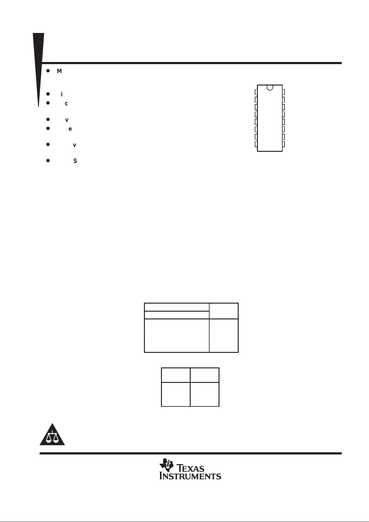
1
2
3
4
5
6
7
8
16
15
14
13
12
11
10
9
DE1
RI1
RO1
RI2
RO2
RI3
RO3
GND
V
CC
DO1
DI1
DO2
DI2
DO3
DI3
DE2
(TOP VIEW)
D OR N PACKAGE
IBM is a trademark of International Business Machines Corporation.
SN751730
TRIPLE LINE DRIVER/RECEIVER
SLLS062C – MAY 1990 – REVISED MAY 1995
2
POST OFFICE BOX 655303 • DALLAS, TEXAS 75265
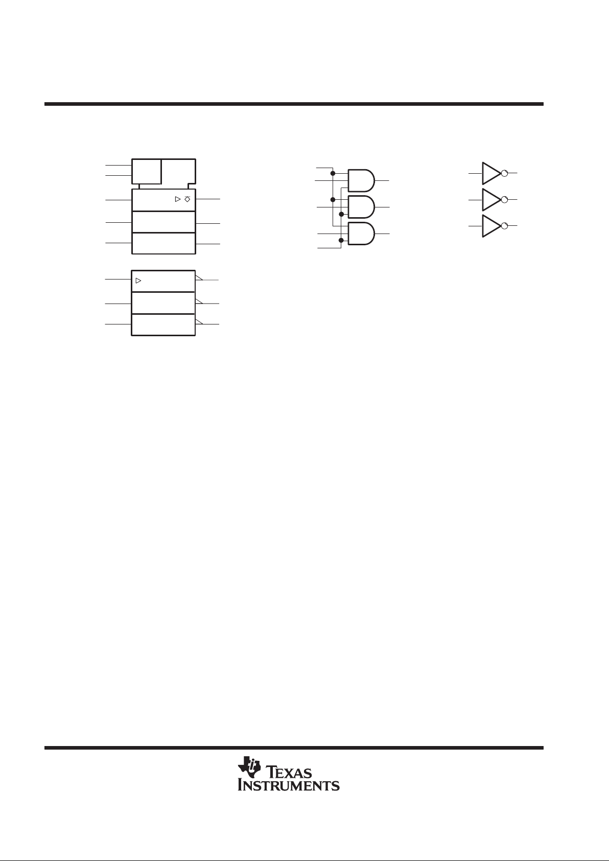
logic symbols
†
&
EN
DE1
DE2
DI1
DI2
DI3
2
RI1
4
RI2
6
RI3
DO1
15
DO2
13
DO3
11
RO1
RO2
DRIVER
RECEIVER
RO3
3
5
7
†
These symbols are in accordance with ANSI/IEE Std 91-1984
and IEC Publication 617-12.
1
12
9
14
10
logic diagrams (positive logic)
DO1
15
DO2
13
DO3
11
DE1
DI1
DI2
DI3
DE2
DRIVER
1
14
12
10
9
2
RI1
RO1
3
4
RI2
RO2
5
6
RI3
RO3
7
RECEIVER
SN751730
TRIPLE LINE DRIVER/RECEIVER
SLLS062C – MAY 1990 – REVISED MAY 1995
3
POST OFFICE BOX 655303 • DALLAS, TEXAS 75265
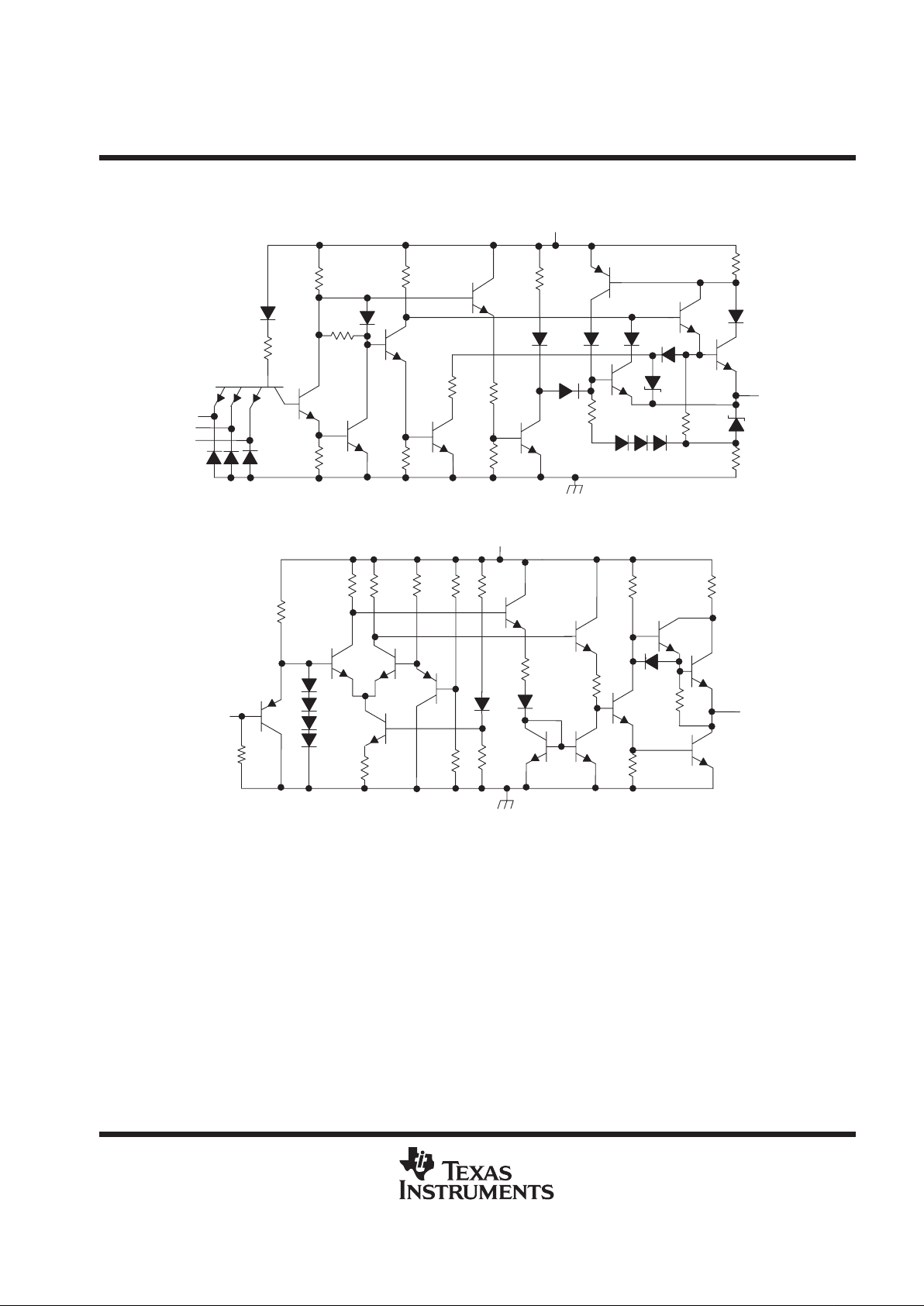
equivalent schematics of driver and receiver
†
DRIVER
RECEIVER
V
CC
V
CC
15 kΩ
2.5 Ω
DO
100 Ω
6 kΩ
60 Ω
RI
14 kΩ
RO
DI
DE1
DE2
†
All resistor values are nominal.

SN751730
TRIPLE LINE DRIVER/RECEIVER
SLLS062C – MAY 1990 – REVISED MAY 1995
4
POST OFFICE BOX 655303 • DALLAS, TEXAS 75265
absolute maximum ratings over operating free-air temperature range (unless otherwise noted)
†
Supply voltage, V
CC
(see Note 1) 7 V. . . . . . . . . . . . . . . . . . . . . . . . . . . . . . . . . . . . . . . . . . . . . . . . . . . . . . . . . . . . .
Input voltage range, V
I
: Driver –0.5 V to 7 V. . . . . . . . . . . . . . . . . . . . . . . . . . . . . . . . . . . . . . . . . . . . . . . . . . . . . . .
Receiver –0.5 V to 7 V. . . . . . . . . . . . . . . . . . . . . . . . . . . . . . . . . . . . . . . . . . . . . . . . . . . . .
Output voltage range, V
O
: Driver –0.5 V to 7 V. . . . . . . . . . . . . . . . . . . . . . . . . . . . . . . . . . . . . . . . . . . . . . . . . . . . .
Enable input voltage range –0.5 V to 7 V. . . . . . . . . . . . . . . . . . . . . . . . . . . . . . . . . . . . . . . . . . . . . . . . . . . . . . . . . .
Continuous total power dissipation See Dissipation Rating Table. . . . . . . . . . . . . . . . . . . . . . . . . . . . . . . . . . . . .
Operating free-air temperature range, T
A
0°C to 70°C. . . . . . . . . . . . . . . . . . . . . . . . . . . . . . . . . . . . . . . . . . . . . .
Storage temperature range, T
stg
–65°C to 150°C. . . . . . . . . . . . . . . . . . . . . . . . . . . . . . . . . . . . . . . . . . . . . . . . . . .
Lead temperature 1,6 mm (1/16 inch) from case for 10 seconds 260°C. . . . . . . . . . . . . . . . . . . . . . . . . . . . . . .
†
Stresses beyond those listed under “absolute maximum ratings” may cause permanent damage to the device. These are stress ratings only, and
functional operation of the device at these or any other conditions beyond those indicated under “recommended operating conditions” is not
implied. Exposure to absolute-maximum-rated conditions for extended periods may affect device reliability.
NOTE 1: All voltage values are with respect to network ground terminal.
DISSIPATION RATING TABLE
TA ≤ 25°C DERATING FACTOR TA = 70°C
PACKAGE
A
POWER RATING ABOVE TA = 25°C
A
POWER RATING
D 950 mV 7.6 mW/°C 608 mW
N 1150 mV 9.2 mW/°C 736 mW
recommended operating conditions
MIN NOM MAX UNIT
Supply voltage, V
CC
4.75 5 5.25 V
p
Driver, Enable 2
High-level input voltage, V
IH
Receiver 1.55
V
p
Driver, Enable 0.8
Low-level input voltage, V
IL
Receiver 1.15
V
Operating free-air temperature, T
A
0 70 °C

SN751730
TRIPLE LINE DRIVER/RECEIVER
SLLS062C – MAY 1990 – REVISED MAY 1995
5
POST OFFICE BOX 655303 • DALLAS, TEXAS 75265
DRIVER SECTION
electrical characteristics over recommended ranges of supply voltage and operating free-air
temperature (unless otherwise noted)
PARAMETER TEST CONDITIONS MIN MAX UNIT
V
IK
Input clamp voltage VCC = 4.75 V , IIL = –18 mA –1.5 V
V
= 4.75 V , V
= 2 V,
CC
,
IOH = –59.3 mA
IH
,
TA = 25°C
3.11
V
= 5.25 V ,
V
= 2 V
,
p
CC
,
IOH = –78.1 mA
V
IH
2
V,
4.10
VOHHigh-level output voltage
V
= 4.75 V ,
V
= 2 V
,
V
CC
,
RL = 51.4 Ω
V
IH
2
V,
3.05
V
= 5.25 V ,
V
= 2 V
,
CC
,
RL = 56.9 Ω
V
IH
2
V,
4.20
V
ODH
Differential high-level output voltage RL = 46.3 Ω or 56.9 Ω 0.50 V
V
CC
= 5.25 V,
I
OL
= –
0.24 mA
0.15
VOLL
ow-level output voltage
V
IL
= 0.8 V,
VIH = 4.5 V
RL = 56.9 Ω 0.15
V
p
DI
20
IIHHigh-level input current
DE
V
CC
= 5.25 V,
V
IH
= 2.7
V
60
µ
A
p
DI
–400
IILLow-level input current
DE
V
CC
= 5.25 V,
V
IH
= 0.4
V
–1200
µ
A
p
V
= 4.75 V ,
VIL = 0 100
IOHHigh-level output current
CC
,
VOH = 5 V
VIH = 4.5 V 100
µ
A
I
OS
Short-circuit output current
†
VCC = 5.25 V VIH = 4.5 V –30 mA
V
= 4.5 V,
I
CCH
pp
p
VCC = 5.25 V ,
I(D)
,
V
I(R)
= 0
47
Supply current (total package)
CC
No load
V
I
(D)
= 0,
mA
I
CCL
I(D)
V
I(R)
= 4.5 V
80
†
No more than one output should be shorted at a time, and duration of the short circuit should not exceed one second.
switching characteristics, VCC = 5 V ±5%, T
A
= 25°C
PARAMETER TEST CONDITIONS MIN TYP MAX UNIT
t
PLH
Propagation delay time, low- to high-level output 6.5 12 18.5 ns
t
PHL
Propagation delay time, high- to low-level output
RL = 47.5 Ω, See Figure 1
6.5 12 18.5 ns
∆t
pd
Differential propagation delay time
‡
10 ns
t
r
Output rise time
VCC = 5 V,
VO = 0.15 V to 3.05 V ,
p
5 10 ns
t
f
Output fall time
R
L
= 47.5 Ω,
See Figure 1
C
L
= 10.2 pF,
5
13 ns
VO = 1 V to 3 V average,
p
SR
Slew rate
R
L
= 47.5 Ω,
C
L
= 10.2 F,
See Figure 1
0.65
V/ns
‡
∆tpd = |t
PLH
– t
PHL
|

SN751730
TRIPLE LINE DRIVER/RECEIVER
SLLS062C – MAY 1990 – REVISED MAY 1995
6
POST OFFICE BOX 655303 • DALLAS, TEXAS 75265
RECEIVER SECTION
electrical characteristics over recommended ranges of supply voltage and operating free-air
temperature (unless otherwise noted)
PARAMETER TEST CONDITIONS MIN MAX UNIT
p
V
= 4.75 V , V
= 1.15 V ,
VOHHigh-level output voltage
CC
,
IOH = –400 µA
I
,
2.7
V
p
VCC = 4.75 V ,
I
OL
= 8
mA
0.5
VOLLow-level output voltage
CC
VIH = 1.55 V
IOL = 4 mA 0.4
V
r
I
Input resistance VCC = 0, VI = 0.15 V to 3.9 V 7.4 20 kΩ
I
IH
High-level input current VCC = 4.75 V , VIH = 3.11 V 0.42 mA
I
IL
Low-level input current VCC = 5.25 V , VIL = 0.15 V –0.24 0.04 mA
I
OS
†
Short-circuit output current VCC = 5.25 V , VIL = 0 –20 –100 mA
V
= 4.5 V,
I
CCH
pp
p
VCC = 5.25 V ,
I(D)
,
V
I(R)
= 0
47
Supply current (total package)
CC
No load
V
I
(D)
= 0,
mA
I
CCL
I(D)
V
I(R)
= 4.5 V
80
†
Only one output should be shorted at a time, and duration of the short circuit should not exceed one second.
switching characteristics, VCC = 5 V ±5%, T
A
= 25°C
PARAMETER TEST CONDITIONS MIN TYP MAX UNIT
t
PLH
Propagation delay time, low- to high-level output 7.5 12 19.5 ns
t
PHL
Propagation delay time, high- to low-level output
RL = 2 kΩ, CL = 15 pF, See Figure 2
7.5 12 19.5 ns
∆t
pd
‡
Differential propagation delay time 10 ns
‡
∆tpd = |t
PLH
– t
PHL
|

SN751730
TRIPLE LINE DRIVER/RECEIVER
SLLS062C – MAY 1990 – REVISED MAY 1995
7
POST OFFICE BOX 655303 • DALLAS, TEXAS 75265
PARAMETER MEASUREMENT INFORMATION
3 V
0 V
Input
Output
V
OH
V
OL
Input
Output
1.3 V
1.3 V
3.05 V
1.4 V
0.15 V
1.4 V
VCC = 5 V
TEST CIRCUIT VOLTAGE WAVEFORMS
50 Ω
C
L
(see Note B)
RL = 47.5 Ω
t
w
t
r
t
f
t
PHL
t
PLH
Pulse
Generator
(see Note A)
NOTES: A. The pulse generator has the following characteristics: ZO ≈ 50 Ω, tw ≤ 500 ns, PRR ≤ 1 MHz, tf ≤ 6 ns, tr ≤ 15 ns.
B. CL includes probe and jig capacitance.
Figure 1. Driver Test Circuit and Voltage Waveforms
Input
Output
3 V
0 V
V
OH
V
OL
Input
Output
1.3 V
1.3 V
1.4 V1.4 V
VOLTAGE WAVEFORMSTEST CIRCUIT
CL = 15 pF
(see Note B)
1N3064X2
RL = 2 kΩ
VCC = 5 V
t
w
t
PHL
t
PLH
Pulse
Generator
(see Note A)
NOTES: A. The pulse generator has the following characteristics: ZO ≈ 50 Ω, tw ≤ 500 ns, PRR ≤ 1 MHz, tf ≤ 10 ns, tr ≤ 10 ns.
B. CL includes probe and jig capacitance.
Figure 2. Receiver Test Circuit and Voltge Waveforms

IMPORTANT NOTICE
T exas Instruments and its subsidiaries (TI) reserve the right to make changes to their products or to discontinue
any product or service without notice, and advise customers to obtain the latest version of relevant information
to verify, before placing orders, that information being relied on is current and complete. All products are sold
subject to the terms and conditions of sale supplied at the time of order acknowledgement, including those
pertaining to warranty, patent infringement, and limitation of liability.
TI warrants performance of its semiconductor products to the specifications applicable at the time of sale in
accordance with TI’s standard warranty. T esting and other quality control techniques are utilized to the extent
TI deems necessary to support this warranty. Specific testing of all parameters of each device is not necessarily
performed, except those mandated by government requirements.
CERT AIN APPLICATIONS USING SEMICONDUCTOR PRODUCTS MAY INVOLVE POTENTIAL RISKS OF
DEATH, PERSONAL INJURY, OR SEVERE PROPERTY OR ENVIRONMENTAL DAMAGE (“CRITICAL
APPLICATIONS”). TI SEMICONDUCTOR PRODUCTS ARE NOT DESIGNED, AUTHORIZED, OR
WARRANTED TO BE SUITABLE FOR USE IN LIFE-SUPPORT DEVICES OR SYSTEMS OR OTHER
CRITICAL APPLICATIONS. INCLUSION OF TI PRODUCTS IN SUCH APPLICA TIONS IS UNDERST OOD TO
BE FULLY AT THE CUSTOMER’S RISK.
In order to minimize risks associated with the customer’s applications, adequate design and operating
safeguards must be provided by the customer to minimize inherent or procedural hazards.
TI assumes no liability for applications assistance or customer product design. TI does not warrant or represent
that any license, either express or implied, is granted under any patent right, copyright, mask work right, or other
intellectual property right of TI covering or relating to any combination, machine, or process in which such
semiconductor products or services might be or are used. TI’s publication of information regarding any third
party’s products or services does not constitute TI’s approval, warranty or endorsement thereof.
Copyright 1998, Texas Instruments Incorporated
 Loading...