

SN75159
DUAL DIFFERENTIAL LINE DRIVER
WITH 3-STATE OUTPUTS
SLLS088B – JANUARY 1977 – REVISED MA Y 1995
1
POST OFFICE BOX 655303 • DALLAS, TEXAS 75265
D
Meets or Exceeds the Requirements of
ANSI EIA/TIA-422-B and ITU
Recommendation V.11
D
Single 5-V Supply
D
Balanced Line Operation
D
TTL Compatible
D
High-Impedance Output State for
Party-Line Applications
D
High-Current Active-Pullup Outputs
D
Short-Circuit Protection
D
Dual Channels
D
Clamp Diodes at Inputs
description
The SN75159 dual differential line driver with 3-state outputs is designed to provide all the features of the
SN75158 line driver with the added feature of driver output controls. There is an individual control for each driver.
When the output control is low, the associated outputs are in a high-impedance state and the outputs can neither
drive nor load the bus. This permits many devices to be connected together on the same transmission line for
party-line applications.
The SN75159 is characterized for operation from 0°C to 70°C.
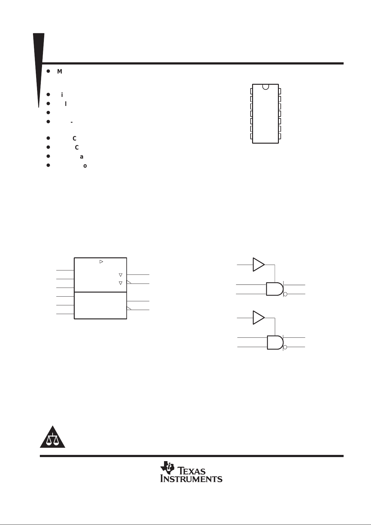
logic symbol
†
EN
1EN
1A
1B
2EN
2A
2B
&
1Z
3
2
12
13
6
4
5
9
10
11
1Y
2Y
2Z
†
This symbol is in accordance with ANSI/IEEE Std 91-1984
and IEC Publication 617-12.
logic diagram (positive logic)
6
4
5
9
10
11
3
2
12
13
1Y
1Z
2Y
2Z
1EN
1A
1B
2EN
2A
2B
Copyright 1995, Texas Instruments Incorporated
PRODUCTION DATA information is current as of publication date.
Products conform to specifications per the terms of Texas Instruments
standard warranty. Production processing does not necessarily include
testing of all parameters.
Please be aware that an important notice concerning availability, standard warranty, and use in critical applications of
Texas Instruments semiconductor products and disclaimers thereto appears at the end of this data sheet.
1
2
3
4
5
6
7
14
13
12
11
10
9
8
NC
1Z
1Y
1A
1B
1EN
GND
V
CC
2Z
2Y
2B
2A
2EN
NC
D OR N PACKAGE
(TOP VIEW)
NC–No internal connection
SN75159
DUAL DIFFERENTIAL LINE DRIVER
WITH 3-STATE OUTPUTS
SLLS088B – JANUARY 1977 – REVISED MA Y 1995
2
POST OFFICE BOX 655303 • DALLAS, TEXAS 75265
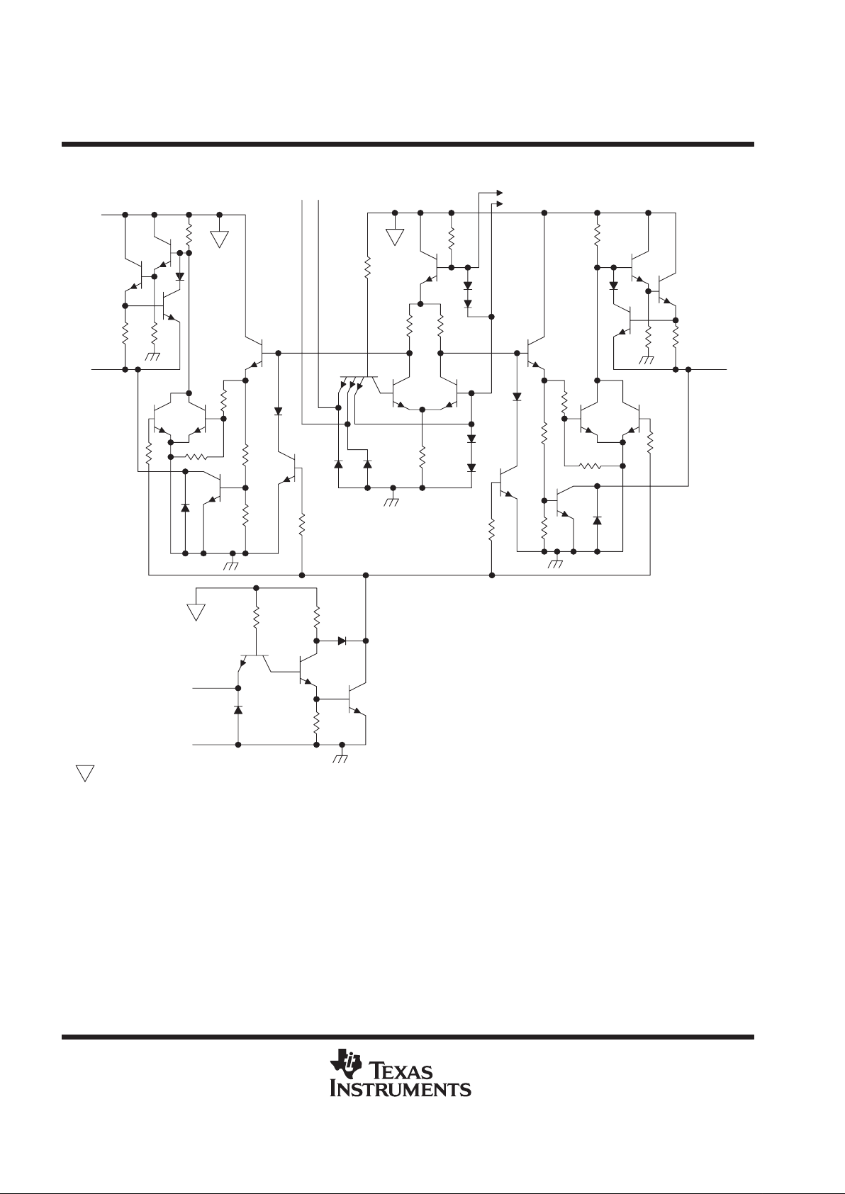
schematic (each driver)
5, 11
V
. . . VCC busV
Z
9 Ω
2, 13
Driver
To Other
4 kΩ
A
4, 10
B
V
CC
14
3, 12
9 Ω
V
GND
EN
7
6, 9
4 kΩ
V
Y
Resistor values shown are nominal.
SN75159
DUAL DIFFERENTIAL LINE DRIVER
WITH 3-STATE OUTPUTS
SLLS088B – JANUARY 1977 – REVISED MA Y 1995
3
POST OFFICE BOX 655303 • DALLAS, TEXAS 75265
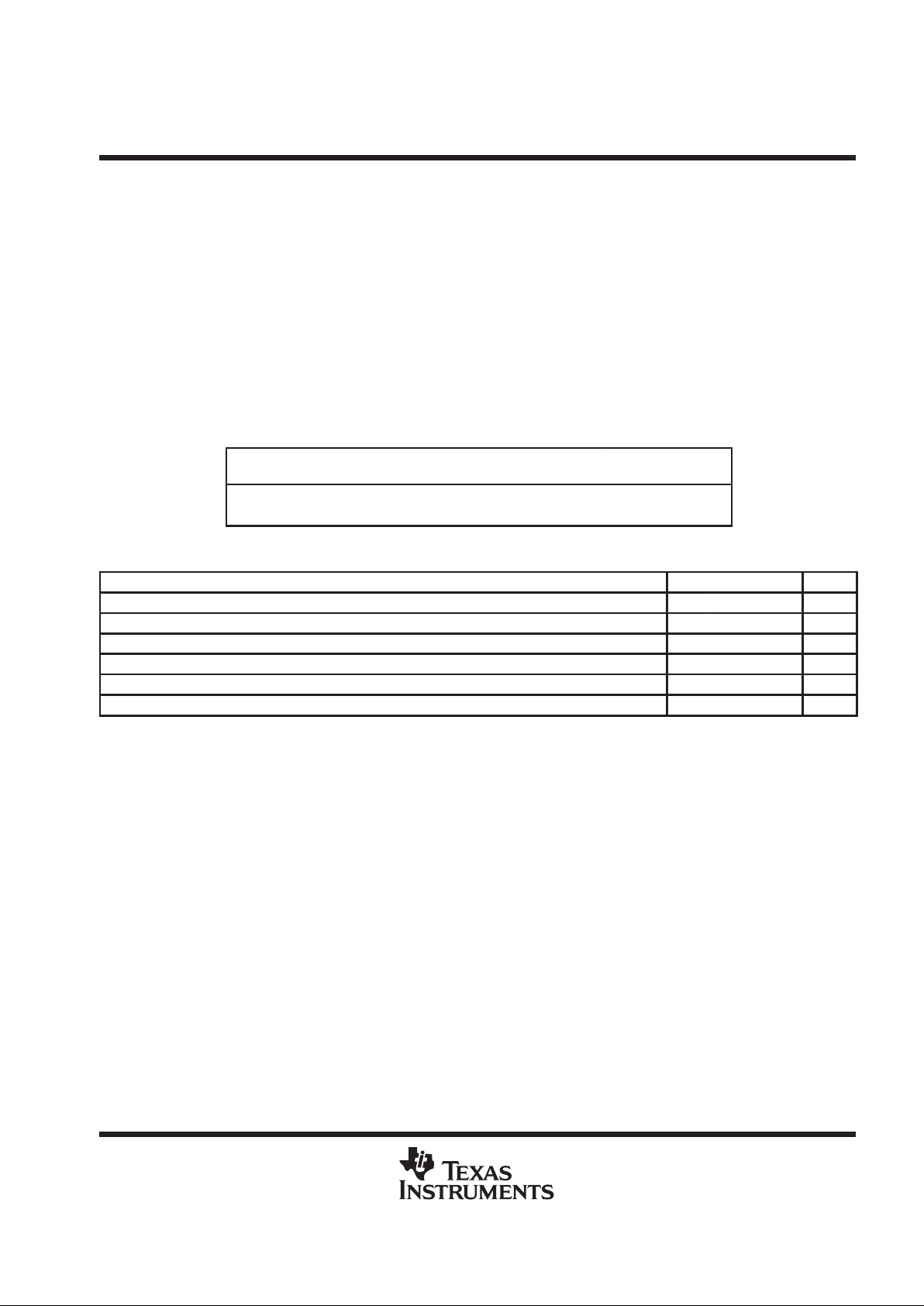
absolute maximum ratings over operating free-air temperature range (unless otherwise noted)
†
Supply voltage, V
CC
(see Note 1) 7 V. . . . . . . . . . . . . . . . . . . . . . . . . . . . . . . . . . . . . . . . . . . . . . . . . . . . . . . . . . . . .
Input voltage, V
I
5.5 V. . . . . . . . . . . . . . . . . . . . . . . . . . . . . . . . . . . . . . . . . . . . . . . . . . . . . . . . . . . . . . . . . . . . . . . . . .
Off-state voltage applied to open-collector outputs 12 V. . . . . . . . . . . . . . . . . . . . . . . . . . . . . . . . . . . . . . . . . . . . .
Continuous total dissipation See Dissipation Rating Table. . . . . . . . . . . . . . . . . . . . . . . . . . . . . . . . . . . . . . . . . . . .
Operating free-air temperature range, T
A
0°C to 70°C. . . . . . . . . . . . . . . . . . . . . . . . . . . . . . . . . . . . . . . . . . . . . .
Storage temperature range, T
stg
–65°C to 150°C. . . . . . . . . . . . . . . . . . . . . . . . . . . . . . . . . . . . . . . . . . . . . . . . . . .
Lead temperature 1,6 mm (1/16 inch) from case for 10 seconds 260°C. . . . . . . . . . . . . . . . . . . . . . . . . . . . . . .
†
Stresses beyond those listed under “absolute maximum ratings” may cause permanent damage to the device. These are stress ratings only, and
functional operation of the device at these or any other conditions beyond those indicated under “recommended operating conditions” is not
implied. Exposure to absolute-maximum-rated conditions for extended periods may affect device reliability.
NOTE 1: All voltage values except differential output voltage VOD are with respect to the network ground terminal. VOD is at the Y output with
respect to the Z output.
DISSIPATION RATING TABLE
PACKAGE
TA ≤ 25°C
POWER RATING
DERATING FACTOR
ABOVE TA = 25°C
TA = 70°C
POWER RATING
D 950 mW 7.6 mW/°C 608 mW
N 1150 mW 9.2 mW/°C 736 mW
recommended operating conditions
MIN NOM MAX UNIT
Supply voltage, V
CC
4.75 5 5.25 V
High-level input voltage, V
IH
2 V
Low-level input voltage, V
IL
0.8 V
High-level output voltage, I
OH
–40 mA
Low-level output current, I
OL
40 mA
Operating free-air temperature, T
A
0 70 °C
SN75159
DUAL DIFFERENTIAL LINE DRIVER
WITH 3-STATE OUTPUTS
SLLS088B – JANUARY 1977 – REVISED MA Y 1995
4
POST OFFICE BOX 655303 • DALLAS, TEXAS 75265
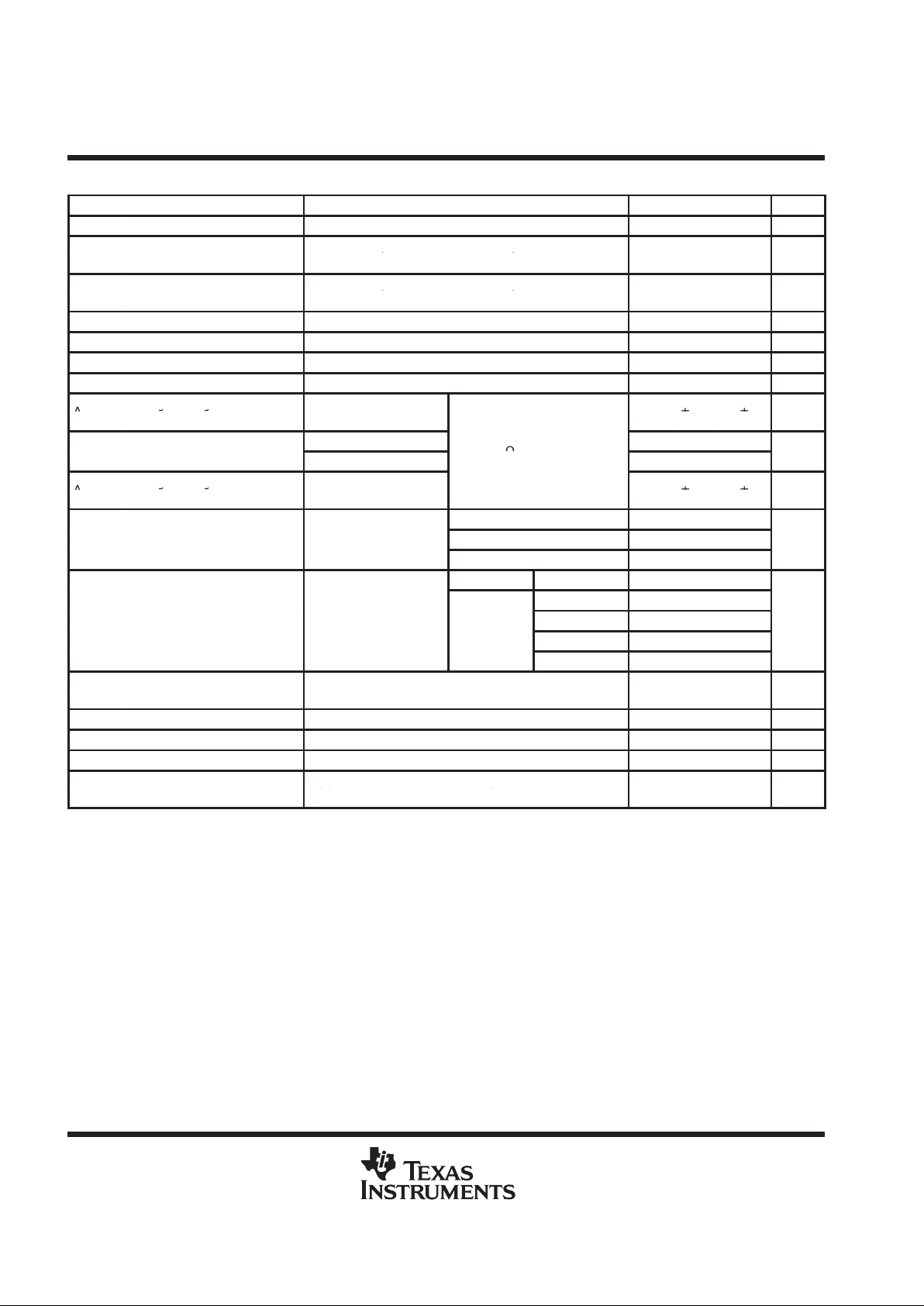
electrical characteristics over operating free-air temperature range (unless otherwise noted)
PARAMETER TEST CONDITIONS MIN TYP
†
MAX UNIT
V
IK
Input clamp voltage VCC = 4.75 V , II = –12 mA –0.9 –1.5 V
p
V
= 4.75 V , V
= 0.8 V,
VOHHigh-level output voltage
CC
,
VIH = 2 V,
IL
,
IOH = –40 mA
2.43V
p
V
= 4.75 V , V
= 0.8 V,
VOLLow-level output voltage
CC
,
VIH = 2 V,
IL
,
IOL = 40 mA
0.25
0.4
V
V
OK
Output clamp voltage VCC = 5.25 V , IO = –40 mA –1.1 –1.5 V
V
O
Output voltage VCC = 4.75 V to 5.25 V , IO = 0 0 6 V
|V
OD1
| Differential output voltage VCC = 5.25 V , IO = 0 3.5 2V
OD2
V
|V
OD2
| Differential output voltage VCC = 4.75 V 2 3 V
Change in magnitude of
∆|VOD|
gg
differential output voltage
‡
V
CC
= 4.75
V
±0.02
±0.4
V
Common-mode output
VCC = 5.25 V
1.8 3
V
OC
voltage
§
VCC = 4.75 V
R
L
=
100 Ω
,
See Figure 1
1.5 3
V
Change in magnitude of
∆|VOC|
gg
common-mode output voltage
‡
V
CC
= 4.75 V to 5.
25 V
±0.01
±0.4
V
VO = 6 V 0.1 100
I
O
Output current with power off VCC = 0
VO = –0.25 V –0.1 –100
µA
VO = –0.25 V to 6 V ±100
TA = 25°C VO = 0 to V
CC
±10
VO = 0 –20
I
OZ
Off-state (high-impedance
p
VCC = 5.25 V ,
p
°
VO = 0.4 V ±20
µA
state) out ut current
Out ut controls at 0.8V
T
A
=
70°C
VO = 2.4 V ±20
VO = V
CC
20
Input current at maximum input
I
I
voltage
V
CC
= 5.25 V,
V
I
= 5.5
V
1
mA
I
IH
High-level input current VCC = 5.25 V , VI = 2.4 V 40 µA
I
IL
Low-level input current VCC = 5.25 V , VI = 0.4 V –1 –1.6 mA
I
OS
Short-circuit output current
¶
VCC = 5.25 V –40 –90 –150 mA
pp
VCC = 5.25 V , Inputs grounded,
ICCSupply current (both drivers)
CC
TA = 25°C,
g
No load
4765mA
†
All typical values are at VCC = 5 V and TA = 25°C except for VOC, for which VCC is as stated under test conditions.
‡
∆|VOD| and ∆|VOC| are the changes in magnitudes of VOD and VOC, respectively, that occur when the input is changed from a high level to a low
level.
§
In ANSI Standard EIA/TIA-422-B, VOC, which is the average of the two output voltages with respect to GND, is called output offset voltage, VOS.
¶
Only one output should be shorted at a time, and duration of the short circuit should not exceed one second.

SN75159
DUAL DIFFERENTIAL LINE DRIVER
WITH 3-STATE OUTPUTS
SLLS088B – JANUARY 1977 – REVISED MA Y 1995
5
POST OFFICE BOX 655303 • DALLAS, TEXAS 75265
switching characteristics over operating free-air temperature range, VCC = 5 V
PARAMETER TEST CONDITIONS MIN TYP†MAX UNIT
t
PLH
Propagation delay time, low-to-high-level output
C
= 30 pF, R
= 100 Ω, See Figure 2,
16 25 ns
t
PHL
Propagation delay time, high-to-low-level output
L
,
L
,g,
Termination A
11 20 ns
t
PLH
Propagation delay time, low-to-high-level output
p
13 20 ns
t
PHL
Propagation delay time, high-to-low-level output
C
L
=
15 pF,See Figure 2,Termination B
9 15 ns
t
TLH
Transition time, low-to-high-level output
C
= 30 pF, R
= 100 Ω, See Figure 2,
4 20 ns
t
THL
Transition time, high-to-low-level output
L
,
L
,g,
Termination A
4 20 ns
t
PZH
Output enable time to high level CL = 30 pF, RL = 180 Ω, See Figure 3 7 20 ns
t
PZL
Output enable time to low level CL = 30 pF, RL = 250 Ω, See Figure 4 14 40 ns
t
PHZ
Output disable time from high level CL = 30 pF, RL = 180 Ω, See Figure 3 10 30 ns
t
PLZ
Output disable time from low level CL = 30 pF, RL = 250 Ω, See Figure 4 17 35 ns
Overshoot factor RL = 100 Ω, See Figure 2, Termination C 10%
†
All typical values are at TA = 25°C.
SYMBOL EQUIVALENTS
DATA-SHEET PARAMETER
EIA/TIA-422-B
V
O
V
oa, Vob
|V
OD1
| V
o
|V
OD2
| V
t
∆|VOD| ||Vt| – |Vt||
V
OC
|Vos|
∆|VOC| |Vos – Vos|
I
OS
|Isa| , |Isb|
I
O
|Ixa| , |Ixb|
PARAMETER MEASUREMENT INFORMATION
V
OC
50 Ω
50 Ω
V
OD2
Figure 1. Differential and Common-Mode Output Voltages

SN75159
DUAL DIFFERENTIAL LINE DRIVER
WITH 3-STATE OUTPUTS
SLLS088B – JANUARY 1977 – REVISED MA Y 1995
6
POST OFFICE BOX 655303 • DALLAS, TEXAS 75265
PARAMETER MEASUREMENT INFORMATION
100%
10%
VOLTAGE WAVEFORMS
t
PHL
t
PLH
90%90%
10% 10%
1.5 V1.5 V
90%
t
THL
t
TLH
10%
1.5 V
t
TLH
t
THL
10%
1.5 V
90%
Z Output
Y Output
V
OL
V
OH
V
OL
V
OH
0 V
t
PHL
t
PLH
1.5 V
90%
5 ns
Input
10%
1.5 V
90%
3 V
5 ns
25 ns
Overshoot
0%
TEST CIRCUITS
Z
Y
TERMINATION C
TERMINATION B
RL = 100 Ω
CL = 15 pF
(see Note B)
Z
Y
RL = 100 Ω
TERMINATION A
Z
Y
5 V
1 kΩ
Z Output
Y Output
50 Ω
Input
(see Note A)
Generator
Pulse
CL= 30 pF
(see Note B)
NOTES: A. The pulse generator has the following characteristics: ZO = 50 Ω, PRR ≤ 10 MHz.
B. CL includes probe and jig capacitance.
CL= 15 pF
(see Note B)
Overshoot
Figure 2. Test Circuits, Voltage Waveforms, and Overshoot Factor

SN75159
DUAL DIFFERENTIAL LINE DRIVER
WITH 3-STATE OUTPUTS
SLLS088B – JANUARY 1977 – REVISED MA Y 1995
7
POST OFFICE BOX 655303 • DALLAS, TEXAS 75265
PARAMETER MEASUREMENT INFORMATION
10%
VOLTAGE WAVEFORMS
TEST CIRCUIT
Output
RL = 180 Ω
5 V
1 kΩ
Input
50 Ω
(see Note A)
Generator
Pulse
0.5 V
V
off
= 0
V
OH
0 V
1.5 V
t
PHZ
Output
≤5 ns
t
PZH
1.5 V
90%
Input
3 V
10%
100 ns
1.5 V
90%
CL = 30 pF
(see Note B)
CL= 30 pF
(see Note B)
NOTES: A. The pulse generator has the following characteristics: ZO = 50 Ω, PRR ≤ 500 kHz.
B. CL includes probe and jig capacitance.
≤5 ns
Figure 3. Test Circuit and Voltage Waveforms

SN75159
DUAL DIFFERENTIAL LINE DRIVER
WITH 3-STATE OUTPUTS
SLLS088B – JANUARY 1977 – REVISED MA Y 1995
8
POST OFFICE BOX 655303 • DALLAS, TEXAS 75265
PARAMETER MEASUREMENT INFORMATION
5 V
VOLTAGE WAVEFORMS
TEST CIRCUIT
V
OL
5 V
1.5 V
(see Note A)
Generator
Pulse
0.5 V
≤5 ns
t
PZL
10%
1.5 V
90%
10%
100 ns
1.5 V
90%
NOTES: A. The pulse generator has the following characteristics: ZO = 50 Ω, PRR ≤ 500 kHz.
B. CL includes probe and jig capacitance.
≤5 ns
1 kΩ
50 Ω
5 V
RL = 250 Ω
Output
Input
CL= 30 pF
(see Note B)
CL= 30 pF
(see Note B)
t
PLZ
0 V
3 V
Output
Input
Figure 4. Test Circuit and Voltage Waveform

SN75159
DUAL DIFFERENTIAL LINE DRIVER
WITH 3-STATE OUTPUTS
SLLS088B – JANUARY 1977 – REVISED MA Y 1995
9
POST OFFICE BOX 655303 • DALLAS, TEXAS 75265
TYPICAL CHARACTERISTICS
Figure 5
VI – Data Input Voltage – V
OUTPUT VOLTAGE
vs
DATA INPUT VOLTAGE
VCC = 5.25 V
VCC = 4.75 V
VCC = 5 V
5
4
3
2
1
321
0
4
6
0
V
O
No Load
TA = 25°C
– Output Voltage – V
Figure 6
VI – Data Input Voltage – V
VO – Output Voltage – V
OUTPUT VOLTAGE
vs
DATA INPUT VOLTAGE
TA = 0°C
TA = 25°C
TA = 70°C
5
4
3
2
1
321
0
4
6
0
V
O
VCC = 5 V
No Load
Figure 7
VOH (IOH = –20 mA)
TA – Free-Air Temperature – °C
– Output Voltage – V
OUTPUT VOLTAGE
vs
FREE-AIR TEMPERATURE
3.5
3
2.5
2
1.5
1
0.5
5025
0
75
4
0
V
O
VCC = 5 V
VOH (IOH = –40 mA)
VOL (IOL = 40 mA)
Figure 8
IOH – Output Current – mA
VOH – Output Voltage – V
HIGH-LEVEL OUTPUT VOLTAGE
vs
HIGH-LEVEL OUTPUT CURRENT
VCC = 5 V
VCC = 5.25 V
VCC = 4.75 V
4
3
2
1
–100–80–60–40–20
0
–120
5
0
V
OH
TA = 25°C

SN75159
DUAL DIFFERENTIAL LINE DRIVER
WITH 3-STATE OUTPUTS
SLLS088B – JANUARY 1977 – REVISED MA Y 1995
10
POST OFFICE BOX 655303 • DALLAS, TEXAS 75265
TYPICAL CHARACTERISTICS
Figure 9
IOL – Low-Level Output Current – mA
LOW-LEVEL OUTPUT VOLTAGE
vs
LOW-LEVEL OUTPUT CURRENT
TA = 25°C
0.5
0.4
0.3
0.2
0.1
10080604020
0
120
0.6
0
V
OL
VCC = 5.25 V
VCC = 4.75 V
– Low-Level Output Voltage – V
Figure 10
VCC – Supply Voltage – V
ICC – Supply Current – mA
SUPPLY CURRENT
(BOTH DRIVERS)
vs
SUPPLY VOLTAGE
70
60
50
40
30
20
10
7654321
0
8
80
0
Inputs
Open
CC
I
Inputs
Grounded
No Load
TA = 25°C
Figure 11
SUPPLY CURRENT
(BOTH DRIVERS)
vs
FREE-AIR TEMPERATURE
TA – Free-Air Temperature – °C
ICC – Supply Current – mA
54
52
50
48
46
44
42
40
38
5025
36
75
56
0
CC
I
VCC = 5 V
Inputs Grounded
No Load
Figure 12
f – Frequency – MHz
ICC – Supply Current – mA
SUPPLY CURRENT
(BOTH DRIVERS)
vs
FREQUENCY
TA = 25°C
Input: 3-V Square Wave
CL = 30 pF
RL = ∞
VCC = 5 V
4010410.4
80
60
40
20
0
100
100
0.1
CC
I

SN75159
DUAL DIFFERENTIAL LINE DRIVER
WITH 3-STATE OUTPUTS
SLLS088B – JANUARY 1977 – REVISED MA Y 1995
11
POST OFFICE BOX 655303 • DALLAS, TEXAS 75265
TYPICAL CHARACTERISTICS
Figure 13
TA – Free-Air Temperature – °C
Propagtion Delay Time From Data Inputs – ns
PROPAGATION DELAY TIME
FROM DATA INPUTS
vs
FREE-AIR TEMPERATURE
18
16
14
12
10
8
6
4
2
5025
0
75
20
0
VCC = 5 V
CL = 30 pF
RL = 100 Ω
t
PLH
t
PHL
Figure 14
TA – Free-Air Temperature – °C
Output Enable and Disable Time – ns
OUTPUT ENABLE AND DISABLE TIME
vs
FREE-AIR TEMPERATURE
t
PZH
t
PHZ
t
PZL
t
PLZ
25
20
15
10
5
5025
0
75
30
0
VCC = 5 V
See Figures 3 and 4

IMPORTANT NOTICE
T exas Instruments and its subsidiaries (TI) reserve the right to make changes to their products or to discontinue
any product or service without notice, and advise customers to obtain the latest version of relevant information
to verify, before placing orders, that information being relied on is current and complete. All products are sold
subject to the terms and conditions of sale supplied at the time of order acknowledgement, including those
pertaining to warranty, patent infringement, and limitation of liability.
TI warrants performance of its semiconductor products to the specifications applicable at the time of sale in
accordance with TI’s standard warranty. Testing and other quality control techniques are utilized to the extent
TI deems necessary to support this warranty. Specific testing of all parameters of each device is not necessarily
performed, except those mandated by government requirements.
CERT AIN APPLICATIONS USING SEMICONDUCTOR PRODUCTS MAY INVOLVE POTENTIAL RISKS OF
DEATH, PERSONAL INJURY, OR SEVERE PROPERTY OR ENVIRONMENTAL DAMAGE (“CRITICAL
APPLICATIONS”). TI SEMICONDUCTOR PRODUCTS ARE NOT DESIGNED, AUTHORIZED, OR
WARRANTED TO BE SUITABLE FOR USE IN LIFE-SUPPORT DEVICES OR SYSTEMS OR OTHER
CRITICAL APPLICATIONS. INCLUSION OF TI PRODUCTS IN SUCH APPLICA TIONS IS UNDERST OOD TO
BE FULLY AT THE CUSTOMER’S RISK.
In order to minimize risks associated with the customer’s applications, adequate design and operating
safeguards must be provided by the customer to minimize inherent or procedural hazards.
TI assumes no liability for applications assistance or customer product design. TI does not warrant or represent
that any license, either express or implied, is granted under any patent right, copyright, mask work right, or other
intellectual property right of TI covering or relating to any combination, machine, or process in which such
semiconductor products or services might be or are used. TI’s publication of information regarding any third
party’s products or services does not constitute TI’s approval, warranty or endorsement thereof.
Copyright 1998, Texas Instruments Incorporated
 Loading...