

SN75158
DUAL DIFFERENTIAL LINE DRIVER
SLLS085B – JANUARY 1977 – REVISED MA Y 1995
D
Meets or Exceeds the Requirements of
ANSI EIA/TIA-422-B and ITU
Recommendation V.11
D
Single 5-V Supply
D
Balanced-Line Operation
D
TTL Compatible
D
High Output Impedance in Power-Off
Condition
D
High-Current Active-Pullup Outputs
D
Short-Circuit Protection
D
Dual Channels
D
Input Clamp Diodes
†
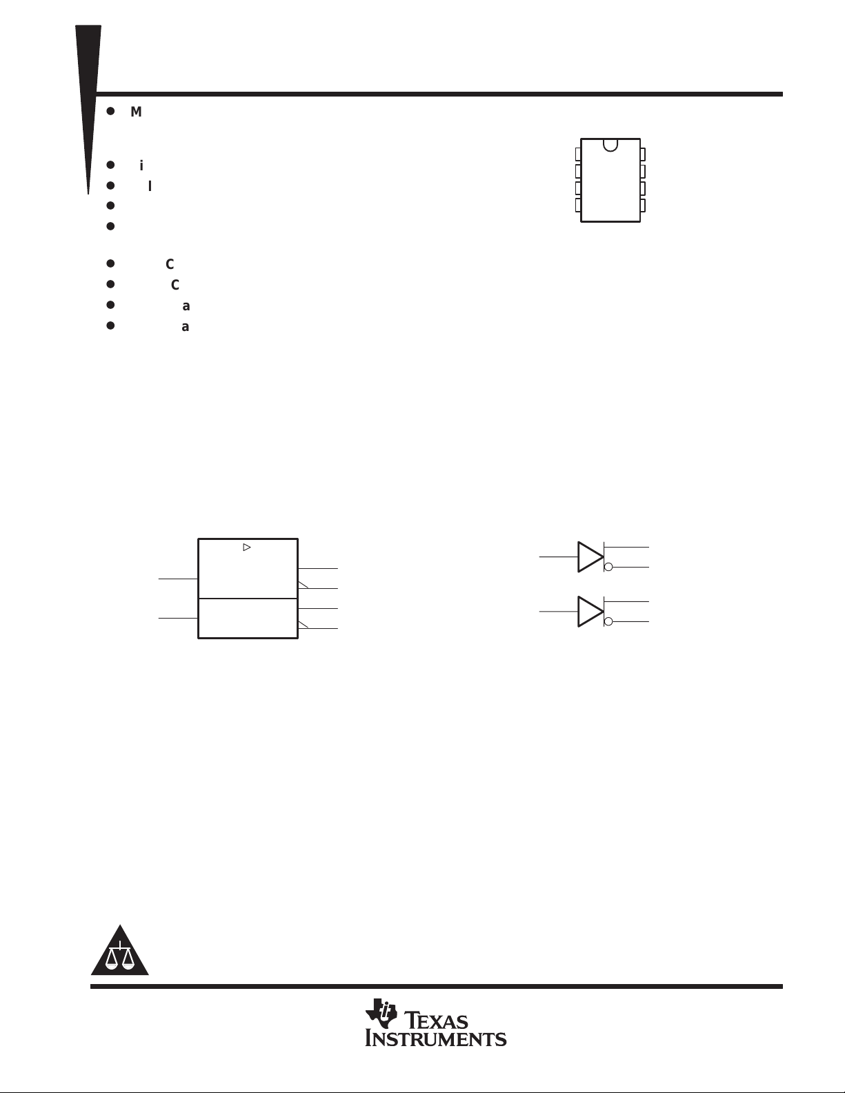
D, P, OR PS† PACKAGE
(TOP VIEW)
1Z
1
1Y
2
1A
3
GND
The PS package is only available left-end
taped and reeled, i.e., order SN75158PSLE.
4
V
8
CC
2Z
7
2Y
6
2A
5
description
The SN75158 is a dual differential line driver designed to satisfy the requirements set by the ANSI
EIA/TIA-422-B and ITU V.11 interface specifications. The outputs provide complementary signals with
high-current capability for driving balanced lines, such as twisted pair, at normal line impedance without high
power dissipation. The output stages are TTL totem-pole outputs providing a high-impedance state in the
power-off condition.
The SN75158 is characterized for operation from 0°C to 70°C.
logic symbol
‡
logic diagram (positive logic)
3
1A
5
2A
‡
This symbol is in accordance with ANSI/IEEE Std 91-1984
and IEC Publication 617-12.
2
1Y
1
1Z
6
2Y
7
2Z
3
1A
5
2A 7
2
1Y
1
1Z
6
2Y
2Z
Please be aware that an important notice concerning availability, standard warranty, and use in critical applications of
Texas Instruments semiconductor products and disclaimers thereto appears at the end of this data sheet.
PRODUCTION DATA information is current as of publication date.
Products conform to specifications per the terms of Texas Instruments
standard warranty. Production processing does not necessarily include
testing of all parameters.
POST OFFICE BOX 655303 • DALLAS, TEXAS 75265
Copyright 1995, Texas Instruments Incorporated
1
SN75158
PACKAGE
A
DUAL DIFFERENTIAL LINE DRIVER
SLLS085B – JANUARY 1977 – REVISED MA Y 1995
schematics of inputs and outputs
EQUIVALENT OF EACH INPUT
V
CC
4 kΩ
NOM
Input
GND
absolute maximum ratings over operating free-air temperature range (unless otherwise noted)
Supply voltage, V
Input voltage, V
(see Note 1) 7 V. . . . . . . . . . . . . . . . . . . . . . . . . . . . . . . . . . . . . . . . . . . . . . . . . . . . . . . . . . . . .
CC
5.5 V. . . . . . . . . . . . . . . . . . . . . . . . . . . . . . . . . . . . . . . . . . . . . . . . . . . . . . . . . . . . . . . . . . . . . . . . . .
I
TYPICAL OF ALL OUTPUTS
V
CC
9 Ω NOM
Output
GND
†
Continuous total power dissipation See Dissipation Rating Table. . . . . . . . . . . . . . . . . . . . . . . . . . . . . . . . . . . . .
Operating free-air temperature range, T
Storage temperature range, T
–65°C to 150°C. . . . . . . . . . . . . . . . . . . . . . . . . . . . . . . . . . . . . . . . . . . . . . . . . . .
stg
0°C to 70°C. . . . . . . . . . . . . . . . . . . . . . . . . . . . . . . . . . . . . . . . . . . . . .
A
Lead temperature 1,6 mm (1/16 inch) from case for 10 seconds 260°C. . . . . . . . . . . . . . . . . . . . . . . . . . . . . . .
†
Stresses beyond those listed under “absolute maximum ratings” may cause permanent damage to the device. These are stress ratings only, and
functional operation of the device at these or any other conditions beyond those indicated under “recommended operating conditions” is not
implied. Exposure to absolute-maximum-rated conditions for extended periods may affect device reliability.
NOTE 1: All voltage values, except differential output voltage VOD, are with respect to network ground terminal. VOD is at the Y output with respect
to the Z output.
POWER RATING ABOVE TA = 25°CAPOWER RATING
D 725 mW 5.8 mW/°C 464 mW
P 1000 mW 8.0 mW/°C 640 mW
PS 450 mW 3.6 mW/°C 288 mW
recommended operating conditions
Supply voltage, V
High-level input voltage, V
Low-level input voltage, V
High-level output current, I
Low-level output current, I
Operating free-air temperature, T
CC
IH
IL
OH
OL
A
DISSIPATION RATING TABLE
TA ≤ 25°C DERATING FACTOR TA = 70°C
MIN NOM MAX UNIT
4.75 5 5.25 V
2 V
0.8 V
–40 mA
40 mA
0 70 °C
2
POST OFFICE BOX 655303 • DALLAS, TEXAS 75265
VOHHigh-level output voltage
CC
,
IL
,
2.43V
VOLLow-level output voltage
CC
,
IL
,
0.2
0.4
V
V
C
¶
V
∆V
gg
CC
±0.02
±0.4
V
ICCSupply current (both drivers)
CC
3750mA
See Figure 2, Termination A
See Figure 2, Termination B
See Figure 2, Termination A
SN75158
DUAL DIFFERENTIAL LINE DRIVER
SLLS085B – JANUARY 1977 – REVISED MA Y 1995
electrical characteristics over operating free-air temperature range (unless otherwise noted)
= 0.8 V,
= 0.8 V,
†
MIN
PARAMETER
V
IK
V
|V
∆V
OC
I
O
I
I
I
IH
I
IL
I
OS
†
For conditions shown as MIN or MAX, use the appropriate value specified under recommended operating conditions.
‡
All typical values are at VCC = 5 V and TA = 25°C except for VOC, for which VCC is as stated under test conditions.
§
∆VOD and ∆|VOC| are the changes in magnitudes of VOD and VOC, respectively, that occur when the input is changed from a high level to a low
level.
¶
In ANSI Standard EIA/TIA-422-B, VOC, which is the average of the two output voltages with respect to ground, is called output offset voltage,
VOS.
#
Only one output should be shorted at a time, and duration of the short circuit should not exceed one second.
Input clamp voltage VCC = MIN, II = –12 mA –0.9 –1.5 V
p
p
| Differential output voltage VCC = MAX, IO = 0 3.5 2×V
OD1
| Differential output voltage VCC = MIN 2 3 V
OD2
Change in magnitude of differential output voltage
OD
ommon-mode output voltage
Change in magnitude of common-mode output V
OC
§
voltage
Output current with power off VCC = 0
Input current at maximum input voltage VCC = MAX, VI = 5.5 V 1 mA
High-level input current VCC = MAX, VI = 2.4 V 40 µA
Low-level input current VCC = MAX, VI = 0.4 V –1 –1.6 mA
Short-circuit output current
pp
#
§
TEST CONDITIONS
V
= MIN, V
VIH = 2 V,
V
= MIN, V
VIH = 2 V,
VCC = MIN ±0.02 ±0.4 V
VCC = MAX
VCC = MIN
= MIN
or MAX
VCC = MAX –40 –90 –150 mA
VCC = MAX, Inputs grounded,
TA = 25°C,gNo load
IOH = –40 mA
IOL = 40 mA
RL = 100 Ω,
See Figure 1
VO = 6 V 0.1 100
VO = – 0.25 V –0.1 –100
VO = – 0.25 to 6 V ±100
‡
TYP
1.8 3
1.5 3
MAX UNIT
OD2
V
µA
switching characteristics, VCC = 5 V, TA = 25°C
t
PLH
t
PHL
t
PLH
t
PHL
t
TLH
t
TLH
PARAMETER TEST CONDITIONS MIN TYP MAX UNIT
Propagation delay time, low-to-high-level output
Propagation delay time, high-to-low-level output
Propagation delay time, low-to-high-level output
Propagation delay time, high-to-low-level output
Transition time, low-to-high-level output
Transition time, high-to-low-level output
Overshoot factor See Figure 2, Termination C 10%
POST OFFICE BOX 655303 • DALLAS, TEXAS 75265
16 25 ns
10 20 ns
13 20 ns
9 15 ns
4 20 ns
4 20 ns
3

SN75158
DUAL DIFFERENTIAL LINE DRIVER
SLLS085B – JANUARY 1977 – REVISED MA Y 1995
PARAMETER MEASUREMENT INFORMATION
Figure 1. Differential and Common-Mode Output Voltages
Input
V
OD2
50 Ω
50 Ω
V
OC
Y
100 Ω
Z
Input
Differential
Output
≤ 5 ns
10%
t
PLH
CL = 30 pF
(see Note B)
90%
50%
50%
Pulse
Generator
(see Note A)
≤ 5 ns
90%
50%
90%
90%
Y
Z
CL = 15 pF
(see Note B)
TERMINATION BTERMINATION A
TEST CIRCUITS
10%
CL = 15 pF
(see Note B)
t
PHL
50%
10%10%
3 V
0 V
Y Output
Z Output
Y
100 Ω
Z
TERMINATION C
Overshoot
100%
0%
t
TLH
NOTES: A. The pulse generator has the following characteristics: ZO = 50 Ω, tw = 25 ns, PRR ≤ 10 MHz.
B. CL includes probe and jig capacitance.
t
THL
VOLTAGE WAVEFORMS
Overshoot
Figure 2. Test Circuit and Voltage Waveforms
4
POST OFFICE BOX 655303 • DALLAS, TEXAS 75265

SN75158
DUAL DIFFERENTIAL LINE DRIVER
SLLS085B – JANUARY 1977 – REVISED MA Y 1995
TYPICAL CHARACTERISTICS
6
5
4
3
2
O
V
VO – Output Voltage – V
1
0
0
5
OUTPUT VOLTAGE
vs
DATA INPUT VOLTAGE
No Load
TA = 25°C
VCC = 5.5 V
VCC = 5 V
VCC = 4.5 V
1 2 3 4
VI – Data Input Voltage – V
Figure 3
HIGH-LEVEL OUTPUT VOLTAGE
vs
HIGH-LEVEL OUTPUT CURRENT
TA = 25°C
6
5
4
3
2
O
V
VO – Output Voltage – V
1
0
0
0.4
OUTPUT VOLTAGE
vs
DATA INPUT VOLTAGE
VCC = 5 V
No Load
TA = – 55°C
VI – Data Input Voltage – V
Figure 4
LOW-LEVEL OUTPUT VOLTAGE
vs
LOW-LEVEL OUTPUT CURRENT
TA = 25°C
TA = 125°C
TA = 25°C
321
4
4
3
2
1
OH
V
VOH – High-Level Output Voltage – V
0
0
VCC = 5.5 V
VCC = 5 V
VCC = 4.5 V
–20 –40 –60 –80 –100
IOH – High-Level Output Current – mA
Figure 5
–120
0.3
0.2
0.1
OL
V
VOL – Low-Level Output Voltage – V
0
0
VCC = 5.5 V
VCC = 4.5 V
10 20 30 40 50 60 70
IOL – Low-Level Output Current – mA
Figure 6
80
POST OFFICE BOX 655303 • DALLAS, TEXAS 75265
5

SN75158
DUAL DIFFERENTIAL LINE DRIVER
SLLS085B – JANUARY 1977 – REVISED MA Y 1995
TYPICAL CHARACTERISTICS
4
3.5
3
2.5
2
1.5
O
VO – Output Voltage – V
V
1
0.5
0
–75
80
70
60
50
40
OUTPUT VOLTAGE
vs
FREE-AIR TEMPERATURE
VCC = 5 V
VOH(IOH = –20 mA)
VOH(IOH = –40 mA)
VOL(IOL = 40 mA)
–50 –25 0 25 50 75 100
TA – Free-Air Temperature – ° C
Figure 7
SUPPLY CURRENT
(BOTH DRIVERS)
vs
SUPPLY VOLTAGE
No Load
TA = 25°C
Inputs Grounded
125
30
25
20
15
10
pd
t
5
tpd – Propagation Delay Times – ns
0
–75
42
40
38
36
PROPAGATION DELAY TIMES
vs
FREE-AIR TEMPERATURE
VCC = 5 V
See Figure 2
Termination A
t
PLH
t
PHL
–50 –25 0 25 50 75 100
TA – Free-Air Temperature – ° C
Figure 8
SUPPLY CURRENT
(BOTH DRIVERS)
vs
FREE-AIR TEMPERATURE
VCC = 5 V
Input Grounded
Outputs Open
125
30
CC
ICC – Supply Current – mA
20
I
10
0
0
1 2 3 4 5 6 7
6
Inputs Open
VCC – Supply Voltage – V
Figure 9
POST OFFICE BOX 655303 • DALLAS, TEXAS 75265
34
CC
ICC – Supply Current – mA
I
32
30
– 75 125
8
–50 –25 0 25 50 75 100
TA – Free-Air Temperature – ° C
Figure 10

SN75158
DUAL DIFFERENTIAL LINE DRIVER
SLLS085B – JANUARY 1977 – REVISED MA Y 1995
TYPICAL CHARACTERISTICS
SUPPLY CURRENT
(BOTH DRIVERS)
vs
FREQUENCY
100
VCC = 5 V
∞
RL =
CL = 30 pF
80
Inputs: 3-V Square Wave
TA = 25°C
60
40
CC
ICC – Supply Current – mA
I
20
0
0.1
0.4 1 4 10 40
f – Frequency – MHz
100
Figure 11
POST OFFICE BOX 655303 • DALLAS, TEXAS 75265
7

IMPORTANT NOTICE
T exas Instruments and its subsidiaries (TI) reserve the right to make changes to their products or to discontinue
any product or service without notice, and advise customers to obtain the latest version of relevant information
to verify, before placing orders, that information being relied on is current and complete. All products are sold
subject to the terms and conditions of sale supplied at the time of order acknowledgement, including those
pertaining to warranty, patent infringement, and limitation of liability.
TI warrants performance of its semiconductor products to the specifications applicable at the time of sale in
accordance with TI’s standard warranty. Testing and other quality control techniques are utilized to the extent
TI deems necessary to support this warranty . Specific testing of all parameters of each device is not necessarily
performed, except those mandated by government requirements.
CERT AIN APPLICATIONS USING SEMICONDUCTOR PRODUCTS MAY INVOLVE POTENTIAL RISKS OF
DEATH, PERSONAL INJURY, OR SEVERE PROPERTY OR ENVIRONMENTAL DAMAGE (“CRITICAL
APPLICATIONS”). TI SEMICONDUCTOR PRODUCTS ARE NOT DESIGNED, AUTHORIZED, OR
WARRANTED TO BE SUITABLE FOR USE IN LIFE-SUPPORT DEVICES OR SYSTEMS OR OTHER
CRITICAL APPLICA TIONS. INCLUSION OF TI PRODUCTS IN SUCH APPLICATIONS IS UNDERST OOD TO
BE FULLY AT THE CUSTOMER’S RISK.
In order to minimize risks associated with the customer’s applications, adequate design and operating
safeguards must be provided by the customer to minimize inherent or procedural hazards.
TI assumes no liability for applications assistance or customer product design. TI does not warrant or represent
that any license, either express or implied, is granted under any patent right, copyright, mask work right, or other
intellectual property right of TI covering or relating to any combination, machine, or process in which such
semiconductor products or services might be or are used. TI’s publication of information regarding any third
party’s products or services does not constitute TI’s approval, warranty or endorsement thereof.
Copyright 1998, Texas Instruments Incorporated
 Loading...