

SN75154
QUADRUPLE LINE RECEIVER
SLLS083B – NOVEMBER 1970 – REVISED MA Y 1995
1
POST OFFICE BOX 655303 • DALLAS, TEXAS 75265
D
Meets or Exceeds the Requirements of
ANSI Standard EIA/TIA-232-E and ITU
Recommendation V.28
D
Input Resistance . . . 3 kΩ to 7 kΩ Over Full
EIA/TIA-232-E V oltage Range
D
Input Threshold Adjustable to Meet
Fail-Safe Requirements Without Using
External Components
D
Built-In Hysteresis for Increased Noise
Immunity
D
Inverting Output Compatible With TTL
D
Output With Active Pullup for Symmetrical
Switching Speeds
D
Standard Supply Voltages ...5 V or 12 V
description
The SN75154 is a monolithic low-power Schottky line receiver designed to satisfy the requirements of the
standard interface between data terminal equipment and data communication equipment as defined by ANSI
Standard EIA/TIA-232-E. Other applications are for relatively short, single-line, point-to-point data transmission
and for level translators. Operation is normally from a single 5-V supply; however, a built-in option allows
operation from a 12-V supply without the use of additional components. The output is compatible with most TTL
circuits when either supply voltage is used.
In normal operation, the threshold-control terminals are connected to the V
CC1
terminal, even if power is being
supplied via the alternate V
CC2
terminal. This provides a wide hysteresis loop, which is the difference between
the positive-going and negative-going threshold voltages. See typical characteristics. In this mode of operation,
if the input voltage goes to zero, the output voltage will remain at the low or high level as determined by the
previous input.
For fail-safe operation, the threshold-control terminals are open. This reduces the hysteresis loop by causing
the negative-going threshold voltage to be above zero. The positive-going threshold voltage remains above
zero as it is unaffected by the disposition of the threshold terminals. In the fail-safe mode, if the input voltage
goes to zero or an open-circuit condition, the output will go to the high level regardless of the previous input
condition.
The SN75154 is characterized for operation from 0°C to 70°C.
Copyright 1995, Texas Instruments Incorporated
PRODUCTION DATA information is current as of publication date.
Products conform to specifications per the terms of Texas Instruments
standard warranty. Production processing does not necessarily include
testing of all parameters.
Please be aware that an important notice concerning availability, standard warranty, and use in critical applications of
Texas Instruments semiconductor products and disclaimers thereto appears at the end of this data sheet.
1
2
3
4
5
6
7
8
16
15
14
13
12
11
10
9
3T
2T
1T
1A
2A
3A
4A
GND
V
CC2
V
CC1
4T
1Y
2Y
3Y
4Y
R1
†
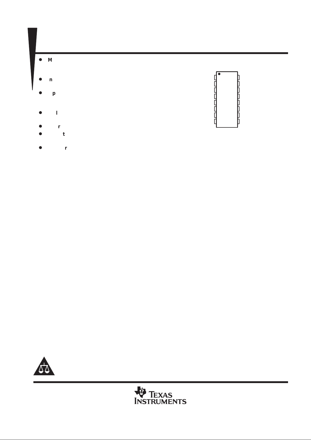
(TOP VIEW)
D OR N PACKAGE
†
For function of R1, see schematic
SN75154
QUADRUPLE LINE RECEIVER
SLLS083B – NOVEMBER 1970 – REVISED MA Y 1995
2
POST OFFICE BOX 655303 • DALLAS, TEXAS 75265
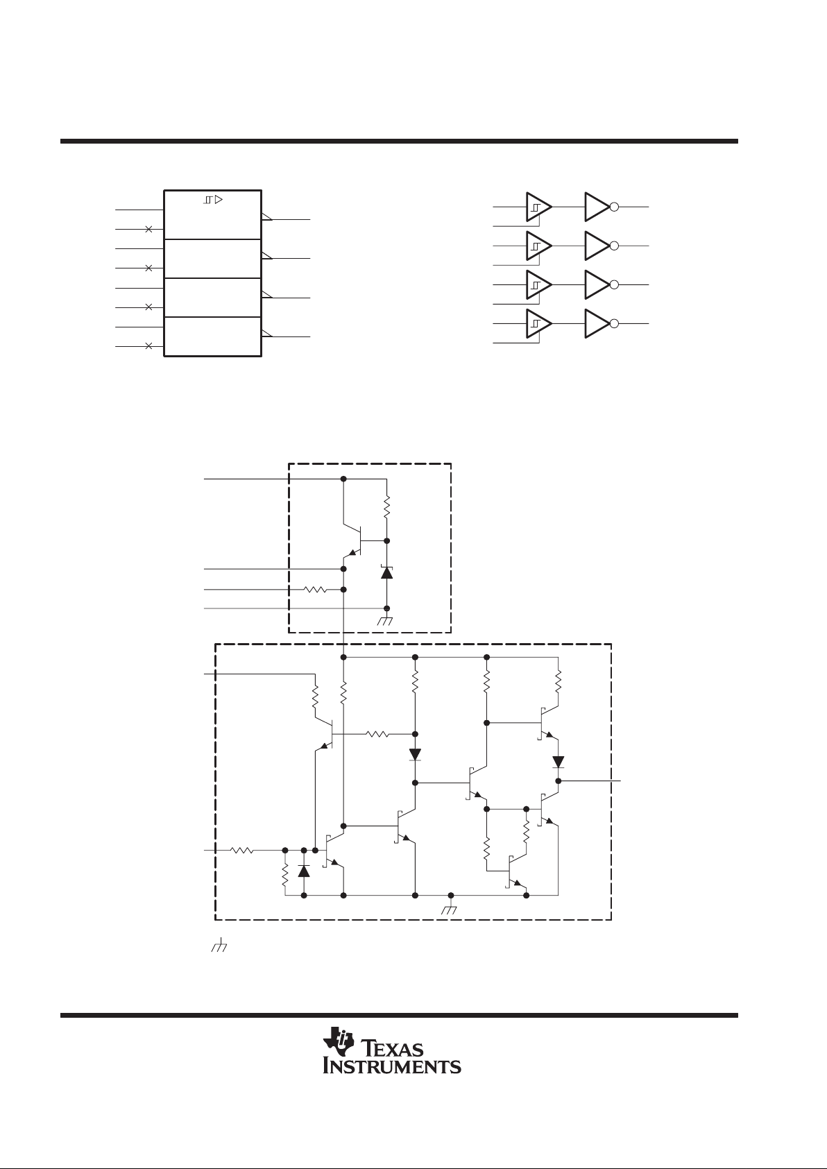
logic symbol
†
THRS ADJ
4T
4A
3T
3A
2T
2A
1T
1A
10
11
12
13
4Y
3Y
2Y
1Y
14
7
1
6
2
5
3
4
†
This symbol is in accordance with ANSI/IEEE Std 91-1984
and IEC Publication 617-12.
logic diagram (positive logic)
14
7
1
6
2
5
3
4
4T
4A
3T
3A
2T
2A
1T
1A
10
11
12
13
4Y
3Y
2Y
1Y
schematic
Component values shown are nominal.
V
CC2
‡
V
CC1
R1
GND
Threshold
Input
Control
Common to Four Receivers
1 of 4 Receivers
5 kΩ
3.2 kΩ
5.5 kΩ
5 kΩ
1.6 kΩ 1.6 kΩ 200 Ω
4.2 kΩ
2.7 kΩ
1 kΩ
240 Ω
Output
9.9 kΩ
. . . Substrate
‡
When V
CC1
is used, V
CC2
may be left open or shorted to V
CC1
. When V
CC2
is used, V
CC1
must be left open
or connected to the threshold control pins.
SN75154
QUADRUPLE LINE RECEIVER
SLLS083B – NOVEMBER 1970 – REVISED MA Y 1995
3
POST OFFICE BOX 655303 • DALLAS, TEXAS 75265
absolute maximum ratings over operating free-air temperature range (unless otherwise noted)
†
Normal supply voltage, V
CC1
(see Note 1) 7 V. . . . . . . . . . . . . . . . . . . . . . . . . . . . . . . . . . . . . . . . . . . . . . . . . . . . .
Alternate supply voltage, V
CC2
14 V. . . . . . . . . . . . . . . . . . . . . . . . . . . . . . . . . . . . . . . . . . . . . . . . . . . . . . . . . . . . . .
Input voltage, V
I
±25 V. . . . . . . . . . . . . . . . . . . . . . . . . . . . . . . . . . . . . . . . . . . . . . . . . . . . . . . . . . . . . . . . . . . . . . . . . .
Continuous total power dissipation See Dissipation Rating Table. . . . . . . . . . . . . . . . . . . . . . . . . . . . . . . . . . . . .
Operating free-air temperature range, T
A
0°C to 70°C. . . . . . . . . . . . . . . . . . . . . . . . . . . . . . . . . . . . . . . . . . . . . .
Storage temperature range, T
stg
–65°C to 150°C. . . . . . . . . . . . . . . . . . . . . . . . . . . . . . . . . . . . . . . . . . . . . . . . . . .
Lead temperature 1,6 mm (1/16 inch) from case for 10 seconds 260°C. . . . . . . . . . . . . . . . . . . . . . . . . . . . . . .
†
Stresses beyond those listed under “absolute maximum ratings” may cause permanent damage to the device. These are stress ratings only, and
functional operation of the device at these or any other conditions beyond those indicated under “recommended operating conditions” is not
implied. Exposure to absolute-maximum-rated conditions for extended periods may affect device reliability.
NOTE 1: Voltage values are with respect to network GND terminal.
DISSIPATION RATING TABLE
T
≤ 25°C DERATING FACTOR T
= 70°C
PACKAGE
A
POWER RATING ABOVE TA = 25°CAPOWER RATING
D 950 mW 7.6 mW/°C 608 mW
N 1150 mW 9.2 mW/°C 736 mW
NS 625 mW 5.0 mW/°C 400 mW
recommended operating conditions
MIN NOM MAX UNIT
Normal supply voltage, V
CC1
4.5 5 5.5 V
Alternate supply voltage, V
CC2
10.8 12 13.2 V
High-level input voltage, VIH (see Note 2) 3 15 V
Low-level input voltage, VIL (see Note 2) –15 –3 V
High-level output current, I
OH
–400 µA
Low-level output current, I
OL
16 mA
Operating free-air temperature, T
A
0 70 °C
NOTE 2: The algebraic convention, where the less positive (more negative) limit is designated as minimum, is used in this data sheet for logic
and threshold levels only, e.g., when 0 V is the maximum, the minimum limit is a more negative voltage.

SN75154
QUADRUPLE LINE RECEIVER
SLLS083B – NOVEMBER 1970 – REVISED MA Y 1995
4
POST OFFICE BOX 655303 • DALLAS, TEXAS 75265
electrical characteristics over recommended operating free-air temperature range (unless
otherwise noted)
TEST
PARAMETER
FIGURE
TEST CONDITIONS
MIN
TYP†MAX
UNIT
Positive-going input
Normal operation
0.8 2.2 3
V
IT+
gg
threshold voltage
Fail-safe operation
1
0.8 2.2 3
V
Negative-going input
Normal operation
–3 –1.1 0
V
IT–
ggg
threshold voltage
Fail-safe operation
1
0.8 1.4 3
V
Hysteresis voltage
Normal operation
0.8 3.3 6
V
hys
yg
(V
IT+
– V
IT–
)
Fail-safe operation
1
0 0.8 2.2
V
V
OH
High-level output voltage 1 IOH = –400 µA 2.4 3.5 V
V
OL
Low-level output voltage 1 IOL = 16 mA 0.29 0.4 V
∆VI = –25 V to –14 V 3 5 7
∆VI = –14 V to –3 V 3 5 7
r
i
Input resistance 2
∆VI = –3 V to 3 V 3 6 8
∆VI = 3 V to 14 V 3 5 7
kΩ
∆VI = 14 V to 25 V 3 5 7
V
I(open)
Open-circuit input voltage 3 II = 0 0 0.2 2 V
I
OS
Short-circuit output current
‡
4 V
CC1
= 5.5 V, VI = –5 V –10 –20 –40 mA
I
CC1
Supply current from V
CC1
V
CC1
= 5.5 V, TA = 25°C 20 35
I
CC2
Supply current from V
CC2
5
V
CC2
= 13.2 V , TA = 25°C 23 40
mA
†
All typical values are at V
CC1
= 5 V, TA = 25°C.
‡
Not more than one output should be shorted at a time.
switching characteristics, V
CC1
= 5 V, TA = 25°C, N = 10
TEST
PARAMETER
FIGURE
TEST CONDITIONS
MIN
TYP
MAX
UNIT
t
PLH
Propagation delay time, low- to high-level output 11 ns
t
PHL
Propagation delay time, high- to low-level output
p
8 ns
t
TLH
Transition time, low- to high-level output
6
C
L
= 50 pF,
R
L
=
390 Ω
7 ns
t
THL
Transition time, high- to low-level output 2.2 ns

SN75154
QUADRUPLE LINE RECEIVER
SLLS083B – NOVEMBER 1970 – REVISED MA Y 1995
5
POST OFFICE BOX 655303 • DALLAS, TEXAS 75265
TYPICAL CHARACTERISTICS
4
3
2
1
0
–4 –3 –2 –1 0 1 2 3 4 25–25
VI – Input Voltage – V
VO – Output Voltage – V
V
CC1
= 5 V
TA = 25°C
Normal
Operation Operation
Fail-Safe
See Note A
V
IT–
V
IT–
V
IT+
V
O
OUTPUT VOLTAGE
vs
INPUT VOLTAGE
NOTE A: For normal operation, the threshold controls are connected to V
CC1
. For fail-safe
operation, the threshold controls are open.
Figure 1

SN75154
QUADRUPLE LINE RECEIVER
SLLS083B – NOVEMBER 1970 – REVISED MA Y 1995
6
POST OFFICE BOX 655303 • DALLAS, TEXAS 75265
PARAMETER MEASUREMENT INFORMATION
dc test circuits
†
TEST TABLE
TEST
MEASURE A T Y V
CC1
V
CC2
p
p
V
OH
Open Open I
OH
4.5 V Open
Open-circuit input (fail safe)
V
OH
Open Open I
OH
Open 10.8 V
V
OH
0.8 V Open I
OH
5.5 V Open
V
IT+
min, V
IT–
min (fail safe)
V
OH
0.8 V Open I
OH
Open 13.2 V
V
OH
Note A V
CC1
I
OH
5.5 V and T Open
V
IT+
min (normal)
V
OH
Note A V
CC1
I
OH
T 13.2 V
V
OH
–3 V V
CC1
I
OH
5.5 V and T Open
V
IL
ma
x,
V
IT+
min (normal)
V
OH
–3 V V
CC1
I
OH
T 13.2 V
V
OL
3 V Open I
OL
4.5 V Open
V
IH
min, V
IT+
max,
V
IT–
max
(fail safe)
V
OL
3 V Open I
OL
Open 10.8 V
V
OL
3 V V
CC1
I
OL
4.5 V and T Open
V
IH
min, V
IT+
max
(normal)
V
OL
3 V V
CC1
I
OL
T 10.8 V
V
OL
Note B V
CC1
I
OL
5.5 V and T Open
V
IT–
max (normal)
V
OL
Note B V
CC1
I
OL
T 13.2 V
NOTES: A. Momentarily apply –5 V, then 0.8 V.
B. Momentarily apply 5 V, then GND.
V
OL
V
OH
GND
Open
VI,V
IT
5.5 V
Open
4.5 V
T
A
13.2 V
Open
10.8 V
I
OL
Y
R1V
CC2
V
CC1
I
OH
Figure 2. VIH, VIL, V
IT+
, V
IT –
, VOH, V
OL
†
Arrows indicate actual direction of current flow. Current into a terminal is a positive value.

V
CC1
V
CC2
R1
Y
Open
12 V
A
T
Open
5 V
V
I
Open
GND
I
I
Open
V
I
I
I
ri =
Open
GND
Open
5.5 V
T
A
13.2 V
Y
R1
V
CC2
V
CC1
V
I(open)
SN75154
QUADRUPLE LINE RECEIVER
SLLS083B – NOVEMBER 1970 – REVISED MA Y 1995
7
POST OFFICE BOX 655303 • DALLAS, TEXAS 75265
PARAMETER MEASUREMENT INFORMATION
dc test circuits
†
(continued)
TEST TABLE
T
V
CC1
V
CC2
Open 5 V Open
Open GND Open
Open Open Open
V
CC1
T and 5 V Open
GND GND Open
Open Open 12 V
Open Open GND
V
CC1
T 12 V
V
CC1
T GND
V
CC1
T Open
Figure 3. Input Resistance
TEST TABLE
T
V
CC1
V
CC2
Open 5.5 V Open
V
CC1
5.5 V Open
Open Open 13.2 V
V
CC1
T 13.2 V
Figure 4. Input Voltage (Open)
V
CC1
V
CC2
R1
Y
13.2 V
A
T
5.5 V
Open
GND
V
CC1
V
CC2
R1
YA
Open
GND
I
OS
–5 V
Open5.5 VOpen
5 V
Open
I
CC1
I
CC2
Each output is tested separately.
All four line receivers are tested simultaneously.
Open
Figure 5. Output Short-Circuit Current Figure 6. Supply Current
†
Arrows indicate actual direction of current flow. Current into a terminal is a positive value.

SN75154
QUADRUPLE LINE RECEIVER
SLLS083B – NOVEMBER 1970 – REVISED MA Y 1995
8
POST OFFICE BOX 655303 • DALLAS, TEXAS 75265
PARAMETER MEASUREMENT INFORMATION
V
CC1
V
CC2
R1
YA
T
Open
GND
Pulse
Generator
(see Note A)
Output
5 VInput
Open
RL = 390 Ω
See Note C
CL = 50 pF
(see Note B)
TEST CIRCUIT
t
PHL
10 ± 2 ns
90%
3 V
10%
3 V
90%
10%
10 ± 2 ns
t
PLH
Input
Output
t
THL
2 V
1.5 V
0.8 V 0.8 V
1.5 V
2 V
t
TLH
5 V
0 V
–5 V
V
OH
V
OL
VOLTAGE W AVEFORMS
NOTES: A. The pulse generator has the following characteristics: ZO = 50 Ω, tw ≤ 200 ns, duty cycle ≤ 20%.
B. CL includes probe and jig capacitance.
C. All diodes are 1N3064.
Figure 6. Test Circuit and Voltage Waveforms

IMPORTANT NOTICE
T exas Instruments and its subsidiaries (TI) reserve the right to make changes to their products or to discontinue
any product or service without notice, and advise customers to obtain the latest version of relevant information
to verify, before placing orders, that information being relied on is current and complete. All products are sold
subject to the terms and conditions of sale supplied at the time of order acknowledgement, including those
pertaining to warranty, patent infringement, and limitation of liability.
TI warrants performance of its semiconductor products to the specifications applicable at the time of sale in
accordance with TI’s standard warranty. Testing and other quality control techniques are utilized to the extent
TI deems necessary to support this warranty. Specific testing of all parameters of each device is not necessarily
performed, except those mandated by government requirements.
CERT AIN APPLICATIONS USING SEMICONDUCTOR PRODUCTS MAY INVOLVE POTENTIAL RISKS OF
DEATH, PERSONAL INJURY, OR SEVERE PROPERTY OR ENVIRONMENTAL DAMAGE (“CRITICAL
APPLICATIONS”). TI SEMICONDUCTOR PRODUCTS ARE NOT DESIGNED, AUTHORIZED, OR
WARRANTED TO BE SUITABLE FOR USE IN LIFE-SUPPORT DEVICES OR SYSTEMS OR OTHER
CRITICAL APPLICATIONS. INCLUSION OF TI PRODUCTS IN SUCH APPLICA TIONS IS UNDERST OOD TO
BE FULLY AT THE CUSTOMER’S RISK.
In order to minimize risks associated with the customer’s applications, adequate design and operating
safeguards must be provided by the customer to minimize inherent or procedural hazards.
TI assumes no liability for applications assistance or customer product design. TI does not warrant or represent
that any license, either express or implied, is granted under any patent right, copyright, mask work right, or other
intellectual property right of TI covering or relating to any combination, machine, or process in which such
semiconductor products or services might be or are used. TI’s publication of information regarding any third
party’s products or services does not constitute TI’s approval, warranty or endorsement thereof.
Copyright 1998, Texas Instruments Incorporated
 Loading...