SN75150
DUAL LINE DRIVER
SLLS081C – JANUARY 1971 – REVISED JUNE 1999
1
POST OFFICE BOX 655303 • DALLAS, TEXAS 75265
D
Meets or Exceeds the Requirement of
TIA/EIA-232-F and ITU Recommendation
V.28
D
Withstands Sustained Output Short Circuit
to Any Low-Impedance Voltage Between
–25 V and 25 V
D
2-µs Maximum Transition Time Through the
3-V to –3-V Transition Region Under Full
2500-pF Load
D
Inputs Compatible With Most TTL Families
D
Common Strobe Input
D
Inverting Output
D
Slew Rate Can Be Controlled With an
External Capacitor at the Output
D
Standard Supply Voltages . . . ±12 V
description
The SN75150 is a monolithic dual line driver designed to satisfy the requirements of the standard interface
between data-terminal equipment and data-communication equipment as defined by TIA/EIA-232-F. A rate of
20 kbits/s can be transmitted with a full 2500-pF load. Other applications are in data-transmission systems using
relatively short single lines, in level translators, and for driving MOS devices. The logic input is compatible with
most TTL families. Operation is from 12-V and –12-V power supplies.
The SN75150 is characterized for operation from 0°C to 70°C.
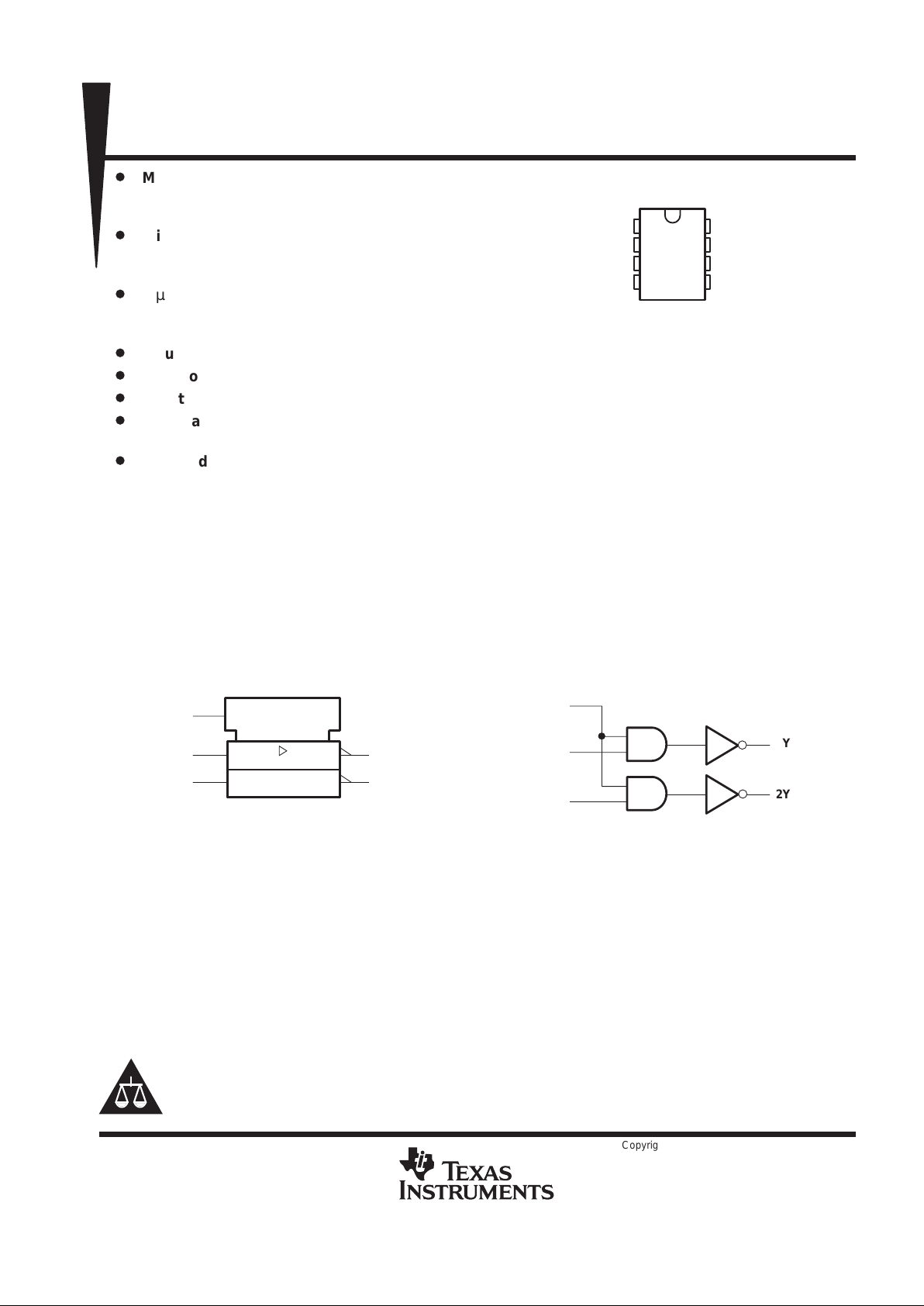
logic symbol
†
7
6
†
This symbol is in accordance with ANSI/IEEE Std 91-1984
and IEC Publication 617-12.
EN
1Y
2Y
S
1A
2A
3
2
1
logic diagram (positive logic)
3
2
1
S
1A
2A
7
6
1Y
2Y
Copyright 1999, Texas Instruments Incorporated
PRODUCTION DATA information is current as of publication date.
Products conform to specifications per the terms of Texas Instruments
standard warranty. Production processing does not necessarily include
testing of all parameters.
Please be aware that an important notice concerning availability, standard warranty, and use in critical applications of
Texas Instruments semiconductor products and disclaimers thereto appears at the end of this data sheet.
1
2
3
4
8
7
6
5
S
1A
2A
GND
V
CC+
1Y
2Y
V
CC–
D OR P PACKAGE
(TOP VIEW)

SN75150
DUAL LINE DRIVER
SLLS081C – JANUARY 1971 – REVISED JUNE 1999
2
POST OFFICE BOX 655303 • DALLAS, TEXAS 75265
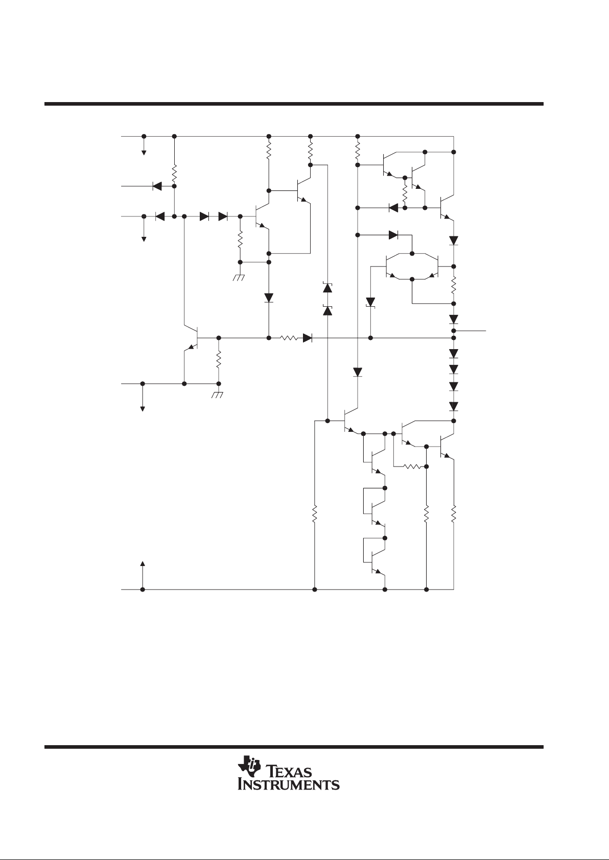
schematic (each line driver)
V
CC–
Line Driver
To Other
GND
Strobe S
To Other
Line Driver
4.5 kΩ
15 kΩ
7 kΩ
V
CC+
Input A
15 kΩ 10 kΩ
15 kΩ
5 kΩ
47 Ω
Output Y
10 kΩ
5 kΩ
1 kΩ
47 Ω
11 kΩ
To Other
Line Driver
Line Driver
To Other
Resistor values shown are nominal.

SN75150
DUAL LINE DRIVER
SLLS081C – JANUARY 1971 – REVISED JUNE 1999
3
POST OFFICE BOX 655303 • DALLAS, TEXAS 75265
absolute maximum ratings over operating free-air temperature range (unless otherwise noted)
†
Supply voltage, V
CC+
(see Note 1) 15 V. . . . . . . . . . . . . . . . . . . . . . . . . . . . . . . . . . . . . . . . . . . . . . . . . . . . . . . . . . .
Supply voltage, V
CC–
–15 V. . . . . . . . . . . . . . . . . . . . . . . . . . . . . . . . . . . . . . . . . . . . . . . . . . . . . . . . . . . . . . . . . . . . .
Input voltage, V
I
15 V. . . . . . . . . . . . . . . . . . . . . . . . . . . . . . . . . . . . . . . . . . . . . . . . . . . . . . . . . . . . . . . . . . . . . . . . . . .
Applied output voltage ±25 V. . . . . . . . . . . . . . . . . . . . . . . . . . . . . . . . . . . . . . . . . . . . . . . . . . . . . . . . . . . . . . . . . . . . .
Package thermal impedance, θ
JA
(see Notes 2 and 3): D package 197°C/W. . . . . . . . . . . . . . . . . . . . . . . . . . .
P package 104°C/W. . . . . . . . . . . . . . . . . . . . . . . . . . . .
Lead temperature 1,6 mm (1/16 inch) from case for 10 seconds 260°C. . . . . . . . . . . . . . . . . . . . . . . . . . . . . . .
Storage temperature range, T
stg
–65°C to 150°C. . . . . . . . . . . . . . . . . . . . . . . . . . . . . . . . . . . . . . . . . . . . . . . . . . .
†
Stresses beyond those listed under “absolute maximum ratings” may cause permanent damage to the device. These are stress ratings only, and
functional operation of the device at these or any other conditions beyond those indicated under “recommended operating conditions” is not
implied. Exposure to absolute-maximum-rated conditions for extended periods may affect device reliability.
NOTES: 1. Voltage values are with respect to network ground terminal.
2. Maximum power dissipation is a function of TJ(max),
θ
JA
, and TA. The maximum allowable power dissipation at any allowable
ambient temperature is PD = (TJ(max) – TA)/
θ
JA
. Operating at the absolute maximum TJ of 150°C can impact reliability.
3. The package thermal impedance is calculated in accordance with JESD 51, except for through-hole packages, which use a trace
length of zero.
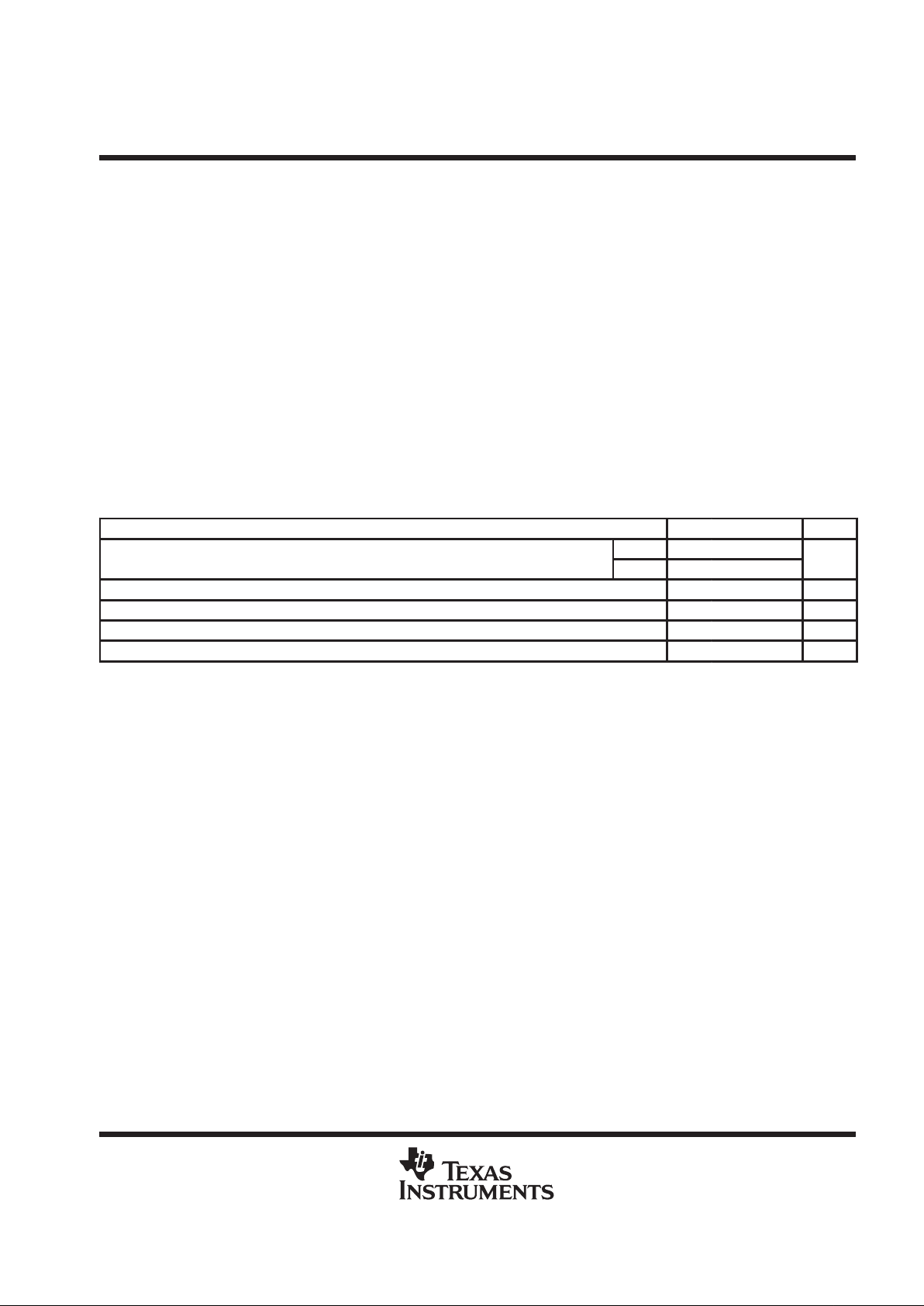
recommended operating conditions
MIN NOM MAX UNIT
pp
V
CC+
10.8 12 13.2
Suppl
y v
oltage
V
CC–
–10.8 –12 –13.2
V
High-level input voltage, V
IH
2 5.5 V
Low-level input voltage, V
IL
0 0.8 V
Driver output voltage, V
O
±15 V
Operating free-air temperature, T
A
0 70 °C
 Loading...