

SN75140
DUAL LINE RECEIVER
SLLS080C – JANUARY 1977 – REVISED APRIL 1998
1
POST OFFICE BOX 655303 • DALLAS, TEXAS 75265
D
Single 5-V Supply
D
±100-mV Sensitivity
D
For Application as:
– Single-Ended Line Receiver
– Gated Oscillator
– Level Comparator
D
Adjustable Reference Voltage
D
TTL Outputs
D
TTL-Compatible Strobe
D
Designed for Party-Line (Data-Bus)
Applications
D
Common Reference-V oltage Pin
D
Common Strobe
description
This device consists of a dual single-ended line receiver with TTL-compatible strobes and outputs. The
reference voltage (switching threshold) is applied externally and can be adjusted from 1.5 V to 3.5 V, making
it possible to optimize noise immunity for a given system design. Due to the low input current (less than 100 µA),
the device is suited ideally for party-line (data-bus) systems.
The SN75140 has a common reference-voltage pin and a common strobe.
The SN75140 is characterized for operation from 0°C to 70°C.
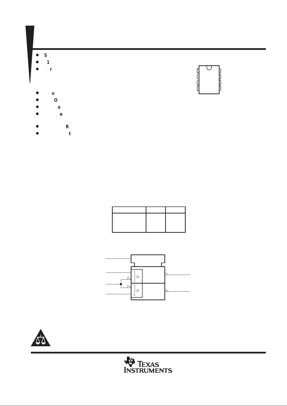
FUNCTION TABLE
(each receiver)
LINE INPUT
STROBE OUTPUT
≤ V
ref
– 100 mV L H
≥ V
ref
+ 100 mV X L
X H L
H = high level, L = low level, X = irrelevant
logic symbol
‡
2
COMSTRB
‡
This symbol is in accordance with ANSI/IEEE Std 91-1984 and IEC Publication 617-12.
3
1LINE
1OUT
1
≥1
5
2LINE
2OUT
7
≥1
6
COMREF
Copyright 1998, Texas Instruments Incorporated
PRODUCTION DATA information is current as of publication date.
Products conform to specifications per the terms of Texas Instruments
standard warranty. Production processing does not necessarily include
testing of all parameters.
Please be aware that an important notice concerning availability, standard warranty, and use in critical applications of
Texas Instruments semiconductor products and disclaimers thereto appears at the end of this data sheet.
1
2
3
4
8
7
6
5
1OUT
COMSTRB
1LINE
GND
V
CC
2OUT
COMREF
2LINE
P OR PS† PACKAGE
(TOP VIEW)
†
The PS package is only available
left-ended taped and reeled (order
SN75140 PSR).
SN75140
DUAL LINE RECEIVER
SLLS080C – JANUARY 1977 – REVISED APRIL 1998
2
POST OFFICE BOX 655303 • DALLAS, TEXAS 75265
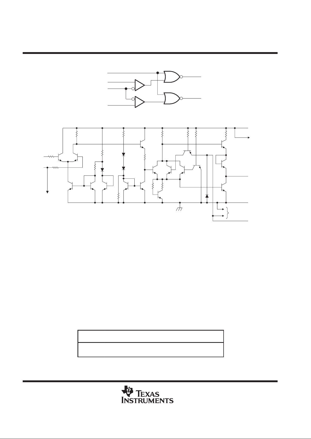
logic diagram (positive logic)
2
3
6
5
1
7
1OUT
2OUT
COMSTRB
1LINE
COMREF
2LINE
schematic (each receiver)
To Other
Line Receiver
V
CC
OUT
COMSTRB
To Other Line Receiver
To Other
Line Receiver
GND
COMREF
LINE
NOTE: Resistor values shown are nominal and in ohms.
1500 750 40001500 4000 130
1500
750
850
470
470
2900
500 1000
absolute maximum ratings over operating free-air temperature range (unless otherwise noted)
†
Supply voltage, V
CC
(see Note 1) 7 V. . . . . . . . . . . . . . . . . . . . . . . . . . . . . . . . . . . . . . . . . . . . . . . . . . . . . . . . . . . . .
Reference input voltage, V
ref
5.5 V. . . . . . . . . . . . . . . . . . . . . . . . . . . . . . . . . . . . . . . . . . . . . . . . . . . . . . . . . . . . . . .
Line input voltage range with respect to GND –2 V to 5.5 V. . . . . . . . . . . . . . . . . . . . . . . . . . . . . . . . . . . . . . . . . .
Line input voltage with respect to V
ref
±5 V. . . . . . . . . . . . . . . . . . . . . . . . . . . . . . . . . . . . . . . . . . . . . . . . . . . . . . . . .
Strobe input voltage 5.5 V. . . . . . . . . . . . . . . . . . . . . . . . . . . . . . . . . . . . . . . . . . . . . . . . . . . . . . . . . . . . . . . . . . . . . . .
Continuous total power dissipation See Dissipation Rating Table. . . . . . . . . . . . . . . . . . . . . . . . . . . . . . . . . . . . .
Storage temperature range, T
stg
–65°C to 150°C. . . . . . . . . . . . . . . . . . . . . . . . . . . . . . . . . . . . . . . . . . . . . . . . . . .
Lead temperature 1,6 mm (1/16 inch) from case for 10 seconds 260°C. . . . . . . . . . . . . . . . . . . . . . . . . . . . . . .
†
Stresses beyond those listed under “absolute maximum ratings” may cause permanent damage to the device. These are stress ratings only, and
functional operation of the device at these or any other conditions beyond those indicated under “recommended operating conditions” is not
implied. Exposure to absolute-maximum-rated conditions for extended periods may affect device reliability.
NOTE 1: Unless otherwise specified, voltage values are with respect to network ground terminal.
DISSIPATION RATING TABLE
PACKAGE
TA ≤ 25°C
POWER RATING
DERATING FACTOR
ABOVE TA = 25°C
TA = 70°C
POWER RATING
P 1000 mW 8.0 mW/°C 640 mW
PS 450 mW 3.6 mW/°C 288 mW
SN75140
DUAL LINE RECEIVER
SLLS080C – JANUARY 1977 – REVISED APRIL 1998
3
POST OFFICE BOX 655303 • DALLAS, TEXAS 75265
recommended operating conditions
MIN NOM MAX UNIT
Supply voltage, V
CC
4.5 5 5.5 V
Reference input voltage, V
ref
1.5 3.5 V
High-level line input voltage, V
IH(L)
V
ref
+0.1 VCC–1 V
Low-level line input voltage, V
IL(L)
0 V
ref
–0.1
V
High-level strobe input voltage, V
IH(S)
2 5.5 V
Low-level strobe input voltage, V
IL(S)
0 0.8 V
Operating free-air temperature range, T
A
0 70 °C
electrical characteristics over recommended operating free-air temperature range,
V
CC
= 5 V ±10%, V
ref
= 1.5 V to 3.5 V (unless otherwise noted)
PARAMETER TEST CONDITIONS MIN TYP†MAX UNIT
V
IK
Strobe input clamp voltage I
I(S)
= –12 mA –1.5 V
p
VOHHigh-level output voltage
V
IL(L)
=
V
ref
–
100 mV
,
V
IL(S)
= 0.8 V,
I
OH
= –
400 µA
2.4
V
p
V
IH(L)
=
V
ref
+
100 mV
,
V
IL(S)
=
0.8 V
,
I
OL
=
16 mA
0.4
VOLLow-level output voltage
V
V
IL(L)
=
V
ref
–
100 mV
,
V
IH(S)
= 2 V,
I
OL
= 16
mA
0.4
Strobe input
current at
Strobe
1
I
I(S)
maximum input
voltage
COMSTRB
V
I(S)
= 5.5
V
2
mA
Strobe
40
COMSTRB
V
I(S)
=
2.4 V
80
I
IH
High-level
p
LINE V
I(L)
= 3.5 V, V
ref
= 1.5 V 35 100
µA
in ut current
Reference
35 100
COMREF
V
I(L)
= 0,
V
ref
= 3.5
V
70 200
Strobe
–1.6
COMSTRB
V
I(S)
= 0.4
V
–3.2
mA
I
IL
Low-level
p
LINE V
I(L)
= 0, V
ref
= 1.5 V –10
in ut current
Reference
–10
µA
COMREF
V
I(L)
= 1.5 V,
V
ref
=
0
–20
I
OS
Short-circuit output current
‡
VCC = 5.5 V –18 –55 mA
I
CCH
Supply current, output high V
I(S)
= 0, V
I(L)
= V
ref
– 100 mV 18 30 mA
I
CCL
Supply current, output low V
I(S)
= 0, V
I(L)
= V
ref
+ 100 mV 20 35 mA
†
All typical values are at VCC = 5 V, TA = 25°C.
‡
Only one output should be shorted at a time.
switching characteristics, VCC = 5 V, V
ref
= 2.5 V, TA = 25°C
PARAMETER TEST CONDITIONS MIN TYP MAX UNIT
t
PLH(L)
Propagation delay time, low- to high-level output from LINE
CL = 15 pF, RL = 400 kΩ,
See Figure 1
22 35 ns
t
PHL(L)
Propagation delay time, high- to low-level output from LINE
CL = 15 pF, RL = 400 kΩ,
See Figure 1
22 30 ns
t
PLH(S)
Propagation delay time,
low- to high-level output from COMSTRB
CL = 15 pF, RL = 400 kΩ,
See Figure 1
12 22 ns
t
PHL(S)
Propagation delay time,
high- to low-level output from COMSTRB
CL = 15 pF, RL = 400 kΩ,
See Figure 1
8 15 ns

SN75140
DUAL LINE RECEIVER
SLLS080C – JANUARY 1977 – REVISED APRIL 1998
4
POST OFFICE BOX 655303 • DALLAS, TEXAS 75265
PARAMETER MEASUREMENT INFORMATION
VOLTAGE WA VEFORMS
t
PLH(S)
t
PLH(L)
2.7 V
2.3 V
3.5 V
0 V
V
OH
V
OL
t
PHL(L)
Output
≤ 10 ns≤ 10 ns
LINE
RL = 400 Ω
(see Note D)
TEST CIRCUIT
(see Note A)
OutputV
CC
2.5 V
t
PHL(S)
COMSTRB
LINE
COMSTRB
(see Note B)
CL = 15 pF
(see Note B)
≤ 10 ns ≤10 ns
2.5 V 2.5 V
1.5 V 1.5 V 1.5 V 1.5 V
1.5 V
1.5 V
NOTES: A. Input pulses are supplied by generators having the following characteristics: PRR ≤ 1 MHz, duty cycle ≤50%, ZO = 50 Ω.
B. Unused strobes are to be grounded.
C. CL includes probe and jig capacitance.
D. All diodes are 1N3064.
90%
10% 10%
90%
10% 10%
Figure 1. Test Circuit and Voltage Waveforms
TYPICAL CHARACTERISTICS
OUTPUT VOLTAGE
vs
LINE INPUT VOLTAGE
V
I(L)
– Line Input Voltage – V
VO – Output Voltage – V
V
O
VCC = 5 V
V
ref
= 2.5 V
V
I(S)
= 0
TA = 25°C
4
3
1
2
0
012345
Figure 2

SN75140
DUAL LINE RECEIVER
SLLS080C – JANUARY 1977 – REVISED APRIL 1998
5
POST OFFICE BOX 655303 • DALLAS, TEXAS 75265
APPLICATION INFORMATION
Twisted-Pair Line
Strobe
Data Input
R
T
1/2 SN75372 1/2 SN75140
V
ref
5 V
OUT
Strobe
Figure 3. Line Receiver
N = 75
†
N = 74
N = 2
N = 1
COMSTRB
SN75140
SN75140
†
Although most series SN54/SN74 circuits have a >2.4-V output at 400 µA, they typically are capable of maintaining a >2.4-V output level under
a load of 7.5 mA.
Any Series
SN54/SN74
Logic
COMSTRB
1.5 V
1.5 V
Figure 4. High Fanout From Standard TTL Gate

SN75140
DUAL LINE RECEIVER
SLLS080C – JANUARY 1977 – REVISED APRIL 1998
6
POST OFFICE BOX 655303 • DALLAS, TEXAS 75265
APPLICATION INFORMATION
RT (50 Ω to 100 Ω
depending on line impedance)
1/2 SN75453B
1/2 SN75140
VCC = 5 V
V
ref
= 1.5 V to 3.5 V
Data Out Strobe
Data Out
Data In Strobe
Data In
Data Bus
5 V
VCC = 5 V
NOTE A: Using this arrangement, as many as 100 transceivers can be connected to a single data bus. The adjustable reference-voltage feature
allows the noise margin to be optimized for a given system. The complete dual bus transceiver (SN75453B driver and SN75140
receiver) can be assembled in approximately the same space required by a single 16-pin package and only one power supply is
required (5 V). Data in and data out are TTL compatible.
5 V
Figure 5. Dual Bus Transceiver
Signal Input
TTL Output
Strobe
VCC = 5 V
R1
R
F
R
T
1/2 SN75140
Figure 6. Schmitt Trigger

SN75140
DUAL LINE RECEIVER
SLLS080C – JANUARY 1977 – REVISED APRIL 1998
7
POST OFFICE BOX 655303 • DALLAS, TEXAS 75265
APPLICATION INFORMATION
VO – Output Voltage – V
VI – Input Voltage – VVI – Input Voltage – V
VO – Output Voltage – VV
O
V
O
R1 = 5.9 kΩ
RT = 3.9 kΩ
RF = 5 kΩ
TA = 25°C
OUTPUT VOLTAGE
vs
INPUT VOLTAGE
OUTPUT VOLTAGE
vs
INPUT VOLTAGE
R1 = 6.2 kΩ
RT = 3.9 kΩ
RF = 16 kΩ
TA = 25°C
4
3
1
2
0
0 0.5 1 1.5 2 32.5
0.5
1.5
2.5
3.5
4
3
1
2
0
0 0.5 1 1.5 2 32.5
0.5
1.5
2.5
3.5
NOTE A: Slowly changing input levels from data lines, optical detectors, and other types of transducers can be converted to standard TTL
signals with this Schmitt-trigger circuit. R1, RF, and RT can be adjusted for the desired hysteresis and trigger levels.
Figure 7. Examples of Transfer Characteristics
COMSTRB
OUT
t
w
COMSTRB
V
CC
V
ref
C
OUT
R
F
R
SN75140
Figure 8. Gated Oscillator

SN75140
DUAL LINE RECEIVER
SLLS080C – JANUARY 1977 – REVISED APRIL 1998
8
POST OFFICE BOX 655303 • DALLAS, TEXAS 75265
APPLICATION INFORMATION
V
ref
= 1.5 V
V
ref
= 2.5 V
TA = 25°C
VCC = 5 V
tw = 0.6
RF = 15 kΩ
RC Time Constant – µs
– Oscillator Frequency – MHz
OSCILLATOR FREQUENCY
vs
RC TIME CONSTANT
f
f
osc
40
20
2
7
0
0.1 0.2 0.4 0.7 2 107
4
10
14
Figure 9

IMPORTANT NOTICE
T exas Instruments and its subsidiaries (TI) reserve the right to make changes to their products or to discontinue
any product or service without notice, and advise customers to obtain the latest version of relevant information
to verify, before placing orders, that information being relied on is current and complete. All products are sold
subject to the terms and conditions of sale supplied at the time of order acknowledgement, including those
pertaining to warranty, patent infringement, and limitation of liability.
TI warrants performance of its semiconductor products to the specifications applicable at the time of sale in
accordance with TI’s standard warranty. Testing and other quality control techniques are utilized to the extent
TI deems necessary to support this warranty. Specific testing of all parameters of each device is not necessarily
performed, except those mandated by government requirements.
CERT AIN APPLICATIONS USING SEMICONDUCTOR PRODUCTS MAY INVOLVE POTENTIAL RISKS OF
DEATH, PERSONAL INJURY, OR SEVERE PROPERTY OR ENVIRONMENTAL DAMAGE (“CRITICAL
APPLICATIONS”). TI SEMICONDUCTOR PRODUCTS ARE NOT DESIGNED, AUTHORIZED, OR
WARRANTED TO BE SUITABLE FOR USE IN LIFE-SUPPORT DEVICES OR SYSTEMS OR OTHER
CRITICAL APPLICATIONS. INCLUSION OF TI PRODUCTS IN SUCH APPLICA TIONS IS UNDERST OOD TO
BE FULLY AT THE CUSTOMER’S RISK.
In order to minimize risks associated with the customer’s applications, adequate design and operating
safeguards must be provided by the customer to minimize inherent or procedural hazards.
TI assumes no liability for applications assistance or customer product design. TI does not warrant or represent
that any license, either express or implied, is granted under any patent right, copyright, mask work right, or other
intellectual property right of TI covering or relating to any combination, machine, or process in which such
semiconductor products or services might be or are used. TI’s publication of information regarding any third
party’s products or services does not constitute TI’s approval, warranty or endorsement thereof.
Copyright 1998, Texas Instruments Incorporated
 Loading...