


SN55138, SN75138
QUADRUPLE BUS TRANSCEIVERS
SLLS079B – SEPTEMBER 1973 – REVISED MA Y 1995
1
POST OFFICE BOX 655303 • DALLAS, TEXAS 75265
D
Single 5-V Supply
D
High-Input-Impedance, High-Threshold
Receivers
D
Common Driver Strobe
D
TTL-Compatible Driver and Strobe Inputs
With Clamp Diodes
D
High-Speed Operation
D
100-mA Open-Collector Driver Outputs
D
Four Independent Channels
D
TTL-Compatible Receiver Output
description
The SN55138 and SN75138 quadruple bus
transceivers are designed for two-way data
communication over single-ended transmission
lines. Each of the four identical channels consists
of a driver with TTL inputs and a receiver with a
TTL output. The driver open-collector output is
designed to handle loads up to 100-mA open
collector. The receiver input is internally
connected to the driver output, and has a high
impedance to minimize loading of the
transmission line. Because of the high driveroutput current and the high receiver-input
impedance, a very large number (typically
hundreds) of transceivers may be connected to a
single data bus.
The receiver design also features a threshold of 2.3 V (typical), providing a wider noise margin than would be
possible with a receiver having the usual TTL threshold. A strobe turns off all drivers (high impedance) but does
not affect receiver operation. These circuits are designed for operation from a single 5-V supply and include a
provision to minimize loading of the data bus when the power-supply voltage is zero.
The SN55138 is characterized for operation over the full military temperature range of –55°C to 125°C. The
SN75138 is characterized for operation from 0°C to 70°C.
Copyright 1995, Texas Instruments Incorporated
PRODUCTION DATA information is current as of publication date.
Products conform to specifications per the terms of Texas Instruments
standard warranty. Production processing does not necessarily include
testing of all parameters.
Please be aware that an important notice concerning availability, standard warranty, and use in critical applications of
Texas Instruments semiconductor products and disclaimers thereto appears at the end of this data sheet.
3 2 1 20 19
910111213
4
5
6
7
8
18
17
16
15
14
4R
4D
NC
S
3D
1R
1D
NC
2D
2R
SN55138 . . . FK PACKAGE
(TOP VIEW)
1B
GND
NC
3B
3R
4B
2B
GND
NC
NC – No internal connection
1
2
3
4
5
6
7
8
16
15
14
13
12
11
10
9
GND
1B
1R
1D
2D
2R
2B
GND
V
CC
4B
4R
4D
S
3D
3R
3B
SN55138 ...J OR W PACKAGE
SN75138 ...D OR N PACKAGE
(TOP VIEW)
CC
V

SN55138, SN75138
QUADRUPLE BUS TRANSCEIVERS
SLLS079B – SEPTEMBER 1973 – REVISED MA Y 1995
2
POST OFFICE BOX 655303 • DALLAS, TEXAS 75265
Function Tables
TRANSMITTING
INPUTS
OUTPUTS
S D B R
L H L H
L L H L
RECEIVING
INPUTS
OUTPUT
S B D
R
H H X L
H L X H
H = high level, L = low level, X = irrelevant
logic symbol
†
12
4
3
5
6
11
10
13
14
4B
3B
2B
1B
4R
4D
3R
3D
2R
2D
1R
1D
S
15
9
7
2
EN2
1
2
†
This symbol is in accordance with ANSI/IEEE Std 91-1984
and IEC Publication 617-12.
Pin numbers shown are for D, J, N, and W packages.
logic diagram (positive logic)
3
14
13
10
11
6
5
4
12
4B
3B
2B
1B
4R
4D
3R
3D
2R
2D
1R
1D
S
15
9
7
2
schematics of inputs and outputs
Output
130 Ω NOM
V
CC
TYPICAL OF ALL
RECEIVER OUTPUTSDRIVER OUTPUTS
TYPICAL OF ALL
Output
EQUIVALENT OF
EACH RECEIVER INPUT
2 kΩ NOM
V
CC
Input
4 kΩ NOM
Input
V
CC
STROBE AND DRIVER INPUT
EQUIVALENT OF EACH
SN55138, SN75138
QUADRUPLE BUS TRANSCEIVERS
SLLS079B – SEPTEMBER 1973 – REVISED MA Y 1995
3
POST OFFICE BOX 655303 • DALLAS, TEXAS 75265
absolute maximum ratings over operating free-air temperature (unless otherwise noted)
†
Supply voltage, V
CC
(see Note 1) 7 V. . . . . . . . . . . . . . . . . . . . . . . . . . . . . . . . . . . . . . . . . . . . . . . . . . . . . . . . . . . . .
Input voltage, V
I
5.5 V. . . . . . . . . . . . . . . . . . . . . . . . . . . . . . . . . . . . . . . . . . . . . . . . . . . . . . . . . . . . . . . . . . . . . . . . . .
Driver off-state output voltage 7 V. . . . . . . . . . . . . . . . . . . . . . . . . . . . . . . . . . . . . . . . . . . . . . . . . . . . . . . . . . . . . . . .
Low-level output current into the driver output 150 mA. . . . . . . . . . . . . . . . . . . . . . . . . . . . . . . . . . . . . . . . . . . . . .
Continuous total dissipation See Dissipation Rating Table. . . . . . . . . . . . . . . . . . . . . . . . . . . . . . . . . . . . . . . . . . .
Operating free-air temperature range, T
A
: SN55138 –55°C to 125°C. . . . . . . . . . . . . . . . . . . . . . . . . . . . . . . . .
SN75138 0°C to 70°C. . . . . . . . . . . . . . . . . . . . . . . . . . . . . . . . . . . .
Storage temperature range, T
stg
–65°C to 150°C. . . . . . . . . . . . . . . . . . . . . . . . . . . . . . . . . . . . . . . . . . . . . . . . . . .
Lead temperature 1,6 mm (1/16 inch) from case for 10 seconds: D, N, or W package 260°C. . . . . . . . . . . . .
Case temperature for 60 seconds, T
C
: FK package 260°C. . . . . . . . . . . . . . . . . . . . . . . . . . . . . . . . . . . . . . . . . .
Lead temperature 1,6 mm (1/16 inch) from case for 60 seconds: J package 300°C. . . . . . . . . . . . . . . . . . . . .
†
Stresses beyond those listed under “absolute maximum ratings” may cause permanent damage to the device. These are stress ratings only, and
functional operation of the device at these or any other conditions beyond those indicated under “recommended operating conditions” is not
implied. Exposure to absolute-maximum-rated conditions for extended periods may affect device reliability.
NOTE 1: All voltage values are with respect to both ground terminals connected together.
DISSIPATION RATING TABLE
T
≤ 25°C DERATING FACTOR T
= 70°C T
= 125°C
PACKAGE
A
POWER RATING ABOVE TA = 25°CAPOWER RATINGAPOWER RATING
D 950 mW 7.6 mW/°C 608 mW —
FK
‡
1375 mW 11.0 mW/°C 880 mW 275 mW
J
‡
1375 mW 11.0 mW/°C 880 mW 275 mW
N 1150 mW 9.2 mW/°C 736 mW —
W 1000 mW 8.0 mW/°C 640 mW 200 mW
‡
In the FK and J packages, the SN55138 chip is alloy mounted.
recommended operating conditions
SN55138 SN75138
MIN NOM MAX MIN NOM MAX
UNIT
Supply voltage, V
CC
4.5 5.5 4.75 5 5.25 V
p
Driver or strobe 2 2
High-level input voltage, V
IH
Receiver 3.2 2.9
V
p
Driver or strobe 0.8 0.8
Low-level input voltage, V
IL
Receiver 1.5 1.8
V
High-level output current, I
OH
Receiver output –400 –400 µA
p
Driver output 100 100
Low-level output current, I
OL
Receiver output 16 16
mA
Operating free-air temperature, T
A
–55 125 0 70 °C
SN55138, SN75138
QUADRUPLE BUS TRANSCEIVERS
SLLS079B – SEPTEMBER 1973 – REVISED MA Y 1995
4
POST OFFICE BOX 655303 • DALLAS, TEXAS 75265
electrical characteristics over recommended operating free-air temperature range (unless
otherwise noted)
SN55138 SN75138
PARAMETER
TEST CONDITIONS
†
MIN TYP‡MAX MIN TYP‡MAX
UNIT
V
IK
Input clamp
voltage
Driver or
strobe
VCC = MIN, II = –12 mA –1.5 –1.5 V
V
OH
High-level
output
voltage
Receiver
VCC = MIN,
V
IL(R)
= VIL max,
V
IH(S)
= 2 V,
IOH = –400 µA
2.4 3.5 2.4 3.5 V
Low-level
p
Driver
VCC = MIN,
V
IL(S)
= 0.8 V,
V
IH(D)
= 2 V,
IOL = 100 mA
0.45 0.45
V
OL
out ut
voltage
Receiver
VCC = MIN,
V
IH(S)
= 2 V,
V
IH(R)
= VIH min,
IOL = 16 mA
0.4 0.4
V
II(max)
Input current
at maximum
input voltage
Driver or
strobe
VCC = MAX, VI = V
CC
1 1 mA
High-level
Driver or
strobe
VCC = MAX, VI = 2.4 V 40 40
I
IH
g
input current
VCC = 5 V, V
I
(R)
= 4.5 V,
µ
A
Receiver
CC
V
I(S)
= 2 V
I(R)
25
30025300
Low-level
Driver or
strobe
VCC = MAX, VI = 0.4 V –1 –1.6 –1 –1.6 mA
I
IL
input current
VCC = MAX, V
I(R
)
= 0.45 V ,
Receiver
CC
V
I(S)
= 2 V
I(R)
–
50–50µA
Input current
p
I
I(off)
with ower
off
Receiver
V
CC
=
0
,
V
I
=
4.5 V
1.1
1.5
1.1
1.5
mA
Short-circuit
p
I
OS
out ut
current
§
Receiver
V
CC
=
MAX
–
20–55–18–55
mA
All driver VCC = MAX, V
I(D
)
= 2 V,
pp
outputs lowCCV
I(S)
= 0.8 V
I(D)
506550
65
I
CC
Suppl
y
current
All driver
p
VCC = MAX, V
I(R)
= 3.5 V,
mA
out uts
high
V
I(S)
= 2 V,
Receiver outputs open
425542
55
†
For conditions shown as MIN or MAX, use the appropriate value specified under recommended operating conditions. Parenthetical letters D,
R, and S used with VI refer to the driver input, receiver input, and strobe input, respectively.
‡
All typical values are at VCC = 5 V, TA = 25°C.
§
Not more than one output should be shorted at a time.
switching characteristics, VCC = 5 V, TA = 25°C
FROM TO
PARAMETER
¶
(INPUT) (OUTPUT)
TEST CONDITIONS
MIN
TYP
MAX
UNIT
t
PLH
15 24
t
PHL
Driver
Driver
p
14 24
ns
t
PLH
C
L
= 50 pF,
R
L
= 50 Ω,
See Figure 1
18 28
t
PHL
Strobe
Driver
22 32
ns
t
PLH
p
7 15
t
PHL
Receiver
Receiver
C
L
= 15
pF
R
L
=
400 Ω
,
See Figure 2
8 15
ns
¶
t
PLH
= propagation delay time, low- to high-level output
t
PHL
= propagation delay time, high- to low-level output

SN55138, SN75138
QUADRUPLE BUS TRANSCEIVERS
SLLS079B – SEPTEMBER 1973 – REVISED MA Y 1995
5
POST OFFICE BOX 655303 • DALLAS, TEXAS 75265
PARAMETER MEASUREMENT INFORMATION
R
L
V
CC
Test Point
(see Note B)
C
L
VOLTAGE WAVEFORMS
Driver
Output
Input
Strobe
See Note D
Input
Driver
From Output
Under Test
V
OL
V
OH
t
PHL
t
PLH
2.5 V2.5 V
0 V
3 V
1.5 V1.5 V
TEST CIRCUIT
NOTES: A. Input pulses are supplied by generators having the following characteristics: tw = 100 ns, PRR ≤ 1 MHz, tr ≤ 10 ns, tf ≤ 10 ns,
ZO ≈ 50 Ω.
B. CL includes probe and jig capacitance.
C. All diodes are 1N916 or 1N3064.
D. When testing driver input (solid line) strobe must be low; when testing strobe input (dashed line) driver input must be high.
Figure 1. Propagation Delay Times From Data and Strobe Inputs

SN55138, SN75138
QUADRUPLE BUS TRANSCEIVERS
SLLS079B – SEPTEMBER 1973 – REVISED MA Y 1995
6
POST OFFICE BOX 655303 • DALLAS, TEXAS 75265
PARAMETER MEASUREMENT INFORMATION
See Note C
R
L
V
CC
Test
Point
C
L
(see Note B)
VOLTAGE WAVEFORMS
Input
Receiver
0 V
1.5 V1.5 V
4 V
2.5 V 2.5 V
t
PLH
t
PHL
V
OH
V
OL
Output
Receiver
From Output
Under Test
TEST CIRCUIT
NOTES: A. Input pulses are supplied by generators having the following characteristics: tw = 100 ns, PRR ≤ 1 MHz, tr ≤ 10 ns, tf ≤ 10 ns,
ZO ≈ 50 Ω.
B. CL includes probe and jig capacitance.
C. All diodes are 1N916 or 1N3064.
D. When testing driver input (solid line) strobe must be low; when testing strobe input (dashed line) driver input must be high.
Figure 2. Propagation Delay Times From Receiver Input

SN55138, SN75138
QUADRUPLE BUS TRANSCEIVERS
SLLS079B – SEPTEMBER 1973 – REVISED MA Y 1995
7
POST OFFICE BOX 655303 • DALLAS, TEXAS 75265
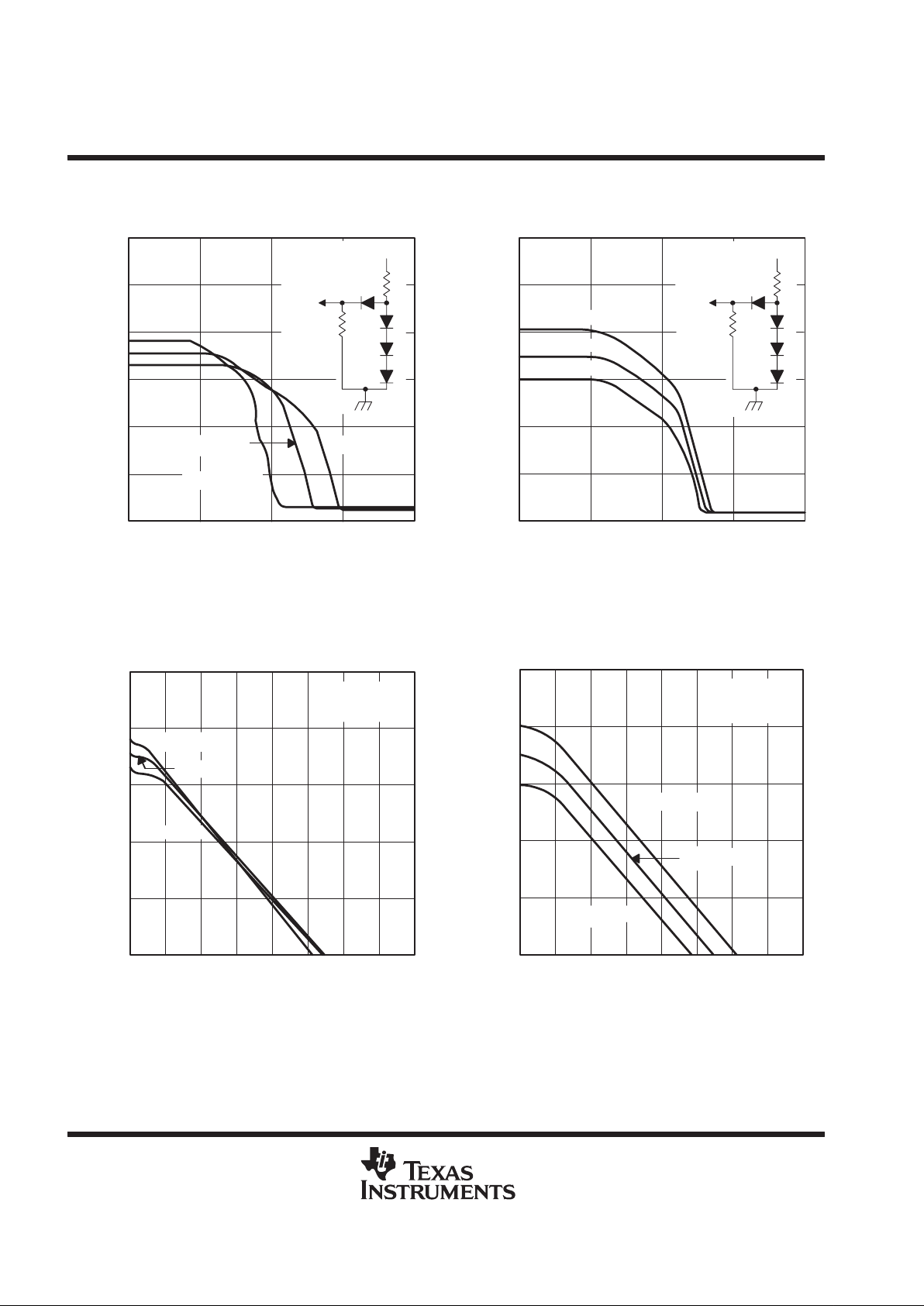
TYPICAL CHARACTERISTICS
†
Figure 3
V
I(S)
= 0.8 V
VCC = 5 V
5
4
3
2
1
321
0
4
6
V
I(D)
– Driver Input Voltage – V
VO(D) – Driver Output Voltage – V
0
DRIVER TRANSFER CHARACTERISTICS
V
O(D)
TA = 25°C
TA = –55°C
TA = 125°C
Figure 4
TA = 25°C
Load = 50 Ω to V
CC
V
I(S)
= 0.8 V
VCC = 4.5 V
VCC = 5 V
0
VO(D) – Driver Output Voltage – V
V
I(D)
– Driver Input Voltage – V
6
4
0
1 2 3
1
2
3
4
5
DRIVER TRANSFER CHARACTERISTICS
V
O(D)
VCC = 5.5 V
Figure 5
TA = 125°C
TA = 25°C
V
I(S)
– Strobe Input Voltage – V
5
4
3
2
1
321
0
4
6
VO(D) – Driver Output Voltage – V
0
STROBE-TO-DRIVER OUTPUT
TRANSFER CHARACTERISTICS
V
O(D)
TA = –55°C
Load = 50 Ω to V
CC
VCC = 5 V
V
I(D)
= 2 V
Figure 6
VCC = 4.5 V
VCC = 5.5 V
V
I(D)
= 2 V
STROBE-TO-DRIVER OUTPUT
TRANSFER CHARACTERISTICS
5
4
3
2
1
321
0
4
6
0
V
I(S)
– Strobe Input Voltage – V
VCC = 4.5 V
VCC = 5 V
VCC = 5.5 V
VO(D) – Driver Output Voltage – V
V
O(D)
Load = 50 Ω to V
CC
TA = 25°C
†
Data for temperatures below 0°C and above 70°C is applicable to SN55138 circuits only.
SN55138, SN75138
QUADRUPLE BUS TRANSCEIVERS
SLLS079B – SEPTEMBER 1973 – REVISED MA Y 1995
8
POST OFFICE BOX 655303 • DALLAS, TEXAS 75265
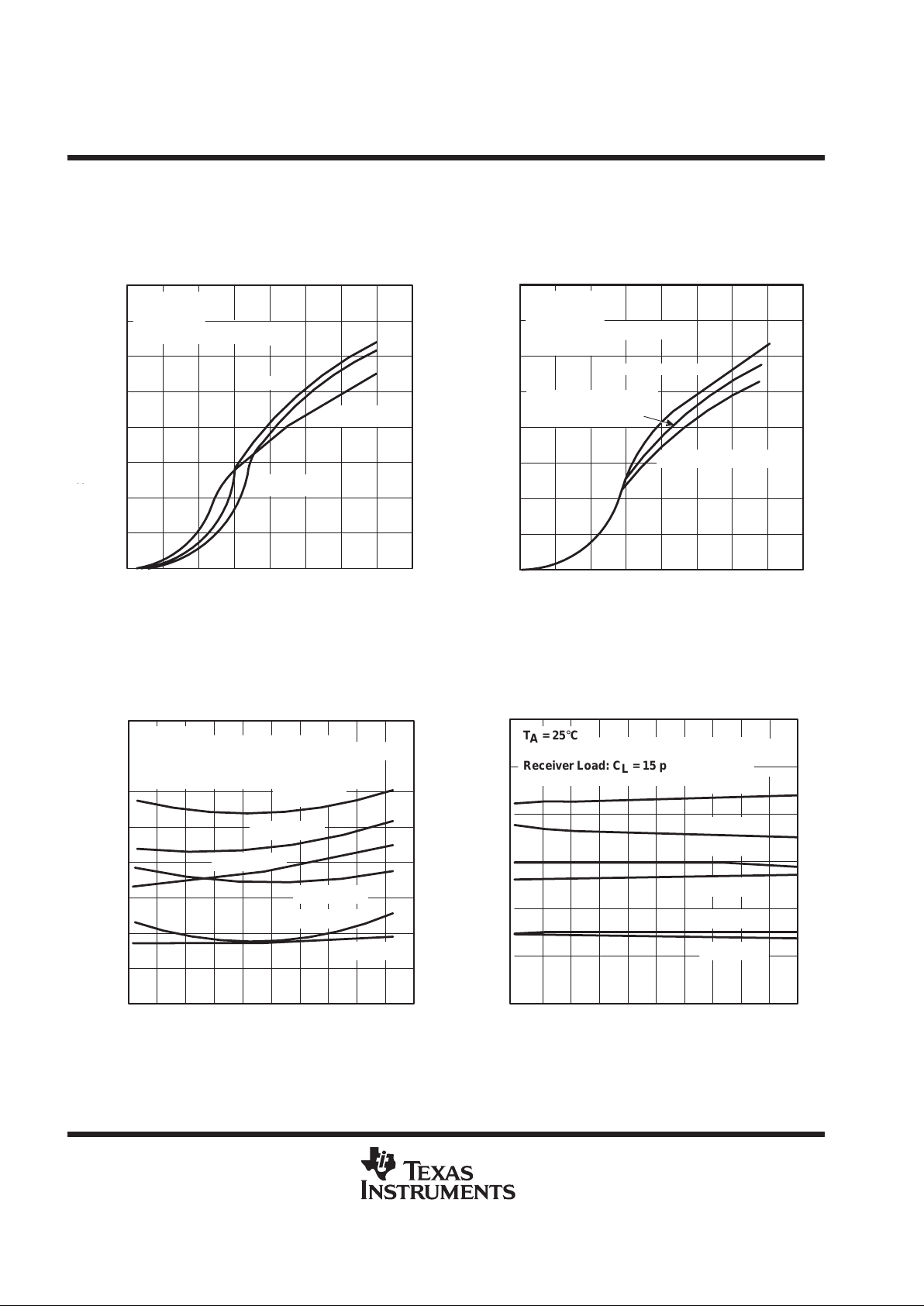
TYPICAL CHARACTERISTICS
†
Figure 7
VO(R) – Receiver Output Voltage – V
V
I(R)
– Receiver Input Voltage – V
RECEIVER TRANSFER CHARACTERISTICS
1N914
All Diodes
R
10 kΩ
400 Ω
5 V
Load:
VCC = 5 V
TA = 25°C
01234
6
0
1
2
3
4
5
V
O(R)
TA = – 55°C
TA = 125°C
Figure 8
R
10 kΩ
400 Ω
5 V
Load:
TA = 25°C
0
6
4
0
123
1
2
3
4
5
RECEIVER TRANSFER CHARACTERISTICS
VCC = 4.5 V
VCC = 5 V
VCC = 5.5 V
VO(R) – Receiver Output Voltage – V
V
O(R)
V
I(R)
– Receiver Input Voltage – V
1N914
All Diodes
Figure 9
TA = 25°C
VCC = 5 V
TA = – 55°C
TA = 125°C
4
3
2
1
3530252015105
0
40
5
I
OH(R)
– High-Level Output Current – mA
– High–Level Output Voltage – V
0
HIGH-LEVEL OUTPUT VOLTAGE
vs
HIGH-LEVEL OUTPUT CURRENT (RECEIVER)
V
OH
Figure 10
VCC = 5.5 V
VCC = 4.5 V
VCC = 5 V
V
I(R)
= 0.8 V
TA = 25°C
0405101520253035
HIGH-LEVEL OUTPUT VOLTAGE
vs
HIGH-LEVEL OUTPUT CURRENT (RECEIVER)
– High–Level Output Voltage – V
I
OH(R)
– High-Level Output Current – mA
4
3
2
1
0
5
V
OH
†
Data for temperatures below 0°C and above 70°C is applicable to SN55138 circuits only.

SN55138, SN75138
QUADRUPLE BUS TRANSCEIVERS
SLLS079B – SEPTEMBER 1973 – REVISED MA Y 1995
9
POST OFFICE BOX 655303 • DALLAS, TEXAS 75265
TYPICAL CHARACTERISTICS
†
Figure 11
VOL(R) – Low-Level Output Voltage – V
0.6
V
OL
1
0.8
0.4
0.2
5040302010
0
60
1.2
I
OL(R)
– Low-Level Output Current – mA
0
LOW-LEVEL OUTPUT VOLTAGE
vs
LOW-LEVEL OUTPUT CURRENT (RECEIVER)
TA = 125°C
TA = 25°C
VCC = 4.5 V
V
I(R)
= 3.5 V
TA = – 55°C
Figure 12
TA = 25°C
V
I(S)
= 0.8 V
0
1.2
300
0
50 100 150 200 250
0.2
0.4
0.6
0.8
1
LOW-LEVEL OUTPUT VOLTAGE
vs
LOW-LEVEL OUTPUT CURRENT (DRIVER)
I
OL(D)
– Low-Level Output Current – mA
TA = 125°C
VCC = 4.5 V
V
I(D)
= 2 V
VOL(R) – Low-Level Output Voltage – VV
OL
TA = – 55°C
Figure 13
V
I(R)
– Receiver Input Voltage – V
VCC = 5 V
TA = 25°C, – 55°C
TA = 125°C
1.4
1.2
1
0.8
0.6
0.4
0.2
54321
0
6
1.6
II(R) – Receiver Input Current – mA
0
RECEIVER INPUT CURRENT
vs
RECEIVER INPUT VOLTAGE
I
I(R)
V
I(S)
= 2 V
TA = 125°C, 25°C
TA = – 55°C
Figure 14
V
I(R)
– Receiver Input Voltage – V
RECEIVER INPUT CURRENT
vs
RECEIVER INPUT VOLTAGE
0
1.6
6
0
1 2345
0.2
0.4
0.6
0.8
1
1.2
1.4
V
I(S)
= 2 V
II(R) – Receiver Input Current – mA
I
I(R)
TA = 25°C
VCC = 4.5 V
VCC = 5 V
VCC = 5.5 V
†
Data for temperatures below 0°C and above 70°C is applicable to SN55138 circuits only.
SN55138, SN75138
QUADRUPLE BUS TRANSCEIVERS
SLLS079B – SEPTEMBER 1973 – REVISED MA Y 1995
10
POST OFFICE BOX 655303 • DALLAS, TEXAS 75265
TYPICAL CHARACTERISTICS
†
Figure 15
Driver Loads = 1 kΩ to 5 V
V
I(D)
= 2 V
V
I(S)
= 0.8 V
TA = – 55°C
70
60
50
40
30
20
10
7654321
0
8
80
VCC – Supply Voltage – V
ICC – Supply Current – mA
0
SUPPLY CURRENT
vs
SUPPLY VOLTAGE
(ALL DRIVER OUTPUTS LOW)
CC
I
TA = 125°C
TA = 25°C
Figure 16
VCC – Supply Voltage – V
ICC – Supply Current – mA
SUPPLY CURRENT
vs
SUPPLY VOLTAGE
R Output Open
0
80
8
0
1 2 3 4 67
10
20
30
40
50
60
70
TA = 25°C
V
I(S)
= 0.8 V
Driver Loads = 1 kΩ to 5 V
5
4 Driver Inputs at 0.8 V
4 Driver Inputs at 2 V
CC
I
2 Driver Inputs at 2 V,
2 Driver Inputs at 0.8 V
Figure 17
Propagation Delay Times – ns
t
PLH
(D-D)
Driver Load: CL = 50 pF, RL = 50 Ω, See Figure 1
VCC = 5 V
28
24
20
16
12
8
4
120100806040200–20–40
0
140
32
TA – Free-Air Temperature – °C
–6
PROPAGATION DELAY TIMES
vs
FREE-AIR TEMPERATURE
t
PLH
(S-D)
Receiver Load: CL = 15 pF, RL = 400 Ω,
See Figure 2
t
PHL
(S-D)
t
PHL
(D-D)
t
PLH
(R-R)
t
PHL
(R-R)
Figure 18
Propagation Delay Times – ns
t
PLH(R-R)
t
PHL(R-R)
t
PHL(D-D)
t
PLH(D-D)
t
PLH(S-D)
40
20
15
10
5
5.45.35.25.154.94.84.74.6
0
5.5
30
4.5
VCC – Supply Voltage – V
PROPAGATION DELAY TIMES
vs
SUPPLY VOLTAGE
TA = 25°C
Receiver Load: CL = 15 pF, RL = 400 Ω,
See Figure 2
Driver Load: CL = 50 pF, RL = 50 Ω, See Figure 1
t
PHL(S-D)
†
Data for temperatures below 0°C and above 70°C is applicable to SN55138 circuits only.

SN55138, SN75138
QUADRUPLE BUS TRANSCEIVERS
SLLS079B – SEPTEMBER 1973 – REVISED MA Y 1995
11
POST OFFICE BOX 655303 • DALLAS, TEXAS 75265
TYPICAL CHARACTERISTICS
Figure 19
15
10
5
0
0 20 40 60 80 100 120
20
25
DRIVER
PROPAGATION DELAY TIMES
vs
LOAD CAPACITANCE
30
140 160 180 200
– Propagation Delay Times – ns
CL – Load Capacitance – pF
t
PHL(S-D)
t
PLH(S-D)
t
PHL(D-D)
t
PLH(D-D)
VCC = 5 V
RL = 50 W,
See Figure 1
TA = 25_C
t
pd
Figure 20
8
4
2
0
01020304050
– Propagation Delay Times – ns
12
14
RECEIVER
PROPAGATION DELAY TIMES
vs
LOAD CAPACITANCE
16
60 70 80
10
6
t
PHL(R-R)
t
PLH(R-R)
VCC = 5 V
RL = 400 Ω, See Figure 2
TA = 25°C
CL – Load Capacitance – pF
t
pd
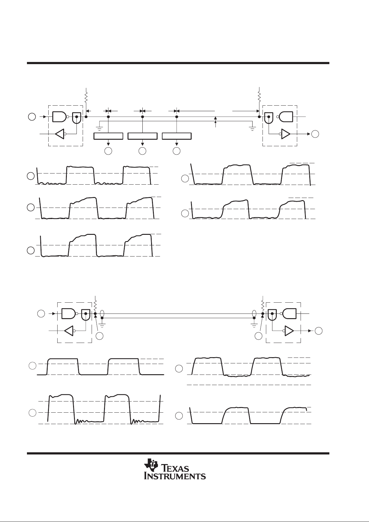
APPLICATION INFORMATION
B
1/4 SN55138
A
5 V
100 Ω
5 V
100 Ω
1/4 SN55138
C
D
P
50 ft Belden #8795
100-Ω Telephone Cable
3 V
2 V
0 V
5 V
4 V
2 V
0 V
5 V
4 V
2 V
0 V
4 V
2 V
0 V
TYPICAL VOLTAGE WAVEFORMS
A
B
C
D
Figure 21. Point-to-Point Communication Over 50 Feet of Twisted Pair at 5 MHz
SN55138, SN75138
QUADRUPLE BUS TRANSCEIVERS
SLLS079B – SEPTEMBER 1973 – REVISED MA Y 1995
12
POST OFFICE BOX 655303 • DALLAS, TEXAS 75265
APPLICATION INFORMATION
0 V
4 V
2 V
4 V
2 V
0 V
0 V
2 V
4 V
0 V
2 V
4 V
0 V
2 V
3 V
E
D
C
B
A
P
250 ft100 ft100 ft
or Equivalent
Belden #8795
Telephone Cable
D
1/4 SN551381/4 SN551381/4 SN55138
CB
E
1/4 SN55138
100 Ω
5 V
100 Ω
5 V
A
1/4 SN55138
TYPICAL VOLTAGE WAVEFORMS
50 ft
Figure 22. Party-Line Communication on 500 Feet of Twisted Pair at 1 MHz
0 V
2 V
3 V
0 V
2 V
4 V
5 V
0 V
2 V
4 V
0 V
2 V
3 V
C
D
B
A
C
or Equivalent
1000 ft RG-53
B
5 V
100 Ω
1/4 SN55138
D
5 V
1/4 SN55138
A
100 Ω
TYPICAL VOLTAGE WAVEFORMS
5 V
Figure 23. Point-to-Point Communication Over 1000 Feet of Coaxial Cable at 1 MHz

IMPORTANT NOTICE
T exas Instruments and its subsidiaries (TI) reserve the right to make changes to their products or to discontinue
any product or service without notice, and advise customers to obtain the latest version of relevant information
to verify, before placing orders, that information being relied on is current and complete. All products are sold
subject to the terms and conditions of sale supplied at the time of order acknowledgement, including those
pertaining to warranty, patent infringement, and limitation of liability.
TI warrants performance of its semiconductor products to the specifications applicable at the time of sale in
accordance with TI’s standard warranty. Testing and other quality control techniques are utilized to the extent
TI deems necessary to support this warranty. Specific testing of all parameters of each device is not necessarily
performed, except those mandated by government requirements.
CERT AIN APPLICATIONS USING SEMICONDUCTOR PRODUCTS MAY INVOL VE POTENTIAL RISKS OF
DEATH, PERSONAL INJURY, OR SEVERE PROPERTY OR ENVIRONMENTAL DAMAGE (“CRITICAL
APPLICATIONS”). TI SEMICONDUCTOR PRODUCTS ARE NOT DESIGNED, AUTHORIZED, OR
WARRANTED TO BE SUITABLE FOR USE IN LIFE-SUPPORT DEVICES OR SYSTEMS OR OTHER
CRITICAL APPLICATIONS. INCLUSION OF TI PRODUCTS IN SUCH APPLICA TIONS IS UNDERST OOD TO
BE FULLY AT THE CUSTOMER’S RISK.
In order to minimize risks associated with the customer’s applications, adequate design and operating
safeguards must be provided by the customer to minimize inherent or procedural hazards.
TI assumes no liability for applications assistance or customer product design. TI does not warrant or represent
that any license, either express or implied, is granted under any patent right, copyright, mask work right, or other
intellectual property right of TI covering or relating to any combination, machine, or process in which such
semiconductor products or services might be or are used. TI’s publication of information regarding any third
party’s products or services does not constitute TI’s approval, warranty or endorsement thereof.
Copyright 1998, Texas Instruments Incorporated
 Loading...