

SN75124
TRIPLE LINE RECEIVER
SLLS058B – SEPTEMBER 1973 – REVISED MA Y 1995
1
POST OFFICE BOX 655303 • DALLAS, TEXAS 75265
D
Meets or Exceeds the Requirements of
IBM System 360 Input/Output Interface
Specification
D
Operates From Single 5-V Supply
D
TTL Compatible
D
Built-In Input Threshold Hysteresis
D
High Speed . . . Typical Propagation Delay
Time = 20 ns
D
Independent Channel Strobes
D
Input Gating Increases Application
Flexibility
D
Designed for Use With Dual Line Driver
SN75123
D
Designed to Be Interchangeable With
Signetics N8T24
description
The SN75124 triple line receiver is specifically designed to meet the input/output interface specifications for IBM
System 360. It is also compatible with standard TTL logic and supply voltage levels.
The SN75124 has receiver inputs with built-in hysteresis to provide increased noise margin for single-ended
systems. An open line affects the receiver input as does a low-level input voltage, and the receiver input can
withstand a level of –0.15 V with power on or off. The other inputs are in TTL configuration. The S input must
be high to enable the receiver input. Two of the line receivers have A and B inputs that, if both are high, hold
the output low. The third receiver has only an A input that, if high, holds the output low.
See the SN751730 for new IBM 360/370 interface designs.
The SN75124 is characterized for operation from 0°C to 70°C.
FUNCTION TABLE
INPUTS
OUTPUT
A
B
†
R S
OUTPUT
Y
H H X X L
X XLH L
LXHX H
LXXL H
XLHX H
XLXL H
†
B input and last two lines of the function table are
applicable to receivers 1 and 2 only.
Copyright 1995, Texas Instruments Incorporated
PRODUCTION DATA information is current as of publication date.
Products conform to specifications per the terms of Texas Instruments
standard warranty. Production processing does not necessarily include
testing of all parameters.
Please be aware that an important notice concerning availability, standard warranty, and use in critical applications of
Texas Instruments semiconductor products and disclaimers thereto appears at the end of this data sheet.
1
2
3
4
5
6
7
8
16
15
14
13
12
11
10
9
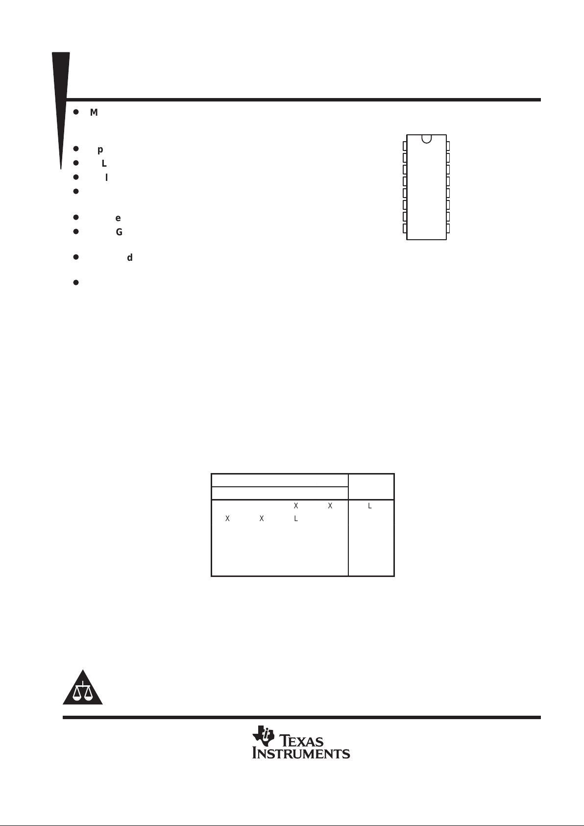
1A
1B
2R
2S
2A
2B
2Y
GND
V
CC
1S
1R
1Y
3A
3S
3R
3Y
D OR N PACKAGE
(TOP VIEW)
IBM is a trademark of International Business Machines Corp.
SN75124
TRIPLE LINE RECEIVER
SLLS058B – SEPTEMBER 1973 – REVISED MA Y 1995
2
POST OFFICE BOX 655303 • DALLAS, TEXAS 75265
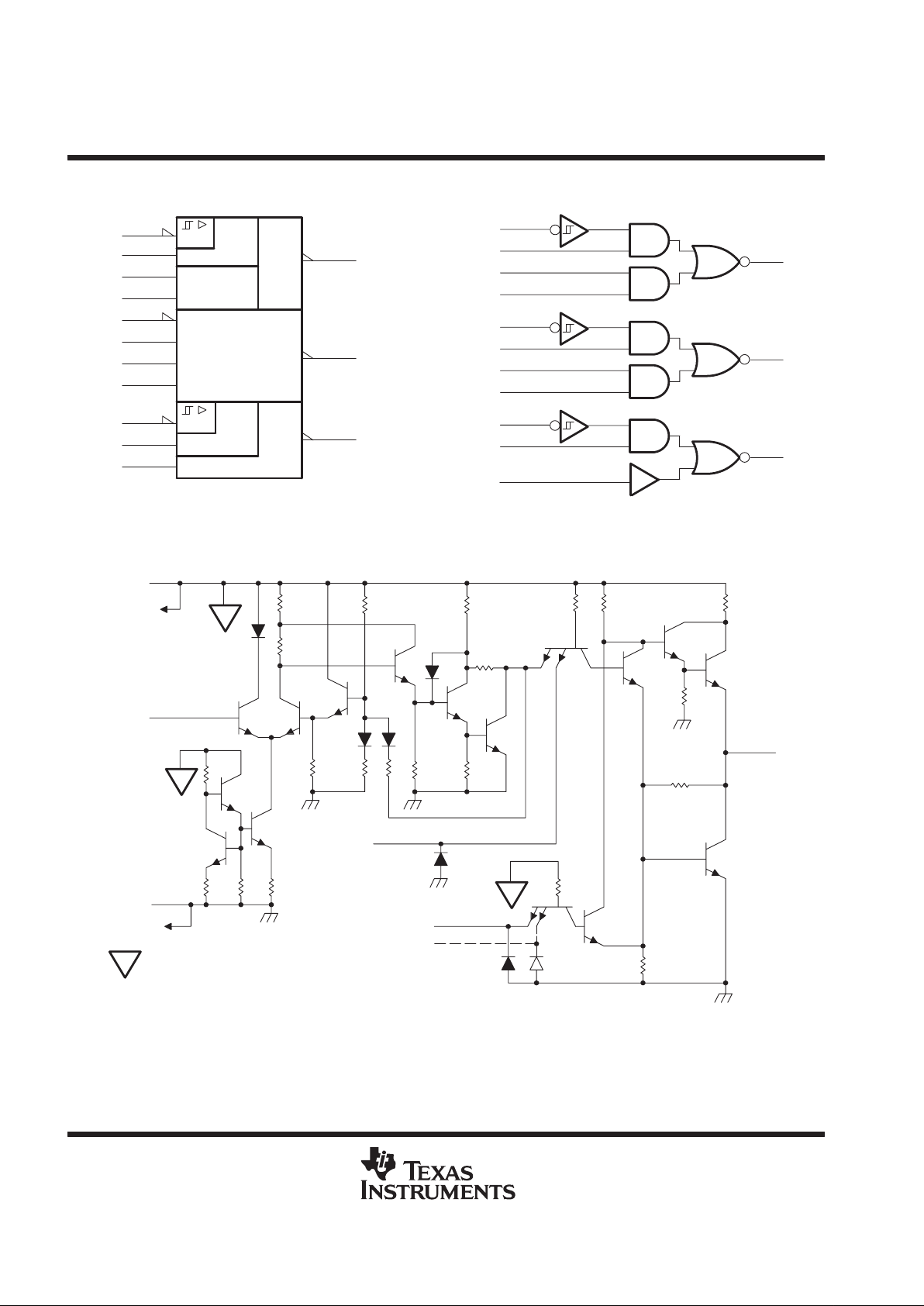
logic symbol
†
2Y
15
12
11
10
6
5
4
3
2
1
14
3Y
1Y
9
7
13
3A
3S
3R
2B
2A
2S
2R
1B
1A
1S
1R
≥ 1
&
&
&
†
This symbol is in accordance with ANSI/IEEE Std 91-1984
and IEC Publication 617-12.
≥ 1
logic diagram (positive logic)
3A
3S
3R
2B
2A
2S
2R
1B
1A
1S
1R
9
7
13
1Y
2Y
3Y
12
11
10
6
5
4
3
2
1
15
14
schematic (each receiver)
58 Ω
13, 7, 9
Y
800 Ω4 kΩ
4 kΩ
A
B
‡
1, 5, 12
2, 6
S
15, 4, 11
16
V
CC
14, 3, 10
R
8
GND
...VCC bus
To Other
Receivers
V
V
V
V
To Other
Receivers
‡
B input is provided on receivers 1 and 2 only
Resistor values shown are nominal.

SN75124
TRIPLE LINE RECEIVER
SLLS058B – SEPTEMBER 1973 – REVISED MA Y 1995
3
POST OFFICE BOX 655303 • DALLAS, TEXAS 75265
absolute maximum ratings over operating free-air temperature range (unless otherwise noted)
†
Supply voltage, V
CC
(see Note 1) 7 V. . . . . . . . . . . . . . . . . . . . . . . . . . . . . . . . . . . . . . . . . . . . . . . . . . . . . . . . . . . . .
Input voltage, V
I
: R input with VCC applied 7 V. . . . . . . . . . . . . . . . . . . . . . . . . . . . . . . . . . . . . . . . . . . . . . . . . . .
R input with V
CC
not applied 6 V. . . . . . . . . . . . . . . . . . . . . . . . . . . . . . . . . . . . . . . . . . . . . . . .
A, B, or S input 5.5 V. . . . . . . . . . . . . . . . . . . . . . . . . . . . . . . . . . . . . . . . . . . . . . . . . . . . . . . . . .
Output voltage, V
O
7 V. . . . . . . . . . . . . . . . . . . . . . . . . . . . . . . . . . . . . . . . . . . . . . . . . . . . . . . . . . . . . . . . . . . . . . . . .
Output current, I
O
±100 mA. . . . . . . . . . . . . . . . . . . . . . . . . . . . . . . . . . . . . . . . . . . . . . . . . . . . . . . . . . . . . . . . . . . . . .
Continuous total dissipation See Dissipation Rating Table. . . . . . . . . . . . . . . . . . . . . . . . . . . . . . . . . . . . . . . . . . .
Operating free-air temperature range, T
A
0°C to 70°C. . . . . . . . . . . . . . . . . . . . . . . . . . . . . . . . . . . . . . . . . . . . . .
Storage temperature range, T
stg
–65°C to 150°C. . . . . . . . . . . . . . . . . . . . . . . . . . . . . . . . . . . . . . . . . . . . . . . . . . .
Lead temperature 1,6 mm (1/16 inch) from case for 10 seconds 260°C. . . . . . . . . . . . . . . . . . . . . . . . . . . . . . .
†
Stresses beyond those listed under “absolute maximum ratings” may cause permanent damage to the device. These are stress ratings only, and
functional operation of the device at these or any other conditions beyond those indicated under “recommended operating conditions” is not
implied. Exposure to absolute-maximum-rated conditions for extended periods may affect device reliability.
NOTE 1: Voltage values are with respect to network ground terminal
DISSIPATION RATING TABLE
TA ≤ 25°C DERATING FACTOR TA = 70°C
PACKAGE
A
POWER RATING ABOVE TA = 25°CAPOWER RATING
D 950 mW 7.6 mW/°C 608 mW
N 1150 mW 9.2 mW/°C 736 mW
recommended operating conditions
MIN NOM MAX UNIT
Supply voltage, V
CC
4.75 5 5.25 V
p
A, B, or S 2
High-level input voltage, V
IH
R 1.7
V
p
A, B, or S 0.8
Low-level input voltage, V
IL
R 0.7
V
High-level output current, I
OH
–800 µA
Low-level output current, I
OL
16 mA
Operating free-air temperature, T
A
0 70 °C

SN75124
TRIPLE LINE RECEIVER
SLLS058B – SEPTEMBER 1973 – REVISED MA Y 1995
4
POST OFFICE BOX 655303 • DALLAS, TEXAS 75265
electrical characteristics over recommended ranges of supply voltage and operating free-air
temperature (unless otherwise noted)
PARAMETER TEST CONDITIONS MIN TYP MAX UNIT
V
hys
Hysteresis voltage (V
IT+
– V
IT–
) R VCC = 5 V, TA = 25°C 0.2 0.5 V
V
IK
Input clamp voltage A, B, or S VCC = 5 V, II –12 mA –1.5 V
V
I(BR)
Input breakdown voltage A, B, or S VCC = 5 V, II = 10 mA 5.5 V
p
V
= V
min, V
= V
max,
VOHHigh-level output voltage
IH IH
,
IOH = –800 µA,
IL IL
,
See Note 2
2.6
V
p
V
= V
min, V
= V
max,
VOLLow-level output voltage
IH IH
,
IOL = 16 mA,
IL IL
,
See Note 2
0.4
V
p
p
VI = 7 V 5
IIInput current at maximum input voltage
R
VI = 6 V, VCC = 0 5
mA
p
A, B, or S VI = 4.5 V 40
IIHHigh-level input current
R VI = 3.11 V 170
µ
A
I
IL
Low-level input current A, B, or S VI = 0.4 V, VIR = 0.8 V –0.1 –1.6 mA
I
OS
Short-circuit output current
†
–50 –100 mA
pp
All inputs = 0.8 V 72
ICCSupply current
All inputs = 2 V 100
mA
†
Not more than one output should be shorted at a time, and duration of the short circuit should not exceed one second.
NOTE 2: The output voltage and current limits are characterized for any appropriate combination of high and low inputs specified by the function
table for the desired output.
switching characteristics, VCC = 5 V, TA = 25°C
PARAMETER TEST CONDITIONS MIN TYP MAX UNIT
t
PLH
Propagation delay time, low-to-high-level output from R input
20 30
t
PHL
Propagation delay time, high-to-low-level output from R input
See Figure 1
20 30
ns
PARAMETER MEASUREMENT INFORMATION
V
CC
2.6 V
84.5 Ω
1N3064
Output
5 kΩ
CL =
30 pF
See Note B
TEST CIRCUIT
Pulse
Generator
(see Note A)
≤ 5 ns
90%
1.5 V
Input
10%
0
2.6 V
V
OH
Output
V
OL
t
PHL
t
PLH
VOLTAGE WAVEFORMS
≤ 5 ns
90%
1.5 V
10%
1.5 V 1.5 V
NOTES: A. The pulse generator has the following characteristics: ZO ≈ 50 Ω, PRR ≤ 5 MHz, duty cycle = 50%.
B. CL includes probe and jig capacitance.
Figure 1. Test Circuit and Voltage Waveforms

SN75124
TRIPLE LINE RECEIVER
SLLS058B – SEPTEMBER 1973 – REVISED MA Y 1995
5
POST OFFICE BOX 655303 • DALLAS, TEXAS 75265
TYPICAL CHARACTERISTICS
VO – Output Voltage – V
V
O
VI – Input Voltage – V
VCC = 5 V
No Load
TA = 25°C
RECEIVER
OUTPUT VOLTAGE
vs
INPUT VOLTAGE
0
4
2
0
0.4 0.8 1 1.4 1.8
0.5
1
1.5
2
2.5
3
3.5
V
IT–
V
IT+
0.2 0.6 1.2 1.6
Figure 2
APPLICATION INFORMATION
1/2 SN75123
95 Ω
95-Ω Coaxial Cable
A
B
C
D
E
F
95 Ω
Strobe
A
B
Y
1/3 SN75124
Figure 3. Unbalanced Line Communication Using SN75123 and SN75124

IMPORTANT NOTICE
T exas Instruments and its subsidiaries (TI) reserve the right to make changes to their products or to discontinue
any product or service without notice, and advise customers to obtain the latest version of relevant information
to verify, before placing orders, that information being relied on is current and complete. All products are sold
subject to the terms and conditions of sale supplied at the time of order acknowledgement, including those
pertaining to warranty, patent infringement, and limitation of liability.
TI warrants performance of its semiconductor products to the specifications applicable at the time of sale in
accordance with TI’s standard warranty. Testing and other quality control techniques are utilized to the extent
TI deems necessary to support this warranty. Specific testing of all parameters of each device is not necessarily
performed, except those mandated by government requirements.
CERT AIN APPLICATIONS USING SEMICONDUCTOR PRODUCTS MAY INVOLVE POTENTIAL RISKS OF
DEATH, PERSONAL INJURY, OR SEVERE PROPERTY OR ENVIRONMENTAL DAMAGE (“CRITICAL
APPLICATIONS”). TI SEMICONDUCTOR PRODUCTS ARE NOT DESIGNED, AUTHORIZED, OR
WARRANTED TO BE SUITABLE FOR USE IN LIFE-SUPPORT DEVICES OR SYSTEMS OR OTHER
CRITICAL APPLICATIONS. INCLUSION OF TI PRODUCTS IN SUCH APPLICA TIONS IS UNDERST OOD TO
BE FULLY AT THE CUSTOMER’S RISK.
In order to minimize risks associated with the customer’s applications, adequate design and operating
safeguards must be provided by the customer to minimize inherent or procedural hazards.
TI assumes no liability for applications assistance or customer product design. TI does not warrant or represent
that any license, either express or implied, is granted under any patent right, copyright, mask work right, or other
intellectual property right of TI covering or relating to any combination, machine, or process in which such
semiconductor products or services might be or are used. TI’s publication of information regarding any third
party’s products or services does not constitute TI’s approval, warranty or endorsement thereof.
Copyright 1998, Texas Instruments Incorporated
 Loading...