


SN55116, SN75116, SN75117, SN75118, SN75119
DIFFERENTIAL LINE TRANSCEIVERS
SLLS073D – MAY 1976 – REVISED MAY 1998
1
POST OFFICE BOX 655303 • DALLAS, TEXAS 75265
features common to all types
D
Single 5-V Supply
D
3-State Driver Output Circuitry
D
TTL-Compatible Driver Inputs
D
TTL-Compatible Receiver Output
D
Differential Line Operation
D
Receiver Output Strobe (SN55116,
SN75116, SN75117) or Enable (SN75118,
SN75119)
D
Designed for Party-Line (Data-Bus)
Applications
additional features of the SN55116/SN75116
D
Choice of Ceramic or Plastic Packages
D
Independent Driver and Receiver
D
Choice of Open-Collector or Totem-Pole
Outputs on Both Driver and Receiver
D
Dual Data Inputs on Driver
D
Optional Line-Termination Resistor in
Receiver
D
±15-V Receiver Common-Mode Capability
D
Receiver Frequency-Response Control
additional features of the SN75117
D
Driver Output Internally Connected to
Receiver Input
The SN75118 is an SN75116 With 3-State Receiver Output Circuitry
The SN75119 is an SN75117 With 3-State Receiver Output Circuitry
description
These integrated circuits are designed for use in interfacing between TTL-type digital systems and differential
data-transmission lines. They are especially useful for party-line (data-bus) applications. Each of these circuit
types combine in one package a 3-state differential line driver and a differential-input line receiver , both of which
operate from a single 5-V power supply. The driver inputs and the receiver outputs are TTL compatible. The
driver employed is similar to the SN55113 and SN75113 3-state line drivers, and the receiver is similar to the
SN55115 and SN75115 line receivers.
The SN55116, SN75116, and SN75118 offer all the features of the SN55113 and SN75113 drivers and the
SN551 15 and SN75115 receivers combined. The driver performs the dual input AND and NAND functions when
enabled or presents a high impedance to the load when in the disabled state. The driver output stages are similar
to TTL totem-pole outputs, but have the current-sinking portion separated from the current-sourcing portion and
both are brought out to adjacent package terminals. This feature allows the user the option of using the driver
in the open-collector output configuration, or, by connecting the adjacent source and sink terminals together,
of using the driver in the normal totem-pole output configuration.
The receiver portion of the SN55116, SN75116, and SN75118 features a differential-input circuit having a
common-mode voltage range of ±15 V . An internal 130-Ω equivalent resistor also is provided, which optionally
can be used to terminate the transmission line. A frequency-response control terminal allows the user to reduce
the speed of the receiver or to improve differential noise immunity . The receivers of the SN551 16 and SN751 16
have an output strobe and a split totem-pole output. The receiver of the SN751 18 has an output-enable for the
3-state split totem-pole output. The receiver section of either circuit is independent of the driver section except
for the V
CC
and ground terminals.
The SN75117 and SN75119 provide the basic driver and receiver functions of the SN55116, SN75116, and
SN75118, but use a package that is only half as large. The SN75117 and SN75119 are intended primarily for
party-line or bus-organized systems because the driver outputs are internally connected to the receiver inputs.
The driver has a single data input and a single enable input. The SN751 17 receiver has an output strobe, while
the SN751 19 receiver has a 3-state output enable. However, these devices do not provide output connection
options, line-termination resistors, or receiver frequency-response controls.
Copyright 1998, Texas Instruments Incorporated
PRODUCTION DATA information is current as of publication date.
Products conform to specifications per the terms of Texas Instruments
standard warranty. Production processing does not necessarily include
testing of all parameters.
Please be aware that an important notice concerning availability, standard warranty, and use in critical applications of
Texas Instruments semiconductor products and disclaimers thereto appears at the end of this data sheet.
SN55116, SN75116, SN75117, SN75118, SN75119
DIFFERENTIAL LINE TRANSCEIVERS
SLLS073D – MAY 1976 – REVISED MAY 1998
2
POST OFFICE BOX 655303 • DALLAS, TEXAS 75265
description (continued)
The SN55116 is characterized for operation over the full military temperature range of –55°C to 125°C. The
SN75116, SN75117, SN75118, and SN75119 are characterized for operation from 0°C to 70°C.
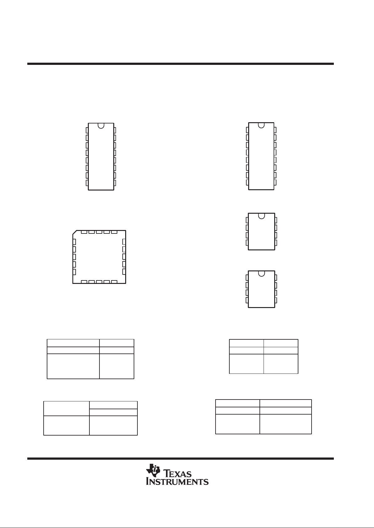
1
2
3
4
5
6
7
8
16
15
14
13
12
11
10
9
DZP
DZS
DYS
DYP
RA
R
T
RB
GND
V
CC
DB
DA
DE
RYP
RYS
RS
RTC
SN55116 ...J PACKAGE
SN75116 ...D OR N PACKAGE
(TOP VIEW)
1
2
3
4
5
6
7
8
16
15
14
13
12
11
10
9
DZP
DZS
DYS
DYP
RA
R
T
RB
GND
V
CC
DB
DA
DE
RYP
RYS
RE
RTC
SN75118 ...D OR N PACKAGE
(TOP VIEW)
3 2 1 20 19
910111213
4
5
6
7
8
18
17
16
15
14
DA
DE
NC
RYP
RYS
DYS
DYP
NC
RA
R
T
SN55116 . . . FK PACKAGE
(TOP VIEW)
DZS
DZP
NCRSDB
RB
GND
NC
NC – No internal connection
CC
V
RTC
1
2
3
4
8
7
6
5
DI
B
A
GND
V
CC
DE
RY
RS
SN75117 ...D OR P PACKAGE
(TOP VIEW)
1
2
3
4
8
7
6
5
DI
B
A
GND
V
CC
DE
RY
RE
SN75119 ...D OR P PACKAGE
(TOP VIEW)
Function Tables
INPUTS
OUTPUTS
L
H
H
H
’116, SN75118
DRIVER
DE DA DB
X
L
X
H
X
X
L
H
DY DZ
Z
L
L
H
Z
H
H
L
INPUTS
OUTPUTS
SN75117, SN75119
DRIVER
DI DE
H
L
X
H
H
L
AB
H
L
Z
L
H
Z
OUTPUTS RY
’116, SN75118
RECEIVER
RS/RE
DIFF
INPUT
L
H
H
X
L
H
’116 SN75118
H
H
L
Z
H
L
INPUTS
OUTPUT RY
SN75117, SN75119
RECEIVER
B RS/RE
L
H
X
H
H
L
SN75117 SN75119
H
L
H
H
L
Z
A
H
L
X
H = high level (VI ≥ VIH min or VID more positive than VTH max), L = low level (VI ≤ VIL max or VID more negative than VTL max),
X = irrelevant, Z = high impedance (off)

SN55116, SN75116, SN75117, SN75118, SN75119
DIFFERENTIAL LINE TRANSCEIVERS
SLLS073D – MAY 1976 – REVISED MAY 1998
3
POST OFFICE BOX 655303 • DALLAS, TEXAS 75265
logic symbol
†
EN
B
A
6
5
1
7
RY
RS
DI
DE
2
3
&
&
&
RESP
R
T
EN
9
10
6
5
7
15
14
13
RYS
RYP
DZS
DZP
DYS
DYP
RTC
RS
R
T
RA
RB
DB
DA
DE
11
12
2
1
3
4
’116
‡
&
RESP
R
T
EN
9
10
6
5
7
15
14
13
RYS
RYP
DZS
DZP
DYS
DYP
RTC
RE
R
T
RA
RB
DB
DA
DE
11
12
2
1
3
4
SN75118
‡
EN
SN75117
‡
EN
B
A
6
5
1
7
RY
RE
DI
DE
2
3
SN75119
‡
EN
5
ogic diagram (positive logic)
6
3
2
5
7
1
RE
DE
DI RY
A
B
BUS
BUS
B
A
RY
DI
DE
RS
1
7
5
2
3
6
RTC
R
T
RA
RB
RE
9
6
5
7
10
RYP (pullup)
RYS (sink)
12
11
RS
RTC
R
T
RA
RB
10
9
6
7
RYS (sink)
RYP (pullup)
11
12
DB
DA
DE
15
14
13
DZS (sink)
DZP (pullup)
DYS (sink)
DYP (pullup)
2
1
3
4
’116 and SN75118
‡
’116 Receiver
‡
SN75118 Receiver
‡
SN75119 Driver and Receiver
‡
SN75117 Driver and Receiver
‡
†
These symbols are in accordance with ANSI/IEEE Std 91-1984 and IEC Publication 617-12.
‡
Pin numbers shown for the SN55116 and SN751 16 are for the D, J, and N packages, those shown for the SN751 18 are for the D and N packages,
and those shown for SN75117 and SN75119 are for the D and P packages.
SN55116, SN75116, SN75117, SN75118, SN75119
DIFFERENTIAL LINE TRANSCEIVERS
SLLS073D – MAY 1976 – REVISED MAY 1998
4
POST OFFICE BOX 655303 • DALLAS, TEXAS 75265
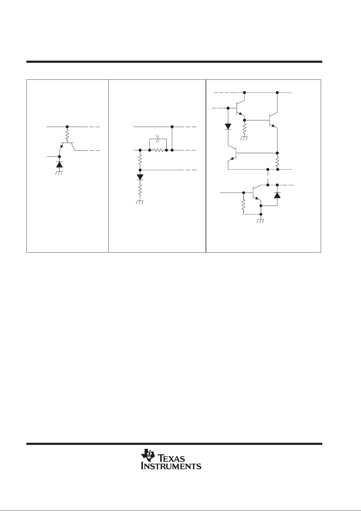
schematics of inputs and outputs
7 kΩ
NOM
EQUIVALENT OF
EACH DRIVER INPUT
AND EACH RE AND RS INPUT
V
CC
Input
4 kΩ
NOM
EQUIVALENT OF
EACH RECEIVER INPUT
(EXCLUDING ENABLES AND STROBES)
V
CC
1 pF NOM
Input
8 kΩ
NOM
130 Ω
NOM
TYPICAL OF ALL OUTPUTS
V
CC
R
Pullup
output
†
Driver output R = 9 Ω NOM
Receiver output R = 20 Ω NOM
Sink
output
†
†
On SN75117 and SN75119, common outputs
replace the separate pullup and sink outputs.
absolute maximum ratings over operating free-air temperature (unless otherwise noted)
‡
Supply voltage, V
CC
(see Notes 1 and 2) 7 V. . . . . . . . . . . . . . . . . . . . . . . . . . . . . . . . . . . . . . . . . . . . . . . . . . . . . .
Input voltage, V
I
: DA, DB, DE, DI, RE, and RS 5.5 V. . . . . . . . . . . . . . . . . . . . . . . . . . . . . . . . . . . . . . . . . . . . . . . .
RA, RB, R
T
for ’116, SN75118 only ±25 V. . . . . . . . . . . . . . . . . . . . . . . . . . . . . . . . . . . . . . . . . .
A and B for SN75117, SN75119 only 0 to 6 V. . . . . . . . . . . . . . . . . . . . . . . . . . . . . . . . . . . . . . .
Off-state voltage applied to open-collector outputs: ’116, SN75118 only 12 V. . . . . . . . . . . . . . . . . . . . . . . . . . .
Continuous total power dissipation (see Note 2) See Dissipation Rating Table. . . . . . . . . . . . . . . . . . . . . . . . . .
Storage temperature range, T
stg
–65°C to 150°C. . . . . . . . . . . . . . . . . . . . . . . . . . . . . . . . . . . . . . . . . . . . . . . . . . .
Case temperature for 60 seconds, T
C
: FK package 260°C. . . . . . . . . . . . . . . . . . . . . . . . . . . . . . . . . . . . . . . . . .
Lead temperature 1,6 mm (1/16 inch) from case for 60 seconds: J package 300°C. . . . . . . . . . . . . . . . . . . . .
Lead temperature 1,6 mm (1/16 inch) from case for 10 seconds: D, N, or P package 260°C. . . . . . . . . . . . .
‡
Stresses beyond those listed under “absolute maximum ratings” may cause permanent damage to the device. These are stress ratings only, and
functional operation of the device at these or any other conditions beyond those indicated under “recommended operating conditions” is not
implied. Exposure to absolute-maximum-rated conditions for extended periods may affect device reliability.
NOTES: 1. All voltage values are with respect to the network ground terminal.
2. In the FK and J packages, the SN55116 chip is alloy mounted. The SN75116, SN75117, SN75118, and SN75119 chips are glass
mounted.
SN55116, SN75116, SN75117, SN75118, SN75119
DIFFERENTIAL LINE TRANSCEIVERS
SLLS073D – MAY 1976 – REVISED MAY 1998
5
POST OFFICE BOX 655303 • DALLAS, TEXAS 75265
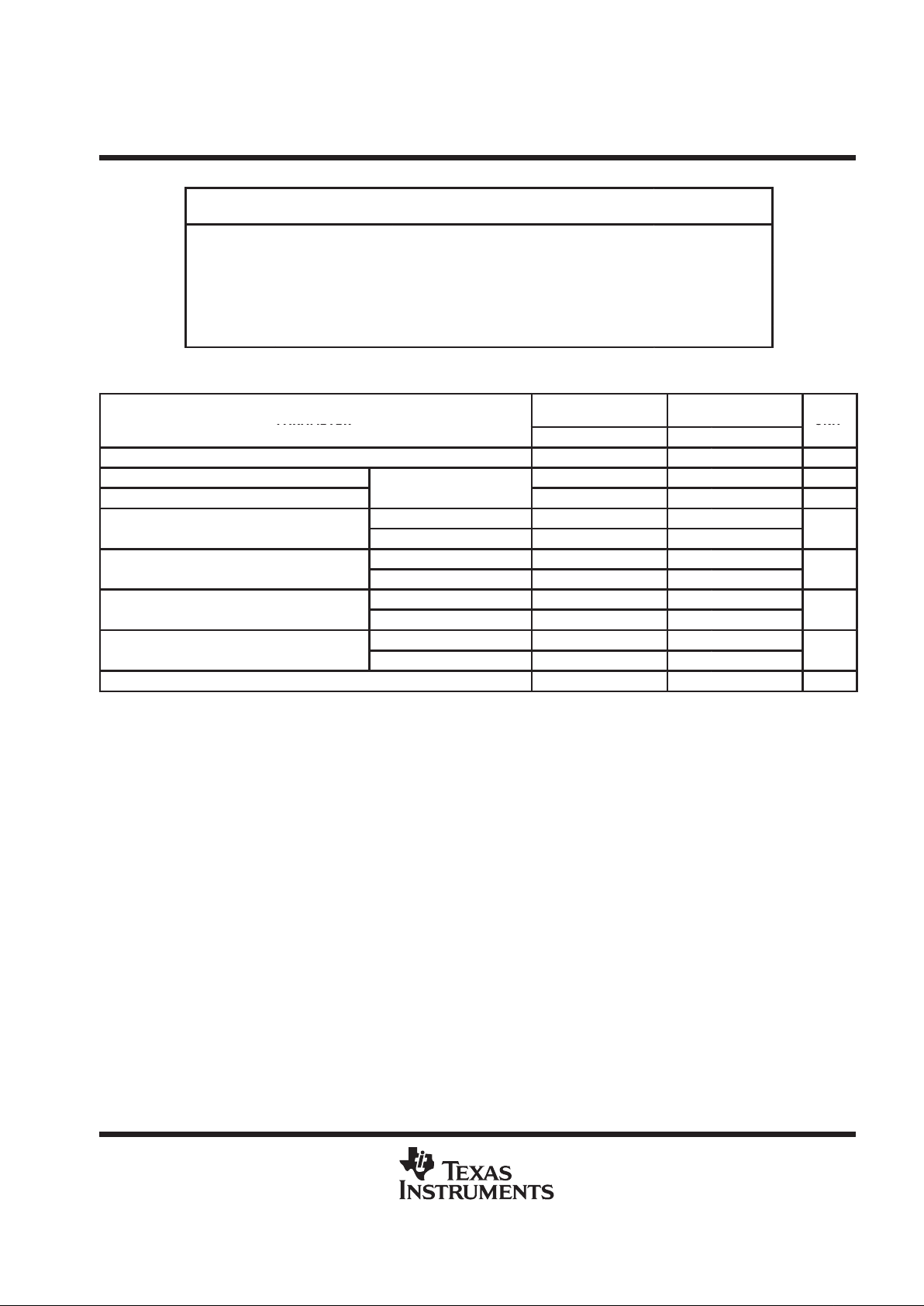
DISSIPATION RATING TABLE
PACKAGE
TA ≤ 25°C
POWER RATING
DERATING FACTOR
ABOVE TA = 25°C
TA = 70°C
POWER RATING
TA = 125°C
POWER RATING
D (8 pin) 725 mW 5.8 mW/°C 464 mW —
D (16 pin) 950 mW 7.6 mW/°C 608 mW —
FK 1375 mW 11.0 mW/°C 880 mW 275 mW
J 1375 mW 1 1.0 mW/°C 880 mW 275 mW
N 1150 mW 9.2 mW/°C 736 mW —
P 1000 mW 8.0 mW/°C 640 mW —
recommended operating conditions
PARAMETER
SN55116
SN75116, SN75117,
SN75118, SN75119
UNIT
PARAMETER
MIN NOM MAX MIN NOM MAX
UNIT
Supply voltage, V
CC
4.5 5 5.5 4.5 5 5.5 V
High-level input voltage, V
IH
All inputs except differential
2 2 V
Low-level input voltage, V
IL
inputs
0.8 0.8 V
p
Drivers –40 –40
High-level output current, I
OH
Receivers –5 –5
mA
p
Drivers 40 40
Low-level output current, I
OL
Receivers 15 15
mA
p
’116, SN75118 ±15 ±15
Receiver input voltage, V
I
SN75117, SN75119 0 6 0 6
V
p
’116, SN75118 ±15 ±15
Common-mode receiver input voltage, V
ICR
SN75117, SN75119 0 6 0 6
V
Operating free-air temperature, T
A
–55 125 0 70 °C

SN55116, SN75116, SN75117, SN75118, SN75119
DIFFERENTIAL LINE TRANSCEIVERS
SLLS073D – MAY 1976 – REVISED MAY 1998
6
POST OFFICE BOX 655303 DALLAS, TEXAS 75265
•
electrical characteristics over recommended operating free-air temperature range (unless otherwise noted)
driver section
’116, SN751 18 SN75117, SN751 19
PARAMETER
TEST CONDITIONS
†
MIN
TYP
‡
MAX MIN TYP‡MAX
UNIT
VIKInput clamp voltage VCC = MIN, II = –12 mA –0.9 –1.5 –0.9 –1.5 V
TA = 25°C (SN55116),
TA = 0°C to 70°C
IOH = –10 mA 2.4 3.4 2.4 3.4
VOHHigh-level output voltage
VCC = MIN,
VIL = 0.8 V,
A
(SN75116, SN75117,
SN75118, SN75119)
IOH = –40 mA 2 3 2 3
V
I
IH
= 2
V
T
= –55°C to 125°C
IOH = –10 mA 2 2
A
(SN55116)
IOH = –40 mA 1.8 1.8
VOLLow-level output voltage VCC = MIN, VIH = 2 V, VIL = 0.8 V, IOL = 40 mA 0.4 0.4 V
VOKOutput clamp voltage VCC = MAX, IO = –40 mA, DE at 0.8 V –1.5 –1.5 V
TA = 25°C 1 10
-
p
-
p
VCC = MAX,
SN55116 200
I
O(off)
Off-state o en-collector out ut current
VO = 12 V
TA = MAX
SN75116,
SN75118
20
µA
VCC = MAX, VO = 0 to V
CC,
DE at 0.8 V, TA = 25°C ±10
p
VO = 0 SN55116 –300
I
OZ
Off-state (high-impedance-state)
output current
V
CC
=
MAX
,
VO = 0.4 V to V
CC
SN55116 ±150
µA
DE at 0.8 V
,
TA = MAX
VO = 0 to V
CC
SN75116,
SN75118
±20
Input current at maximum
I
I
input voltage
Driver or
V
CC
=
MAX
,
V
I
= 5.5
V11
mA
I
IH
High-level input current
enable input
VCC = MAX, VI = 2.4 V 40 40 µA
I
IL
Low-level input current VCC = MAX, VI = 0.4 V –1.6 –1.6 mA
I
OS
Short-circuit output current
§
VCC = MAX, VO = 0, TA = 25°C –40 –120 –40 –120 mA
Supply current (driver and receiver
°
I
CC
y(
combined)
V
CC
=
MAX
,
T
A
=
25°C42604260
mA
†
All parameters with the exception of off-state open-collector output current are measured with the active pullup connected to the sink output. For conditions shown as MIN or MAX,
use the appropriate value specified under recommended operating conditions.
‡
All typical values are at VCC = 5 V and TA = 25°C.
§
Not more than one output should be shorted at a time, and duration of the short circuit should not exceed one second.

SN55116, SN75116, SN75117, SN75118, SN75119
DIFFERENTIAL LINE TRANSCEIVERS
SLLS073D – MAY 1976 – REVISED MAY 1998
7
POST OFFICE BOX 655303 • DALLAS, TEXAS 75265
switching characteristics, VCC = 5 V, CL = 30 pF, TA = 25°C
driver section
PARAMETER TEST CONDITIONS MIN TYP MAX UNIT
t
PLH
Propagation-delay time, low-to-high level output
14 30
t
PHL
Propagation-delay time, high-to-low level output
See Figure 13
12 30
ns
t
PZH
Output-enable time to high level RL = 180 Ω, See Figure 14 8 20 ns
t
PZL
Output-enable time to low level RL = 250 Ω, See Figure 15 17 40 ns
t
PHZ
Output-disable time from high level RL = 180 Ω, See Figure 14 16 30 ns
t
PLZ
Output-disable time from low level RL = 250 Ω, See Figure 15 20 35 ns

SN55116, SN75116, SN75117, SN75118, SN75119
DIFFERENTIAL LINE TRANSCEIVERS
SLLS073D – MAY 1976 – REVISED MAY 1998
8
POST OFFICE BOX 655303 DALLAS, TEXAS 75265
•
electrical characteristics over recommended operating free-air temperature range (unless otherwise noted)
receiver section
’116, SN751 18 SN75117, SN75119
PARAMETER
TEST CONDITIONS
†
MIN TYP‡MAX MIN TYP‡MAX
UNIT
VCC = MIN, V
ICR
= 0,
VO = 0.4 V, IOL = 15 mA,
CC ICR
See Note 4
0.5
0.5
V
IT+
Positive-going threshold voltage
§
O
See Note 3
OL
VCC = 5 V, V
ICR
= MAX,
V
CC ICR
See Note 5
1
1
VCC = MIN, V
ICR
= 0,
VO = 2.4 V, IOL = –5 mA,
CC ICR
See Note 4
–0.5
¶
–0.5
¶
V
IT–
Negative-going threshold voltage
§
O
See Note 3
OL
VCC = 5 V, V
ICR
= MAX,
V
CC ICR
See Note 5
–1
¶
–1
¶
15 6
V
I
Input voltage range
#
VCC = 5 V, VID = –1 V or 1 V, See Note 3
to
to
V
I
gg
CC
ID
–15 0
VCC = MIN, VID = –0.5 V,
p
IOH = –5 mA,
CC
V
ICR
= 0,
ID
See Notes 4 and 6
2.4
2.4
VOHHigh-level output voltage
OH
See Note 3
VCC = 5 V, VID = –1 V,
V
CC
V
ICR
= MAX,IDSee Note 5
2.4
2.4
VCC = MIN, VID = 0.5 V,
p
IOL = 15 mA,
CC
V
ICR
= 0,
ID
See Notes 4 and 7
0.4
0.4
VOLLow-level output voltage
OL
See Note 3
VCC = 5 V, VID = 1 V,
V
CC
V
ICR
= MAX,IDSee Note 5
0.4
0.4
VI = 0, Other input at 0 V –0.5 –0.9 –0.5 –1
I
I(rec)
Receiver input current
V
CC
=
MAX
,
VI = 0.4 V, Other input at 2.4 V –0.4 –0.7 –0.4 –0.8
mA
()
See Note 3
VI = 2.4 V, Other input at 0.4 V 0.1 0.3 0.1 0.4
VCC = MIN, VID = –0.5 V,
’
I
I
Input current at maximum
p
Strobe
CC ID
V
strobe
= 4.5 V
’116, SN75117
5
5µA
I
in ut voltage
Enable VCC = MAX, VI = 5.5 V SN75118, SN75119 1 1 mA
†
Unless otherwise noted, V
strobe
= 2.4 V. All parameters, with the exception of off-state open-collector output current, are measured with the active pullup connected to the sink output.
For conditions shown as MIN or MAX, use the appropriate value specified under recommended operating conditions.
‡
All typical values are at VCC = 5 V, TA = 25°C, and VIC = 0.
§
Differential voltages are at the B input terminal with respect to the A input terminal. Neither receiver input of the SN75117 or SN751 19 should be taken negative with respect to GND.
¶
The algebraic convention, where the less positive (more negative) limit is designated as minimum, is used in this data sheet for threshold voltages only.
#
Input voltage range is the voltage range that, if exceeded at either input, will cause the receiver to cease functioning properly.
NOTES: 3. Measurement of these characteristics on the SN75117 and SN75119 requires the driver to be disabled with the driver enable at 0.8 V.
4. This applies with the less positive receiver input grounded.
5. For ’116 and SN75118, this applies with the more positive receiver input at 15 V or the more negative receiver input at – 15 V. For SN75117 and SN751 19, this applies
with the more positive receiver input at 6 V.
6. For SN55116, VID = –1 V
7. For SN55116, VID = 1 V

SN55116, SN75116, SN75117, SN75118, SN75119
DIFFERENTIAL LINE TRANSCEIVERS
SLLS073D – MAY 1976 – REVISED MAY 1998
POST OFFICE BOX 655303 DALLAS, TEXAS 75265
• 9
receiver section (continued)
’116, SN751 18 SN75117, SN751 19
PARAMETER
TEST CONDITIONS
†
MIN TYP‡MAX MIN TYP‡MAX
UNIT
I
IH
High-level input current Enable VCC = MAX, VI = 2.4 V SN75118, SN75119 40 40 µA
V
= MAX, V
= 0.5 V,
’
I
I
Low-level input current
Strobe
CC
,
V
strobe
= 0.4 V,
ID
,
See Notes 4 and 7
’116, SN75117
–2.
4–2.4
mA
I
Enable VCC = MAX, VI = 0.4 V SN75118, SN75119 –1.6 –1.6
p
V
= MAX, V
= 0.5 V,
°
I
(RTC)
Response-time-control current (RTC)
CC
,
RC at 0 V,
ID
,
See Notes 4 and 7
T
A
=
25°C–1.2
mA
=
TA = 25°C 1 10
I
O(off)
Off-state open-collector output current
V
CC
=
MAX
,
VO = 12 V,
SN55116 200
µA
()
VID = – 1 V
T
A
=
MAX
SN75116, SN75118 20
=
TA = 25°C SN75118, SN75119 ±10 ±10
I
OZ
Off-state (high-impedance-state)
p
V
CC
=
MAX
,
VO = 0 to VCC,
SN75118 ±20
µA
out ut current
RE at 0.4 V
T
A
=
MAX
SN75119 ±20
R
T
Line-terminating resistance VCC = 5 V TA = 25°C 77 167 Ω
V
= MAX, V
= 0,
°
I
OS
Short-circuit output current
§
CC
,
VID = – 0.5 V,
O
,
See Notes 4 and 6
T
A
=
25°C–15–80–15–80
mA
Short current (driver and V
= MAX, V
= 0.5 V,
°
I
CC
(
receiver combined)
CC
,
ID
,
See Notes 4 and 7
T
A
=
25°C42604260
mA
†
Unless otherwise noted, V
strobe
= 2.4 V. All parameters, with the exception of of f-state open-collector output current, are measured with the active pullup connected to the sink output.
For conditions shown as MIN or MAX, use the appropriate value specified under recommended operating conditions.
‡
All typical values are at VCC = 5 V, TA = 25°C, and VIC = 0.
§
Not more than one output should be shorted at a time.
NOTES: 4. This applies with the less positive receiver input grounded.
6. For SN55116, VID = –1 V
7. For SN55116, VID = 1 V

SN55116, SN75116, SN75117, SN75118, SN75119
DIFFERENTIAL LINE TRANSCEIVERS
SLLS073D – MAY 1976 – REVISED MAY 1998
11
POST OFFICE BOX 655303 • DALLAS, TEXAS 75265
switching characteristics, VCC = 5 V, CL = 30 pF, TA = 25°C
receiver section
PARAMETER TEST CONDITIONS MIN TYP MAX UNIT
t
PLH
Propagation-delay time, low-to-high-level output
20 75 ns
t
PHL
Propagation-delay time, high-to-low-level output
R
L
=
400 Ω
,
See Figure 16
17 75 ns
t
PZH
Output-enable time to high level
RL = 480 Ω, See Figure 14 9 20 ns
t
PZL
Output-enable time to low level
SN75118
and
RL = 250 Ω, See Figure 15 16 35 ns
t
PHZ
Output-disable time from high level
SN75119
RL = 480 Ω, See Figure 14 12 30 ns
t
PLZ
Output-disable time from low level
only
RL = 250 Ω, See Figure 15 17 35 ns

SN55116, SN75116, SN75117, SN75118, SN75119
DIFFERENTIAL LINE TRANSCEIVERS
SLLS073D – MAY 1976 – REVISED MAY 1998
12
POST OFFICE BOX 655303 • DALLAS, TEXAS 75265
TYPICAL CHARACTERISTICS
†
Figure 1
3
2
1
0
012
4
5
6
34
DRIVER
OUTPUT VOLTAGE
vs
INPUT VOLTAGE
VI – Input Voltage – V
VCC = 5.5 V
VCC = 5 V
VCC = 4.5 V
No Load
TA = 25°C
VO – Output Voltage – V
V
O
Figure 2
3
2
1
0
012
4
5
6
34
DRIVER
OUTPUT VOLTAGE
vs
INPUT VOLTAGE
VI – Input Voltage – V
TA = – 55°C
TA = 125°C
TA = 25°C
VCC = 5 V
No Load
VO – Output Voltage – V
V
O
Figure 3
0
VOH – High-Level Output Voltage – V
IOH – High-Level Output Current – mA
6
–100
0
–20 –40 –60 –80
1
2
3
4
5
TA = 25°C
VCC = 5 V
VCC = 4.5 V
DRIVER
HIGH-LEVEL OUTPUT VOLTAGE
vs
HIGH-LEVEL OUTPUT CURRENT
V
OH
VCC = 5.5 V
Figure 4
0.3
0.2
0.1
0
02040
0.4
0.5
0.6
50 80 100
120
VCC = 4.5 V
VCC = 5.5 V
VOL – Low-Level Output Voltage – V
IOL – Low-Level Output Current – mA
DRIVER
LOW-LEVEL OUTPUT VOLTAGE
vs
LOW-LEVEL OUTPUT CURRENT
TA = 25°C
V
OL
†
Operation of the device at these or any other conditions beyond those indicated under ‘‘recommended operating conditions” is not implied.

SN55116, SN75116, SN75117, SN75118, SN75119
DIFFERENTIAL LINE TRANSCEIVERS
SLLS073D – MAY 1976 – REVISED MAY 1998
13
POST OFFICE BOX 655303 • DALLAS, TEXAS 75265
TYPICAL CHARACTERISTICS
†
Figure 5
– Propagation Delay Time – ns
DRIVER
PROPAGATION-DELAY TIME
vs
FREE-AIR TEMPERATURE
TA – Free-Air Temperature – °C
10
8
4
2
0
18
6
14
12
16
20
–75 0 25 50 75 100 125
t
PLH
t
PHL
VCC = 5 V
See Figure 13
CL = 30 pF
–50 –25
t
pd
Figure 6
Output Enable and Disable Time – ns
20
10
5
0
25
15
30
–75 0 25 50 75 100 125
TA – Free-Air Temperature – °C
t
PLZ
t
PZH
t
PHZ
t
PZL
DRIVER
OUTPUT-ENABLE AND DISABLE TIME
vs
FREE-AIR TEMPERATURE
See Note A
VCC = 5 V
–50 –25
NOTE A: For t
PZH
and t
PHZ
: RL = 480 Ω, see Figure 14. For t
PZL
and t
PLZ
: RL = 250 Ω, see Figure 15.
Figure 7
VCC = 5.5 V
RECEIVER
OUTPUT VOLTAGE
vs
DIFFERENTIAL INPUT VOLTAGE
–0.2
VO – Output Voltage – V
VID – Differential Input Voltage – V
6
0.2
0
–0.1 0 0.1
1
2
3
4
5
VCC = 4.5 V
Load = 2 kΩ to V
CC
TA = 25°C
V
O
VCC = 5 V
Figure 8
RECEIVER
OUTPUT VOLTAGE
vs
DIFFERENTIAL INPUT VOLTAGE
–0.2
VO – Output Voltage – V
6
0.2
0
–0.1
0 0.1
1
2
3
4
5
VID – Differential Input Voltage – V
TA = 25°C
TA = 125°C
TA = –55°C
VCC = 5 V
Load = 2 kΩ to V
CC
V
O
†
Operation of the device at these or any other conditions beyond those indicated under ‘‘recommended operating conditions” is not implied.

SN55116, SN75116, SN75117, SN75118, SN75119
DIFFERENTIAL LINE TRANSCEIVERS
SLLS073D – MAY 1976 – REVISED MAY 1998
14
POST OFFICE BOX 655303 • DALLAS, TEXAS 75265
TYPICAL CHARACTERISTICS
†
Figure 9
RECEIVER
PROPAGATION-DELAY TIME
vs
FREE-AIR TEMPERATURE
TA – Free-Air Temperature – °C
t
PLH
t
PHL
20
10
5
0
25
15
30
–75 0 25 50 75 100 125
VCC = 5 V
RL = 400 Ω
See Figure 16
–50 –25
– Propagation Delay Time – ns
t
pd
Figure 10
Output Enable and Disable Time – ns
20
10
5
0
25
15
30
–75 0 25 50 75 100 125
TA – Free-Air Temperature – °C
t
PLZ
t
PZH
t
PHZ
t
PZL
RECEIVER
OUTPUT-ENABLE AND DISABLE TIME
vs
FREE-AIR TEMPERATURE
See Note A
VCC = 5 V
–50 –25
NOTE A: For t
PZH
and t
PHZ
:RL= 480 Ω, see Figure 14. For t
PZL
and t
PLZ
: RL = 250 Ω, see Figure 15.
Figure 11
40
20
10
0
012 3 45
60
70
80
678
50
30
ICC – Supply Current – mA
VCC – Supply Voltage – V
DRIVER AND RECEIVER
SUPPLY CURRENT
vs
SUPPLY VOLTAGE
No Load
TA = 25°C
CC
I
Figure 12
DRIVER AND RECEIVER
SUPPLY CURRENT
vs
FREE-AIR TEMPERATURE
ICC – Supply Current – mA
TA – Free-Air Temperature – °C
VCC = 5 V
25
20
10
5
0
45
15
35
30
40
50
–75 0 25 50 75 100 125
CC
I
–50 –25
†
Operation of the device at these or any other conditions beyond those indicated under ‘‘recommended operating conditions” is not implied.

SN55116, SN75116, SN75117, SN75118, SN75119
DIFFERENTIAL LINE TRANSCEIVERS
SLLS073D – MAY 1976 – REVISED MAY 1998
15
POST OFFICE BOX 655303 • DALLAS, TEXAS 75265
PARAMETER MEASUREMENT INFORMATION
Figure 13
From Output
Under Test
Test
Point
CL = 30 pF
(see Note A)
LOAD CIRCUIT
≤ 5 ns
Input
10%
90%
1.5 V
3 V
0 V
NAND
Output
AND
Output
t
PLH
t
PHL
VOLTAGE WAVEFORMS
V
OH
V
OL
V
OH
V
OL
t
PHL
t
PLH
1.5 V
1.5 V
90%
10%
≤ 5 ns
1.5 V
1.5 V 1.5 V
t
PLH
and t
PHL
(drivers only)
Figure 14
RL = 180 Ω
3 V
0 V
0.5 V
t
PZH
V
OH
V
off
= 0 V
t
PHZ
Input
Output
VOLTAGE WAVEFORMS
LOAD CIRCUIT
From Output
Under Test
CL = 30 pF
(see Note A)
Test
Point
≤ 5 ns ≤ 5 ns
90%
90%
1.5 V 1.5 V
10% 10%
1.5 V
t
PZH
and t
PHZ
Figure 15
From Output
Under Test
Test
Point
CL = 30 pF
(see Note A)
RL = 250 Ω
5 V
VOLTAGE WAVEFORMS
LOAD CIRCUIT
V
OL
V
off
= 5 V
0.5 V
1.5 V
10% 10%
90% 90%
≤ 5 ns
0 V
3 V
1.5 V
t
PZL
t
PLZ
Input
Output
≤ 5 ns
1.5 V
t
PZL
and t
PLZ
(SN75118 and SN75119 receivers only)
Figure 16
RL = 400 Ω
5 V
See Note B
LOAD CIRCUIT
VOLTAGE WAVEFORMS
Output
10% 10%
See Note C
V
L
V
H
V
OH
V
OL
t
PHL
t
PLH
B Input
see Note C)
Test
Point
From Output
Under Test
CL = 30 pF
(see Note A)
≤ 5 ns ≤ 5 ns
90%
50%
90%
50%
1.5 V 1.5 V
t
PLH
and t
PHL
(receivers only)
NOTES: A. CL includes probe and jig capacitance.
B. All diodes are 1N3064 or equivalent.
C. For ’116 and SN75118, VH = 3 V, VL = – 3 V, the A input is at 0 V.
For SN75117 and SN75119, VH = 3 V, VL = 0, the A input is at 1.5 V.
D. When testing the ’116 and SN75118 receiver sections, the response-time control and the termination resistor pins are left open.

IMPORTANT NOTICE
T exas Instruments and its subsidiaries (TI) reserve the right to make changes to their products or to discontinue
any product or service without notice, and advise customers to obtain the latest version of relevant information
to verify, before placing orders, that information being relied on is current and complete. All products are sold
subject to the terms and conditions of sale supplied at the time of order acknowledgement, including those
pertaining to warranty, patent infringement, and limitation of liability.
TI warrants performance of its semiconductor products to the specifications applicable at the time of sale in
accordance with TI’s standard warranty. Testing and other quality control techniques are utilized to the extent
TI deems necessary to support this warranty. Specific testing of all parameters of each device is not necessarily
performed, except those mandated by government requirements.
CERT AIN APPLICATIONS USING SEMICONDUCTOR PRODUCTS MA Y INVOLVE POTENTIAL RISKS OF
DEATH, PERSONAL INJURY, OR SEVERE PROPERTY OR ENVIRONMENTAL DAMAGE (“CRITICAL
APPLICATIONS”). TI SEMICONDUCTOR PRODUCTS ARE NOT DESIGNED, AUTHORIZED, OR
WARRANTED TO BE SUITABLE FOR USE IN LIFE-SUPPORT DEVICES OR SYSTEMS OR OTHER
CRITICAL APPLICATIONS. INCLUSION OF TI PRODUCTS IN SUCH APPLICA TIONS IS UNDERST OOD TO
BE FULLY AT THE CUSTOMER’S RISK.
In order to minimize risks associated with the customer’s applications, adequate design and operating
safeguards must be provided by the customer to minimize inherent or procedural hazards.
TI assumes no liability for applications assistance or customer product design. TI does not warrant or represent
that any license, either express or implied, is granted under any patent right, copyright, mask work right, or other
intellectual property right of TI covering or relating to any combination, machine, or process in which such
semiconductor products or services might be or are used. TI’s publication of information regarding any third
party’s products or services does not constitute TI’s approval, warranty or endorsement thereof.
Copyright 1998, Texas Instruments Incorporated
 Loading...