

SN55115, SN75115
DUAL DIFFERENTIAL RECEIVERS
SLLS072D – SEPTEMBER 1973 – REVISED MA Y 1998
1
POST OFFICE BOX 655303 • DALLAS, TEXAS 75265
D
Choice of Open-Collector or Active Pullup
(Totem-Pole) Outputs
D
Single 5-V Supply
D
Differential Line Operation
D
Dual-Channel Operation
D
TTL Compatible
D
±15-V Common-Mode Input Voltage Range
D
Optional-Use Built-In 130-Ω LineT erminating Resistor
D
Individual Frequency-Response Controls
D
Individual Channel Strobes
D
Designed for Use With SN55113, SN75113,
SN55114, and SN75114 Drivers
D
Designed to Be Interchangeable With
National DS9615 Line Receivers
description
The SN55115 and SN75115 dual differential line
receivers are designed to sense small differential
signals in the presence of large common-mode
noise. These devices give TTL-compatible output
signals as a function of the differential input
voltage. The open-collector output configuration
permits the wire-ANDing of similar TTL outputs
(such as SN5401/SN7401) or other
SN55115/SN75115 line receivers. This permits a
level of logic to be implemented without extra
delay.
The output stages are similar to TTL totem-pole outputs, but with sink outputs, 1YS and 2YS, and the
corresponding active pullup terminals, 1YP and 2YP, available on adjacent package pins. The frequency
response and noise immunity may be provided by a single external capacitor. A strobe input is provided for each
channel. With the strobe in the low level, the receiver is disabled and the outputs are forced to a high level.
The SN55115 is characterized for operation over the full military temperature range of –55°C to 125°C. The
SN75115 is characterized for operation from 0°C to 70°C.
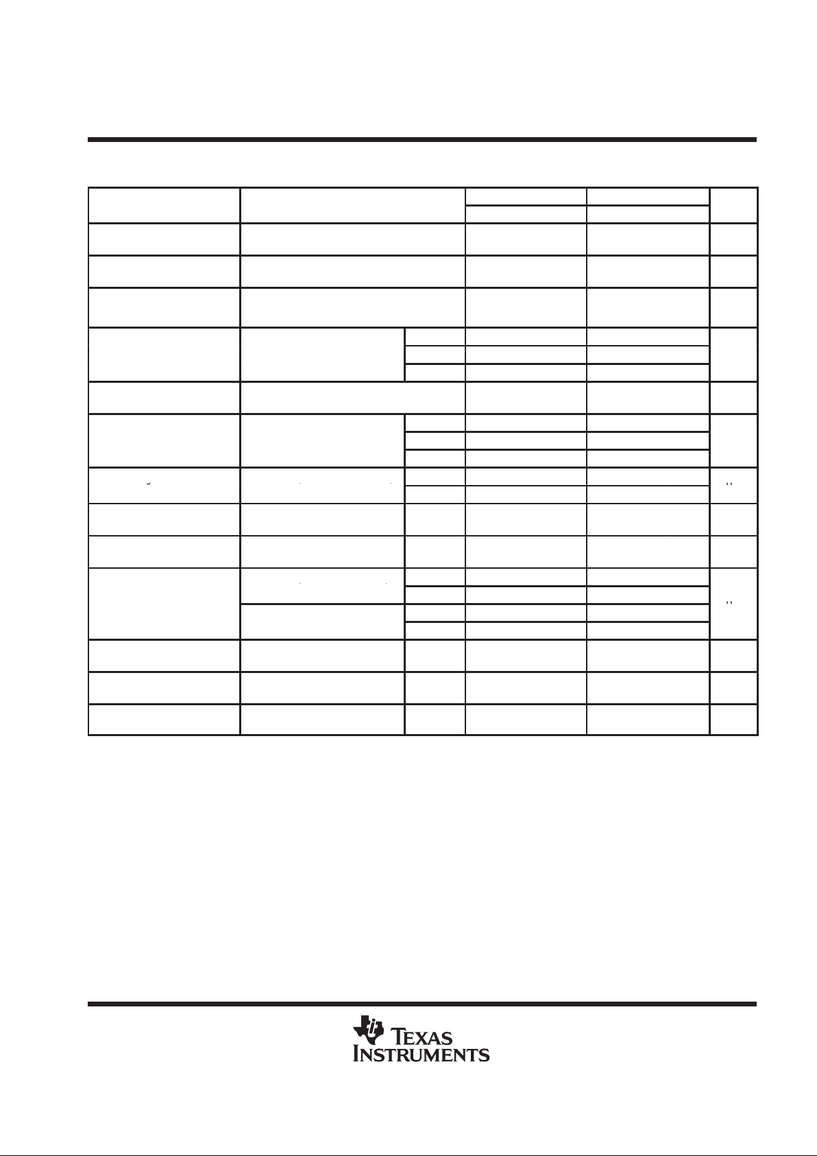
FUNCTION TABLE
STRB
DIFF INPUT
(A AND B)
OUTPUT
(YP AND YS
TIED
TOGETHER)
L X H
H LH
HHL
H = VI ≥ VIH min or VID more positive than VT+ max
L = VI ≤ VIL max or VID more negative thanV
T–
max
X = irrelevant
Copyright 1998, Texas Instruments Incorporated
PRODUCTION DATA information is current as of publication date.
Products conform to specifications per the terms of Texas Instruments
standard warranty. Production processing does not necessarily include
testing of all parameters.
Please be aware that an important notice concerning availability, standard warranty, and use in critical applications of
Texas Instruments semiconductor products and disclaimers thereto appears at the end of this data sheet.
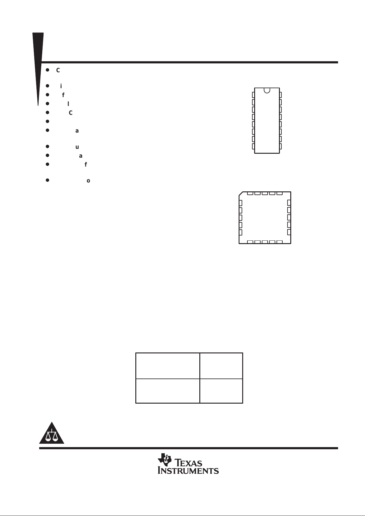
1
2
3
4
5
6
7
8
16
15
14
13
12
11
10
9
1YS
1YP
1STRB
1RTC
1B
1R
T
1A
GND
V
CC
2YS
2YP
2STRB
2RTC
2B
2R
T
2A
SN55115 ...J OR W PACKAGE
SN75115 ...N PACKAGE
(TOP VIEW)
3212019
910111213
4
5
6
7
8
18
17
16
15
14
2YP
2STRB
NC
2RTC
2B
1STRB
1RTC
NC
1B
1R
T
SN55114 . . . FK PACKAGE
(TOP VIEW)
1YP
1YSNC2YS
1A
GND
NC
NC – No internal connection
CC
V
2A
2R
T
SN55115, SN75115
DUAL DIFFERENTIAL RECEIVERS
SLLS072D – SEPTEMBER 1973 – REVISED MA Y 1998
2
POST OFFICE BOX 655303 • DALLAS, TEXAS 75265
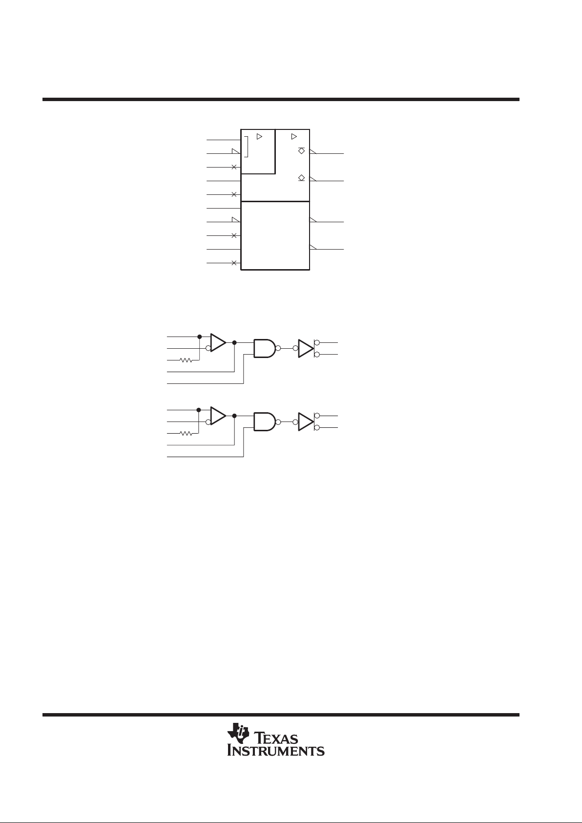
logic symbol
†
&
2YS
2YP
1YS
1YP
R
T
RSP
12
13
10
9
11
4
3
6
7
5
2RTC
2STRB
2R
T
2A
2B
1RTC
1STRB
1R
T
1A
1B
15
14
1
2
†
This symbol is in accordance with ANSI/IEEE Std 91-1984 and IEC Publication 617-12.
logic diagram (positive logic)
11
9
10
12
13
2YP (Pullup)
2YS (Sink)
14
15
2B
2A
2R
T
2RTC
2STRB
1STRB
1RTC
1R
T
1A
1B
1
2
1YP (Pullup)
3
4
6
7
5
1YS (Sink)
SN55115, SN75115
DUAL DIFFERENTIAL RECEIVERS
SLLS072D – SEPTEMBER 1973 – REVISED MA Y 1998
3
POST OFFICE BOX 655303 • DALLAS, TEXAS 75265
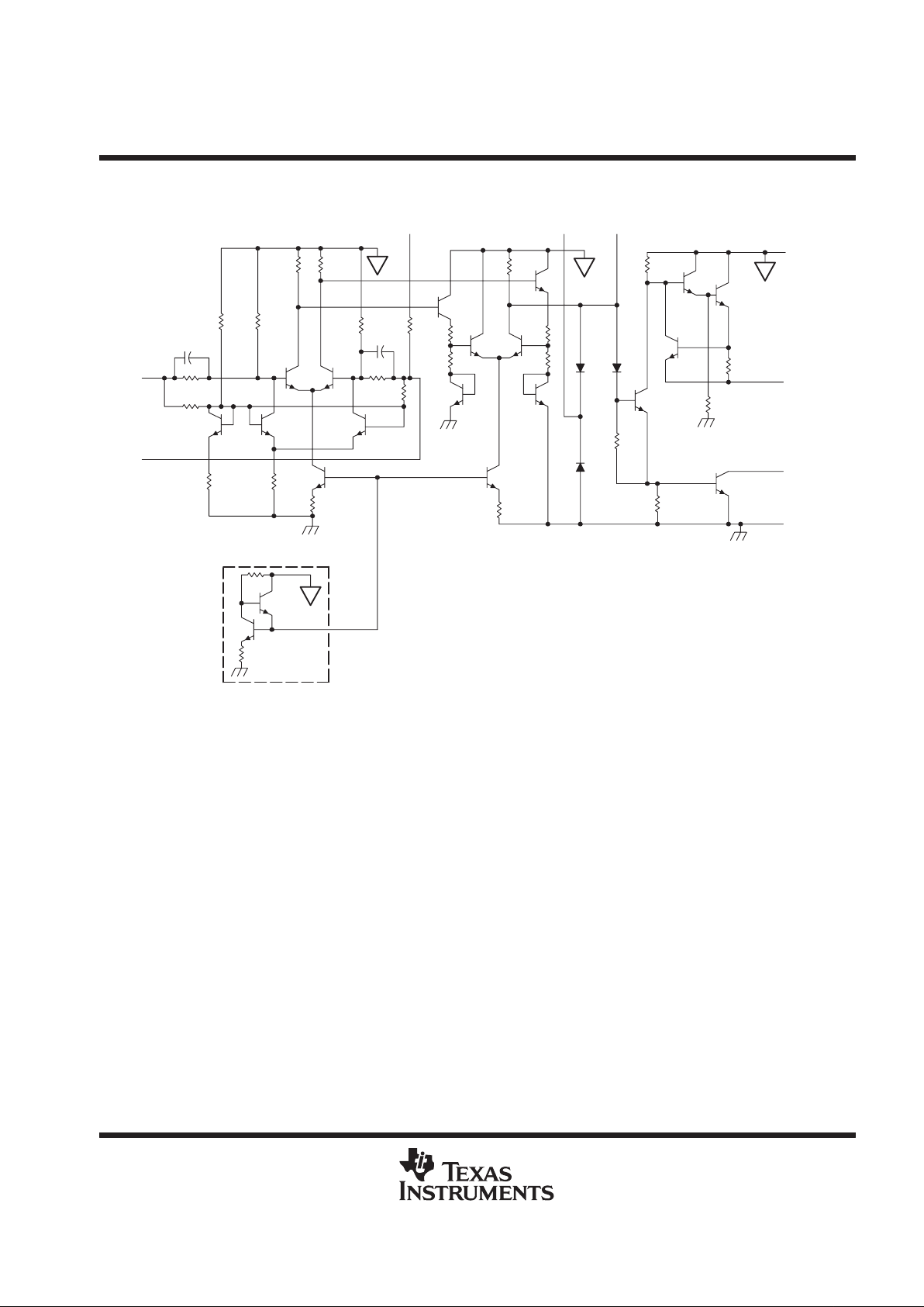
schematic (each receiver)
YS
Sink
1.64 k 130
Input 7.9
V
V
V
V
150
2.5 k
Common to
Both Receivers
A
8 k
7 k
1 pF
1.5 k 1.64 k
B
Input 5.11
130 150
150
8 k
7 k
1 pF
1 k 1 k
2.6 k
500
2.6 k
500
150
1.5 k
3 k
5 k
20
2 k
R
T
6,10
Strobe
3,13
Response
Time
Control
4,12
2.7 k
16
V
CC
2,14 Pullup
YP
1,15
Output
8
GND
Resistor values are nominal and in ohms.
Pin numbers shown are for the J, N, and W packages.
absolute maximum ratings over operating free-air temperature range (unless otherwise noted)
†
Supply voltage, V
CC
(see Note 1) 7 V. . . . . . . . . . . . . . . . . . . . . . . . . . . . . . . . . . . . . . . . . . . . . . . . . . . . . . . . . . . . .
Input voltage V
I
(A, B, and RT) ±25 V. . . . . . . . . . . . . . . . . . . . . . . . . . . . . . . . . . . . . . . . . . . . . . . . . . . . . . . . . . . . . .
Input voltage V
I
(STRB) 5.5 V. . . . . . . . . . . . . . . . . . . . . . . . . . . . . . . . . . . . . . . . . . . . . . . . . . . . . . . . . . . . . . . . . . . .
Off-state voltage applied to open-collector outputs 14 V. . . . . . . . . . . . . . . . . . . . . . . . . . . . . . . . . . . . . . . . . . . . .
Continuous total power dissipation See Dissipation Rating Table. . . . . . . . . . . . . . . . . . . . . . . . . . . . . . . . . . . . .
Storage temperature range, T
stg
–65°C to 150°C. . . . . . . . . . . . . . . . . . . . . . . . . . . . . . . . . . . . . . . . . . . . . . . . . . .
Case temperature for 60 seconds: FK package 260°C. . . . . . . . . . . . . . . . . . . . . . . . . . . . . . . . . . . . . . . . . . . . . .
Lead temperature 1,6 mm (1/16 inch) from case for 60 seconds: J or W package 300°C. . . . . . . . . . . . . . . .
Lead temperature 1,6 mm (1/16 inch) from case for 10 seconds: N package 260°C. . . . . . . . . . . . . . . . . . . . .
†
Stresses beyond those listed under “absolute maximum ratings” may cause permanent damage to the device. These are stress ratings only, and
functional operation of the device at these or any other conditions beyond those indicated under “recommended operating conditions” is not
implied. Exposure to absolute-maximum-rated conditions for extended periods may affect device reliability.
NOTE 1: All voltage values, except differential input voltage, are with respect to network ground terminal.
SN55115, SN75115
DUAL DIFFERENTIAL RECEIVERS
SLLS072D – SEPTEMBER 1973 – REVISED MA Y 1998
4
POST OFFICE BOX 655303 • DALLAS, TEXAS 75265
DISSIPATION RATING TABLE
PACKAGE
TA ≤ 25°C
POWER RATING
DERATING FACTOR
ABOVE TA = 25°C
TA = 70°C
POWER RATING
TA = 125°C
POWER RATING
FK
†
1375 mW 11.0 mW/°C 880 mW 275 mW
J
†
1375 mW 11.0 mW/°C 880 mW 275 mW
N 1150 mW 9.2 mW/°C 736 mW —
W
†
1000 mW 8.0 mW/°C 640 mW 200 mW
†
In the FK, J, and W packages, SN55115 chips are either silver glass or alloy mounted. SN75115 chips are
glass mounted.
recommended operating conditions
SN55115 SN75115
MIN NOM MAX MIN NOM MAX
UNIT
Supply voltage, V
CC
4.5 5 5.5 4.75 5 5.25 V
High-level input voltage at STRB, V
IH
2.4 2.4 V
Low-level input voltage at STRB, V
IL
0.4 0.4 V
High-level output current, I
OH
–5 –5 mA
Low-level output current, I
OL
15 15 mA
Operating free-air temperature, T
A
–55 125 0 70 °C
SN55115, SN75115
DUAL DIFFERENTIAL RECEIVERS
SLLS072D – SEPTEMBER 1973 – REVISED MA Y 1998
5
POST OFFICE BOX 655303 • DALLAS, TEXAS 75265
electrical characteristics over recommended operating free-air temperature range (unless
otherwise noted)
SN55115 SN75115
PARAMETER
TEST CONDITIONS
†
MIN TYP‡MAX MIN TYP‡MAX
UNIT
V
IT+
§
Positive-going
threshold voltage
VO = 0 .4 V, IOL = 15 mA, VIC = 0 500 500 mV
V
IT–
§
Negative-going
threshold voltage
VO = 2 .4 V, IOH = –5 mA, VIC = 0
–500
¶
–500
¶
mV
V
ICR
Common-mode
input voltage range
VID = ±1 V
+15
to
–15
+24
to
–19
+15
to
–15
+24
to
–19
V
TA = MIN 2.2 2.4
V
OH
High-level ouput
VCC = MIN,
–
VID = –0.5 V,
TA = 25°C
2.4 3.4 2.4 3.4
V
voltage
I
OH
= –5
mA
TA = MAX 2.4 2.4
V
OL
Low-level output
voltage
VCC = MIN,
IOL = 15 mA
VID = –0.5 V,
0.22 0.4 0.22 0.45 V
TA = MIN –0.9 –0.9
I
IL
Low-level input
VCC = MAX, VI = 0.4 V,
p
TA = 25°C –0.5 –0.7 –0.5 –0.7
mA
current
Other in ut at 5.5 V
TA = MAX –0.7 –0.7
High-level strobe V
= MIN, V
= –0.5 V,
TA = 25°C 2 5
I
SH
g
current
CC
,
V
strobe
= 4.5 V
ID
,
TA = MAX 5 10
µ
A
I
SL
Low-level strobe
current
VCC = MAX,
V
strobe
= 0.4 V
VID = 0.5 V,
TA = 25°C –1.15 –2.4 –1.15 –2.4 mA
I(
RTC)
Response-timecontrol current
VCC = MAX,
VRC = 0
VID = 0.5 V,
TA = 25°C –1.2 –3.4 –1.2 –3.4 mA
V
= MIN, V
= 12 V,
TA = 25°C 100
Off-state
p
CC
,
VID = –4.5 V
OH
,
TA = MAX 200
IO(off)
open-collector
o
utput curre
nt
V
= MIN, V
= 5.25 V ,
TA = 25°C 100
µ
A
out ut current
CC
,
VID = –4.75 V
OH
,
TA = MAX 200
R
T
Line-terminating
resistance
VCC = 5 V TA = 25°C 77 130 167 74 130 179 Ω
I
OS
Supply-circuit output
current
#
VCC = MAX,
VO = 0
VID = –0.5 V,
TA = 25°C –15 –40 –80 –14 –40 –100 mA
I
CC
Supply current
(both receivers)
VCC = MAX,
VIC = 0
VID = 0.5 V,
TA = 25°C 32 50 32 50 mA
†
Unless otherwise noted, V
strobe
= 2.4 V. All parameters with the exception of of f-state open-collector output current are measured with the active
pullup connected to the sink output.
‡
All typical values are at VCC = 5 V, TA = 25°C, and VIC = 0.
§
Differential voltages are at the B input terminal with respect to the A input terminal.
¶
The algebraic convention, in which the less positive (more negative) limit is designated as minimum, is used in this data sheet for threshold
voltages only.
#
Only one output should be shorted to ground at a time, and duration of the short circuit should not exceed one second.
SN55115, SN75115
DUAL DIFFERENTIAL RECEIVERS
SLLS072D – SEPTEMBER 1973 – REVISED MA Y 1998
6
POST OFFICE BOX 655303 • DALLAS, TEXAS 75265
switching characteristics, VCC = 5 V, CL = 30 pF, TA = 25°C
SN55115 SN75115
PARAMETER
TEST CONDITIONS
MIN TYP MAX MIN TYP MAX
UNIT
t
PLH
Propagation delay time,
low-to-high level output
RL = 3.9 kΩ, See Figure 1 18 50 18 75 ns
t
PHL
Propagation delay time,
high-to-low level output
RL = 390 Ω, See Figure 1 20 50 20 75 ns
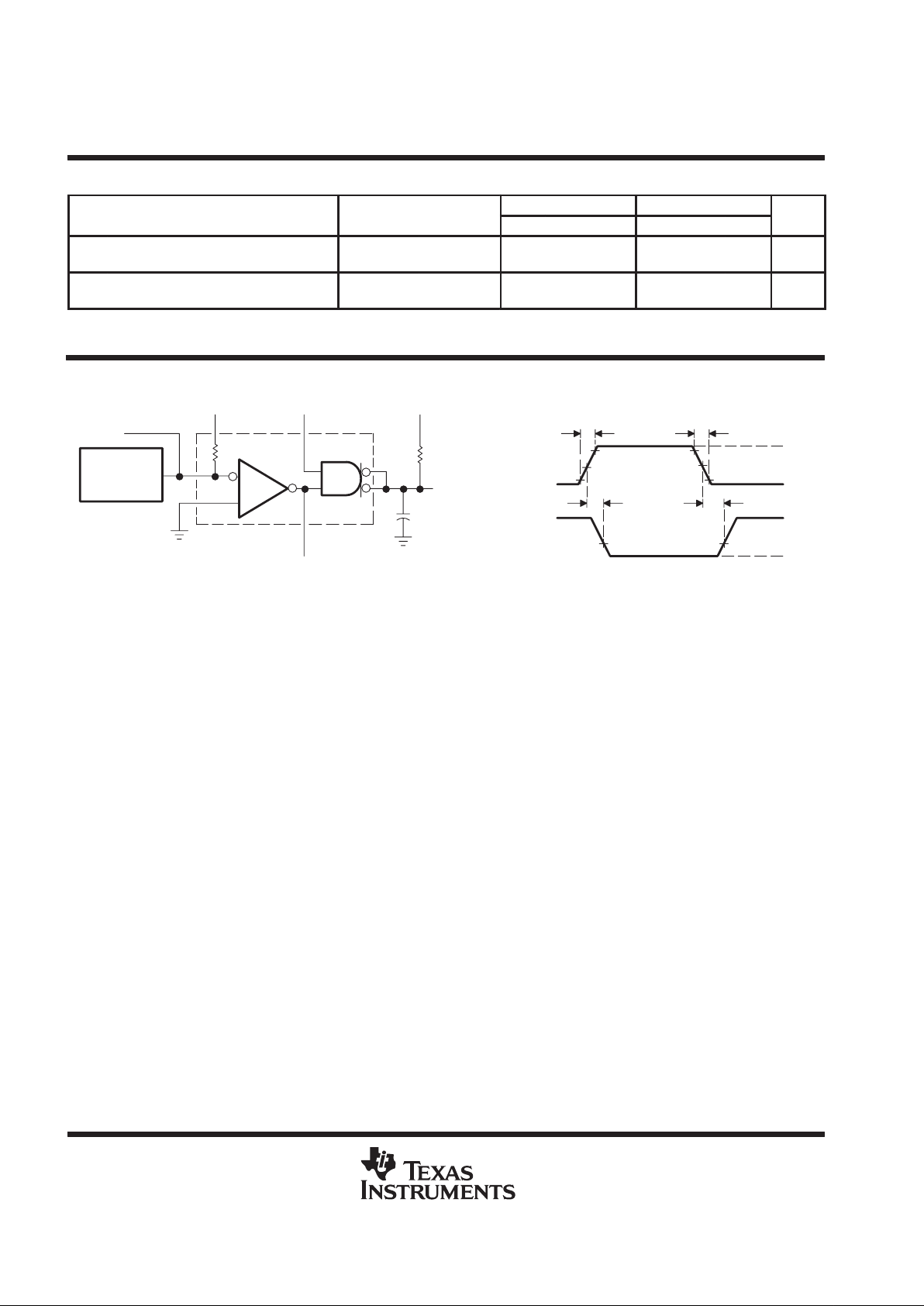
PARAMETER MEASUREMENT INFORMATION
STRB
90%
0 V
0 V
10%
90%
≤ 5 ns ≤ 5 ns
t
PHL
1.5 V
V
OL
V
OH
–3 V
3 V
Output
Differential
Input
t
PLH
1.5 V
V
O
R
L
5 V
YP
YS
CL = 30 pF
(see Note B)
Response
Time Control
Open
2.4 VOpen
R
T
B
A
Input
Pulse
Generator
(see Note A)
10%
TEST CIRCUIT VOLTAGE WAVEFORM
NOTES: A. The pulse generator has the following characteristics: ZO = 50 Ω, PRR ≤ 500 kHz, tw ≤ 100 ns, duty cycle = 50%.
B. CL includes probe and jig capacitance.
Figure 1. Test Circuit and Voltage Waveforms

SN55115, SN75115
DUAL DIFFERENTIAL RECEIVERS
SLLS072D – SEPTEMBER 1973 – REVISED MA Y 1998
7
POST OFFICE BOX 655303 • DALLAS, TEXAS 75265
TYPICAL CHARACTERISTICS
†
0
–2
–4
–6
–25 –20–15–10 –5 0 5
II – Input Current – mA
2
4
INPUT CURRENT
vs
INPUT VOLTAGE
6
10 15 20 25
VCC = 5 V
Input Not Under Test at 0 V
TA = 25°C
VI – Input Voltage – V
I
I
Figure 2
Figure 3
OUTPUT VOLTAGE
vs
FREE-AIR TEMPERATURE
ICC – Output Voltage – V
TA – Free-Air Temperature – °C
VCC = 4.5 V
2
1.6
0.8
0.4
0
3.4
1.2
2.8
2.4
3.2
4
– 75 – 50 – 25 0 25 50 75 100 125
VOH (VID = –0.5 V, IOH = –5 mA)
VOL (VID = 0.5 V, IOL = 15 mA)
CC
I
Figure 4
OUTPUT VOLTAGE
vs
COMMON-MODE INPUT VOLTAGE
3
2
1
0
–25–20–15 –10 –5 0 5
4
5
6
10 15 20 25
No Load
TA = 25°C
VCC = 5.5 V
VID = – 1 V
VID = 1 V
VCC = 5 V
VCC = 4.5 V
VO – Output Voltage – V
VIC – Common-Mode Input Voltage – V
V
O
†
Data for temperatures below 0°C and above 70°C and for supply voltages below 4.75 V and above 5.25 V are applicable to SN55115 circuits
only. These parameters were measured with the active pullup connected to the sink output.

SN55115, SN75115
DUAL DIFFERENTIAL RECEIVERS
SLLS072D – SEPTEMBER 1973 – REVISED MA Y 1998
8
POST OFFICE BOX 655303 • DALLAS, TEXAS 75265
TYPICAL CHARACTERISTICS
Figure 5
HIGH-LEVEL OUTPUT VOLTAGE
vs
HIGH-LEVEL OUTPUT CURRENT
2
1
0
0 –10
3
4
5
VID = –0.5 V
TA = 25°C
VCC = 5.5 V
VCC = 5 V
VCC = 4.5 V
VOH – High-Level Output Voltage – V
IOH – High-Level Output Current – mA
V
OH
–50
–40–30–20
Figure 6
VCC = 4.5 V
LOW-LEVEL OUTPUT VOLTAGE
vs
LOW-LEVEL OUTPUT CURRENT
0
VOL – Low-Level Output Voltge – V
IOL– Low-Level Output Current – mA
0.4
30
0
5 10 15 20 25
0.1
0.2
0.3
TA = 25°C
VCC = 5.5 V
V
OL
VID = 0.5 V
Figure 7
OUTPUT VOLTAGE
vs
DIFFERENTIAL INPUT VOLTAGE
–0.2
VO – Output Voltage – V
6
0.2
0
–0.1 0 0.1
1
2
3
4
5
TA = 125°C
TA = 25°C
TA = –55°C
VCC = 5 V
Load = 2 kΩ to V
CC
VID – Differential Input Voltage – V
V
O
Figure 8
OUTPUT VOLTAGE
vs
DIFFERENTIAL INPUT VOLTAGE
VO – Output Voltage – V
0.2–0.1 0 0.1
VCC = 5.5 V
VCC = 5 V
VCC = 4.5 V
–0.2
VID – Differential Input Voltage – V
6
0
1
2
3
4
5
Load = 2 kΩ to V
CC
TA = 25°C
V
O
–0.15 –0.05 0.5 0.15
SN55115, SN75115
DUAL DIFFERENTIAL RECEIVERS
SLLS072D – SEPTEMBER 1973 – REVISED MA Y 1998
9
POST OFFICE BOX 655303 • DALLAS, TEXAS 75265
TYPICAL CHARACTERISTICS
†
Figure 9
OUTPUT VOLTAGE
vs
STROBE INPUT VOLTAGE
0
VO – Output Voltage – V
V
strobe
– Strobe Input Voltage – V
6
4
0
1
2
3
4
5
123
V
CC
= 5.5 V
VCC = 5 V
VCC = 4.5 V
V
O
No Load
VID = 0.5 V
TA = 25°C
0.5 1.5 2.5 3.5
Figure 10
OUTPUT VOLTAGE
vs
STROBE INPUT VOLTAGE
0
VO – Output Voltage – V
V
strobe
– Strobe Input Voltage – V
6
4
0
1
2
3
4
5
123
T
A
= 125°C
TA = –55°C
TA = 25°C
V
O
VCC = 5 V
No Load
VID = 0.5 V
0.5 1.5 2.5 3.5
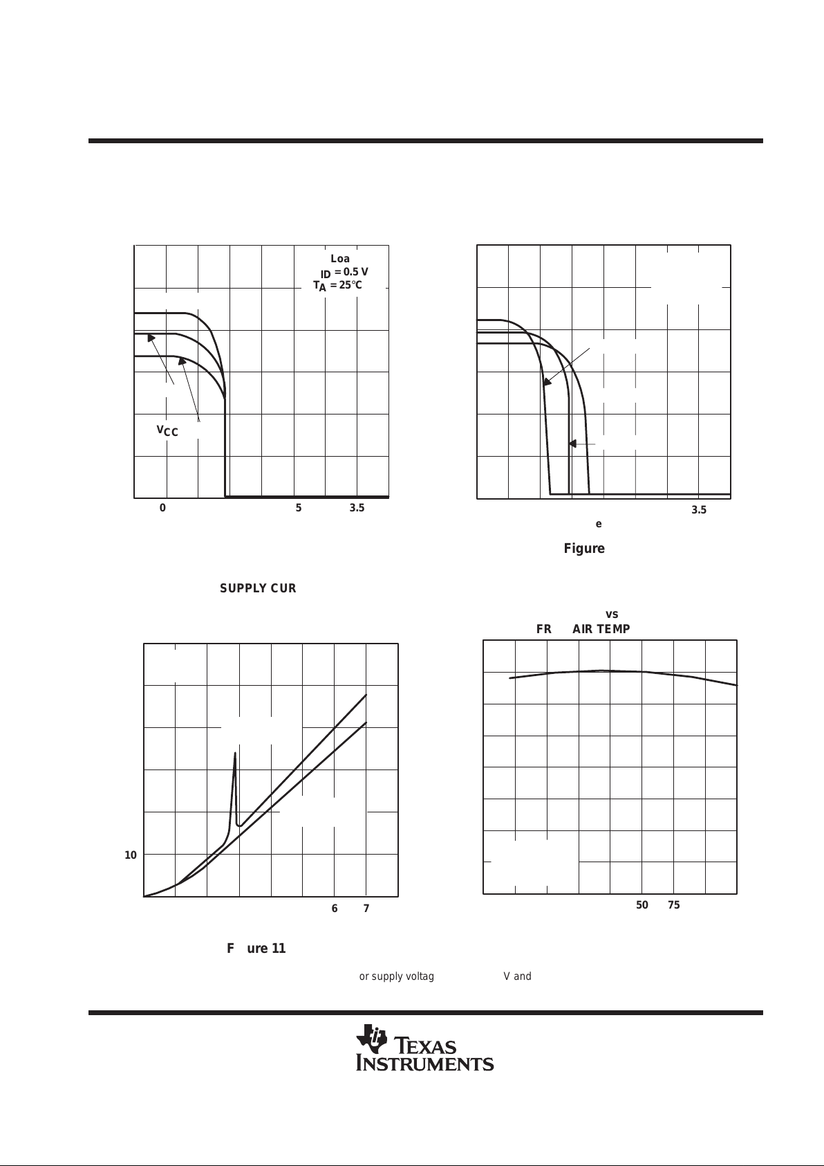
Figure 11
SUPPLY CURRENT
(BOTH RECEIVERS)
vs
SUPPLY VOLTAGE
0
ICC – Supply Current – mA
VCC – Supply Voltage – V
60
8
0
1234567
10
20
30
40
50
B Input at V
CC
A Input at 0 V
B Input at 0 V
A Input at V
CC
CC
I
No Load
TA = 25°C
Figure 12
SUPPLY CURRENT
(BOTH RECEIVERS)
vs
FREE-AIR TEMPERATURE
–75
ICC – Supply Current – mA
TA – Free-Air Temperature – °C
40
125
0
–50 –25 0 25 50 75 100
5
10
15
20
25
30
35
VCC = 5.5 V
B Input at 5.5 V
A Input at 0 V
CC
I
†
Data for temperatures below 0°C and above 70°C and for supply voltages below 4.75 V and above 5.25 V are applicable to SN55115 circuits
only. These parameters were measured with the active pullup connected to the sink output.

SN55115, SN75115
DUAL DIFFERENTIAL RECEIVERS
SLLS072D – SEPTEMBER 1973 – REVISED MA Y 1998
10
POST OFFICE BOX 655303 • DALLAS, TEXAS 75265
TYPICAL CHARACTERISTICS
†
Figure 13
PROPAGATION DELAY TIMES
vs
FREE-AIR TEMPERATURE
–75
Propagation Delay Times – ns
TA – Free-Air Temperature – °C
30
125
0
–50 –25 0 25 50 75 100
5
10
15
20
25
VCC = 5 V
See Figure 1
t
PHL
(RL = 390 Ω)
t
PLH
(RL = 3.9 kΩ)
Figure 14
MAXIMUM OPERATING FREQUENCY
vs
RESPONSE-TIME-CONTROL CAPACITANCE
0.001
fmax – Maximum Operating Frequency – Hz
Response-Time-Control Capacitance – µF
10M
10
100
0.01 0.1 1
1k
10k
1M
VCC = 5 V
Input: – 0.5-V to 0.5-V Square Wave
TA = 25°C
max
f
†
Data for temperatures below 0°C and above 70°C and for supply voltages below 4.75 V and above 5.25 V are applicable to SN55115 circuits
only. These parameters were measured with the active pullup connected to the sink output.
APPLICATION INFORMATION
Location 1
SN75113 Driver
SN75115 Receiver
Location 3
Location 2
Location 5
Location 4
Location 6
Twisted
Pair
Z
O
‡
Z
O
‡
‡
ZO = RT. A capacitor may be connected in series with ZO to reduce power dissipation.
Figure 15. Basic Party-Line or Data-Bus Differential Data Transmission

IMPORTANT NOTICE
T exas Instruments and its subsidiaries (TI) reserve the right to make changes to their products or to discontinue
any product or service without notice, and advise customers to obtain the latest version of relevant information
to verify, before placing orders, that information being relied on is current and complete. All products are sold
subject to the terms and conditions of sale supplied at the time of order acknowledgement, including those
pertaining to warranty, patent infringement, and limitation of liability.
TI warrants performance of its semiconductor products to the specifications applicable at the time of sale in
accordance with TI’s standard warranty. Testing and other quality control techniques are utilized to the extent
TI deems necessary to support this warranty. Specific testing of all parameters of each device is not necessarily
performed, except those mandated by government requirements.
CERT AIN APPLICATIONS USING SEMICONDUCTOR PRODUCTS MAY INVOLVE POTENTIAL RISKS OF
DEATH, PERSONAL INJURY, OR SEVERE PROPERTY OR ENVIRONMENTAL DAMAGE (“CRITICAL
APPLICATIONS”). TI SEMICONDUCTOR PRODUCTS ARE NOT DESIGNED, AUTHORIZED, OR
WARRANTED TO BE SUITABLE FOR USE IN LIFE-SUPPORT DEVICES OR SYSTEMS OR OTHER
CRITICAL APPLICATIONS. INCLUSION OF TI PRODUCTS IN SUCH APPLICA TIONS IS UNDERST OOD TO
BE FULLY AT THE CUSTOMER’S RISK.
In order to minimize risks associated with the customer’s applications, adequate design and operating
safeguards must be provided by the customer to minimize inherent or procedural hazards.
TI assumes no liability for applications assistance or customer product design. TI does not warrant or represent
that any license, either express or implied, is granted under any patent right, copyright, mask work right, or other
intellectual property right of TI covering or relating to any combination, machine, or process in which such
semiconductor products or services might be or are used. TI’s publication of information regarding any third
party’s products or services does not constitute TI’s approval, warranty or endorsement thereof.
Copyright 1998, Texas Instruments Incorporated
 Loading...