

SN75109AD
SN75109AN
SN55109AFK
SN55109AJ
SN55109AJ
SN55109AW
55 C to 125 C
SN55110AFK
SN55110AJ
SN55110AJ
SN55110AW
查询SN55109A供应商
SN55109A, SN55110A
SN75109A, SN75110A, SN75112
DUAL LINE DRIVERS
SLLS106B – DECEMBER 1975 – REVISED MAY 1995
• Improved Stability Over Supply Voltage and
T emperature Ranges
• Constant-Current Outputs
• High Speed
• Standard Supply Voltages
• High Output Impedance
• High Common-Mode Output Voltage Range
–3 V to 10 V
• TTL-Input Compatibility
• Inhibitor Available for Driver Selection
• Glitch-Free During Power Up/Power Down
• SN75112 and External Circuit Meets or
Exceeds the Requirements of CCITT
Recommendation V.35
description
The SN55109A, SN55110A, SN75109A,
SN75110A, and SN75112 dual line drivers have
improved output current regulation with supply
voltage and temperature variations. In addition,
the higher current of the SN751 12 (27 mA) allows
data to be transmitted over longer lines. These
drivers offer optimum performance when used
with the SN55107A, SN55108A, SN75107A, and
SN75108A line receivers.
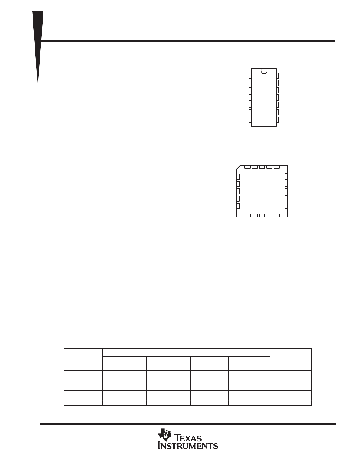
SN55109A, SN55110A ...J OR W PACKAGE
SN75109A, SN75110A, SN751 12...D OR N PACKAGE
(TOP VIEW)
1A
1
1B
2
1C
3
2C
4
2A
5
2B
6
GND
SN55109A, SN55110A . . . FK PACKAGE
1C
NC
2C
NC
2A
NC – No internal connection
7
(TOP VIEW)
1B1ANC2Z1Y
3 2 1 20 19
4
5
6
7
8
910111213
2B
GND
NC
14
13
12
11
10
9
8
CC+
V
2Y
18
17
16
15
14
V
1Y
1Z
V
D
2Z
2Y
CC+
CC –
1Z
NC
V
NC
D
CC –
These drivers feature independent channels with
common voltage supply and ground terminals.
RECOMMENDED FOR NEW DESIGNS
THE SN75109A IS NOT
The significant difference between the three
drivers is in the output current specification. The driver circuits feature a constant output current that is switched
to either of two output terminals by the appropriate logic levels at the input terminals. The output current can
be switched off (inhibited) by low logic levels on the enable inputs. The output current is nominally 6 mA for the
’109A, 12 mA for the ’110A, and 27 mA for the SN75112.
The enable/inhibit feature is provided so the circuits can be used in party-line or data-bus applications. A strobe
or inhibitor (enable D), common to both drivers, is included for increased driver-logic versatility. The output
current in the inhibited mode, I
, is specified so that minimum line loading is induced when the driver is used
O(off)
in a party-line system with other drivers. The output impedance of the driver in the inhibited mode is very high.
The output impedance of a transistor is biased to cutoff.
AVAILABLE OPTIONS
PACKAGED DEVICES
T
A
0°C to 70°C
–55°C to 125°C
The D package is available taped and reeled. Add the suffix R to the device type, (e.g., SN75110ADR).
SMALL OUTLINE
(D)
SN75109AD SN75109AN
SN75110AD
SN75112D SN75112N
CHIP CARRIER
(FK)
CERAMIC DIP
(J)
PLASTIC DIP
(N)
SN75110AN
CERAMIC
FLATPACK
(W)
PRODUCTION DATA information is current as of publication date.
Products conform to specifications per the terms of Texas Instruments
standard warranty. Production processing does not necessarily include
testing of all parameters.
POST OFFICE BOX 655303 • DALLAS, TEXAS 75265
Copyright 1995, Texas Instruments Incorporated
2–1
SN55109A, SN55110A
SN75109A, SN75110A, SN75112
DUAL LINE DRIVERS
SLLS106B – DECEMBER 1975 – REVISED MAY 1995
description (continued)
The driver outputs have a common-mode voltage range of –3 V to 10 V, allowing common-mode voltage on
the line without affecting driver performance.
All inputs are diode clamped and are designed to satisfy TTL-system requirements. The inputs are tested at
2 V for high-logic-level input conditions and 0.8 V for low-logic-level input conditions. These tests ensure
400-mV noise margin when interfaced with TTL Series 54/74.
The SN55109A and SN551 10A are characterized for operation over the full military temperature range of – 55°C
to 125°C. The SN75109A, SN75110A, and SN75112 are characterized for operation from 0°C to 70°C.
FUNCTION TABLE
(each driver)
LOGIC
INPUTS
A B C D Y Z
X X L X Off Off
X XXLOffOff
L XHHOnOff
X LHHOnOff
H H H H Off On
H = high level, L = low level, X = irrelevant
†
When using only one channel of the line drivers, the other
channel should be inhibited and/or have its outputs
grounded.
ENABLE
INPUTS
OUTPUTS
†
2–2
POST OFFICE BOX 655303 • DALLAS, TEXAS 75265
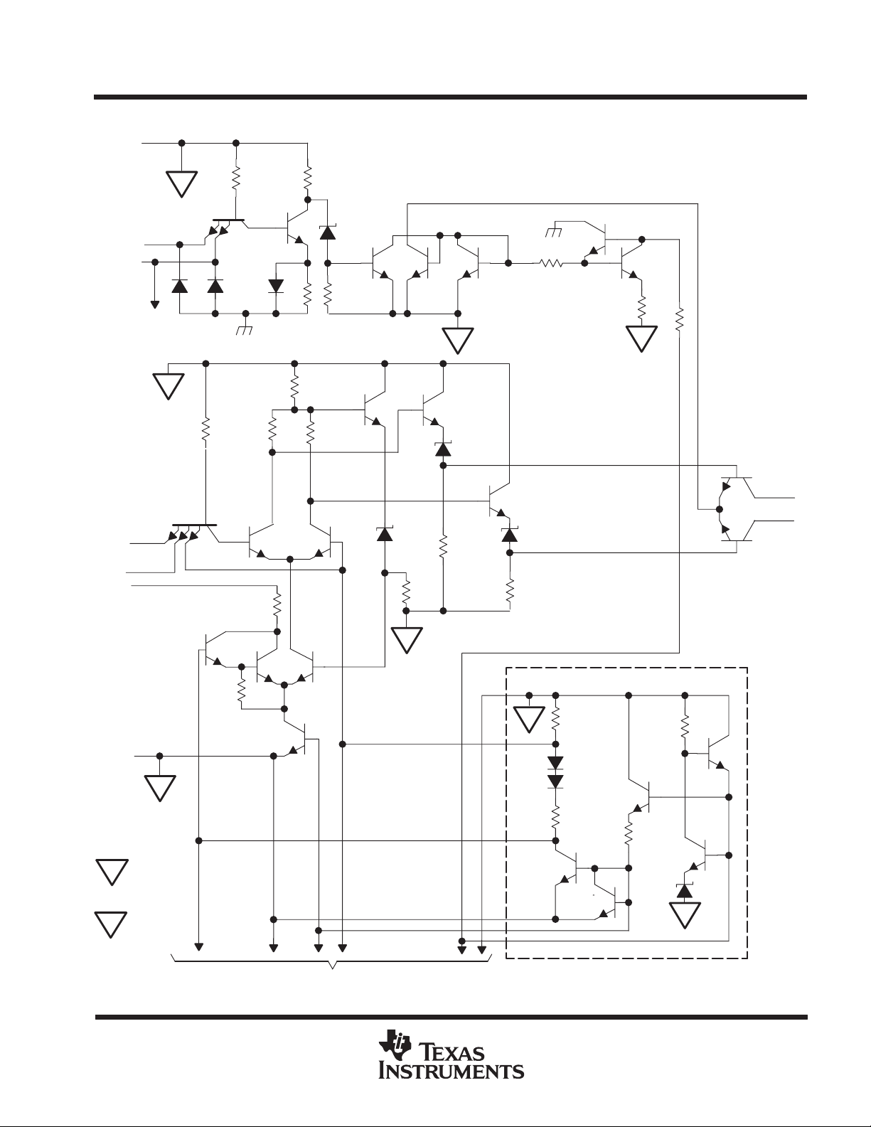
schematic (each driver)
14
V
CC+
SN55109A, SN55110A
SN75109A, SN75110A, SN75112
DUAL LINE DRIVERS
SLLS106B – DECEMBER 1975 – REVISED MAY 1995
GND
C
D
To Other
1, 5
A
2, 6
B
7
3, 4
10
Driver
2.2 kΩ
+
+
NOM
2.2 kΩ
NOM
–
–
8, 13
Y
9, 12
Z
11
V
CC–
–
+
... V
–
... V
Pin numbers shown are for D, J, N, and W packages.
CC+
CC–
bus
bus
To Other Driver
–
Common to Both Drivers
+
–
POST OFFICE BOX 655303 • DALLAS, TEXAS 75265
2–3
SN55109A, SN55110A
SN55109A
SN75109A
SN55110A
UNIT
SN75109A, SN75110A, SN75112
DUAL LINE DRIVERS
SLLS106B – DECEMBER 1975 – REVISED MAY 1995
absolute maximum ratings over operating free-air temperature range (unless otherwise noted)
SN55109A
SN55110A
Supply voltage, V
Supply voltage, V
Input voltage, VI 5.5 5.5 5.5 V
Output voltage range, V
Continuous total power dissipation (see Note 2) See Dissipation Rating Table
Operating free-air temperature range, T
Storage temperature range, T
Case temperature for 60 seconds: FK package 260 °C
Lead temperature 1,6 mm (1/16 inch) from case for 60 seconds J or W package 300 °C
Lead temperature 1,6 mm (1/16 inch) from case for 10 seconds D or N package 260 260 °C
†
Stresses beyond those listed under “absolute maximum ratings” may cause permanent damage to the device. These are stress ratings only, and
functional operation of the device at these or any other conditions beyond those indicated under “recommended operating conditions” is not
implied. Exposure to absolute-maximum-rated conditions for extended periods may affect device reliability.
NOTES: 1. Voltage values are with respect to network ground terminal.
2. In the FK, J, or W package, SN55109A and SN55110A chips are either silver glass or alloy mounted, and SN75109A, SN75110A,
and SN75112 chips are glass mounted.
(see Note 1) 7 7 7 V
CC+
CC–
O
A
stg
DISSIPATION RATING TABLE
PACKAGE
D 950 mW 7.6 mW/°C 608 mW —
FK 1375 mW 11.0 mW/°C 880 mW 275 mW
J 1375 mW 11.0 mW/°C 880 mW 275 mW
N 1150 mW 9.2 mW/°C 736 mW —
W 1000 mW 8.0 mW/°C 640 mW 200 mW
TA ≤ 25°C
POWER RATING
DERATING FACTOR
ABOVE TA = 25°C
POWER RATING
–7 –7 –7 V
–5 to 12 –5 to 12 –5 to 12 V
–55 to 125 0 to 70 0 to 70 °C
–65 to 150 –65 to 150 –65 to 150 °C
TA = 70°C
SN75109A
SN75110A
TA = 125°C
POWER RATING
SN75112 UNIT
†
recommended operating conditions (see Note 3)
SN75109A
MIN NOM MAX MIN NOM MAX
Supply voltage, VCC+ 4.5 5 5.5 4.75 5 5.25 V
Supply voltage, V
Positive common-mode output voltage 0 10 0 10 V
Negative common-mode output voltage 0 –3 0 –3 V
High-level input voltage, V
Low-level output current, V
Operating free-air temperature, T
NOTE 3: When using only one channel of the line drivers, the other channel should be inhibited and/or have its outputs grounded.
CC–
IH
IL
A
–4.5 –5 –5.5 –4.75 –5 –5.25 V
2 2 V
0.8 0.8 V
–55 125 0 70 °C
SN75110A
SN75112
2–4
POST OFFICE BOX 655303 • DALLAS, TEXAS 75265

SN55109A, SN55110A
†
SN75112
†
SN75112
I
O( )
On state out
ut current
V
O
1Vto1V
24
28
32
mA
I
On
state
o
tp
t
c
rrent
V
1
V
t
1
V
24
28
32
mA
I
I
V
CC±
= MAX V
I
=55V
mA
I
V
MAX
V
5
5
V
mA
IIHHigh level in
ut current
V
CC±
= MAX V
I
=24V
µA
IIHHigh
le
el
inp
t
c
rrent
V
MAX
V
2
4
V
A
IILLow level in
ut current
V
CC±
= MAX V
I
=04V
mA
IILLo
le
el
inp
t
c
rrent
V
MAX
V
0
4
V
mA
AandBin
uts at 0 4 V
mA
I
CC ( )
Su
ly current from V
CC
with driver enabled
A
and
B
in uts
at
0
4
V
C and D inputs at 2 V
18
30
345065
100
mA
I
S
ppl
c
rrent
from
V
ith
dri
er
enabled
C
d
D
i
t
t
2
V
18–30
34–50–65
100
mA
CC±
mA
SN75109A, SN75110A, SN75112
SLLS106B – DECEMBR 1975 – REVISED MAY 1995
DUAL LINE DRIVERS
SN55109A SN55110A
UNIT
SN75109A SN75110A
MAX
‡
MAX MIN TYP
‡
MAX MIN TYP
‡
MIN TYP
µ
–
–
1 1 1
2 2 2
40 40 40
80 80 80
–3 –3 –3
–6 –6 –6
18 30 23 35 25 40
18 21 30
–
–10 –17 –32
= 10 V 6 7 12 15 27 36
= –12 mA –0.9 –1.5 –0.9 –1.5 –0.9 –1.5 V
O
L
= MIN, I
= MAX, V
CC±
CC±
V
Input clamp voltage V
IK
V
= MIN to MAX,
CC
V
TEST CONDITIONS
PARAMETER
electrical characteristics over recommended operating free-air temperature range (unless otherwise noted)
,
o
= –
= 25°C
O
T
u
u
p
u
-
O(on)
= –3 V 3.5 6 6.5 12 18 27
O
= MIN, V
CC±
A
V
.
= 10 V 100 100 100 µA
=
O
I
,
=
= MIN, V
CC±
CC±
A, B, or C inputs
A, B, or C inputs
D input
Off-state output current V
Input current at maximum
input voltage
I
O(off)
I
POST OFFICE BOX 655303 DALLAS, TEXAS 75265
.
.
=
=
I
,
,
=
=
CC±
D input
A, B, or C inputs
u
u
u
u
p
p
v
v
w-
,
.
I
CC±
D input
s a
p
npu
= MAX,
an
CC±
V
v
with driver enabled
w
CC+
CC–
u
y
pp
u
Supply current from V
–(on)
+(on)
CC
CC
I
• 2–5
= MAX,
CC±
V
A, B, C, and D inputs at 0.4 V
= 25°C.
A
= –5 V, T
with driver inhibited
with driver inhibited
CC–
CC–
CC±
= 5 V, V
CC+
Supply current from V
Supply current from V
+(off)
–(off)
CC
CC
For conditions shown as MIN or MAX, use appropriate value specified under recommended operating conditions.
I
All typical values are at V
I
†
‡

SN55109A, SN55110A
PARAMETER
†
TEST CONDITIONS
MIN
TYP
MAX
UNIT
A or B
Y or Z
C
40 pF
R
50 Ω
See Figure 1
C or D
Y or Z
SN75109A, SN75110A, SN75112
DUAL LINE DRIVERS
SLLS106B – DECEMBER 1975 – REVISED MAY 1995
switching characteristics, V
FROM TO
(INPUT) (OUTPUT)
t
PLH
t
PHL
t
PLH
t
†
PHL
t
= Propagation delay time, low-to-high-level output
PLH
t
= Propagation delay time, high-to-low-level output
PHL
PARAMETER MEASUREMENT INFORMATION
Input A or B
50 Ω
Pulse
Generator
See Note A
Pulse
Generator
Input C or D
50%
Input A or B
Enable C or D
Output Y
t
PLH
t
w1
50% 50%
CC±
50 Ω
50%
= ±5 V, T
t
PHL
= 25°C
A
p
=
L
VCC
+
To Other Driver
See Note C
TEST CIRCUIT
,
L
VCC
,
=
–
890 Ω
RL = 50 Ω
t
w2
50% 50%
t
PLH
50% 50%
890 Ω
9 15 ns
9 15 ns
16 25 ns
13 25 ns
RL = 50 Ω
Output Y
CL = 40 pF
(see Note B)
Output Z
CL = 40 pF
(see Note B)
0 V
t
PHL
off
3 V
0 V
3 V
on
t
PHL
Output Z
50% 50%
NOTES: A. The pulse generators have the following characteristics: ZO = 50 Ω, tr = tf = 10 ± 5 ns, tw1 = 500 ns, PRR ≤ 1 MHz, tw2 = 1 µs,
PRR ≤ 500 kHz.
B. CL includes probe and jig capacitance.
C. For simplicity, only one channel and the enable connections are shown.
t
PLH
VOLTAGE WAVEFORMS
Figure 1. Test Circuit and Voltage Waveforms
2–6
POST OFFICE BOX 655303 • DALLAS, TEXAS 75265
off
on

TYPICAL CHARACTERISTICS
SN55109A, SN55110A
SN75109A, SN75110A, SN75112
DUAL LINE DRIVERS
SLLS106B – DECEMBER 1975 – REVISED MAY 1995
SN55109A, SN75109A
ON-STATE OUTPUT CURRENT
vs
NEGATIVE SUPPLY VOLTAGE
7
V
= 4.5 V
CC+
VO = –3 V
6
TA = 25°C
5
4
3
2
1
O(on)
IO(on) – On-State Output Current – mA
I
0
–3
–4 –5 –6
V
– Negative Supply Voltage – V
CC–
Figure 2 Figure 3
–7
SN55110A, SN75110A
ON-STATE OUTPUT CURRENT
vs
NEGATIVE SUPPLY VOLTAGE
14
V
= 4.5 V
CC+
VO = –3 V
12
TA = 25°C
10
8
6
4
O(on)
IO(on) – On-State Output Current – mA
I
2
0
–3 –7–4 –5 –6
V
– Negative Supply Voltage – V
CC–
SN75112
ON-STATE OUTPUT CURRENT
vs
NEGATIVE SUPPLY VOLTAGE
35
V
= 4.5 V
CC+
VO = –3 V
30
TA = 25°C
25
20
15
10
O(on)
5
IO(on) – On-State Output Current – mA
I
0
–3
–4 –5 –6
V
– Negative Supply Voltage – V
CC–
Figure 4
–7
POST OFFICE BOX 655303 • DALLAS, TEXAS 75265
2–7

SN55109A, SN55110A
SN75109A, SN75110A, SN75112
DUAL LINE DRIVERS
SLLS106B – DECEMBER 1975 – REVISED MAY 1995
APPLICATION INFORMATION
special pulse-control circuit
Figure 5 shows a circuit that may be used as a pulse generator output or in many other testing applications.
INPUT OUTPUTS
AYZ
High
Low
Input
2.5 V
OffOnOn
Off
5 V
3
2
V
CC+
A
B
Y
Z
1
4
5
1
6
3
2
4
6
5
To Other Logic and
Strobe Inputs
Input Pulse
Switch
Position
Output Pulse
C
D
1/2 ‘109A
‘110A,
GND
0 V
123 456
or SN75112
V
CC–
–5 V
3
2
1
4
5
6
Output
0 V
Figure 5. Pulse-Control Circuit
2–8
POST OFFICE BOX 655303 • DALLAS, TEXAS 75265

SN55109A, SN55110A
SN75109A, SN75110A, SN75112
DUAL LINE DRIVERS
SLLS106B – DECEMBER 1975 – REVISED MAY 1995
APPLICATION INFORMATION
using the SN75112 as a CCITT recommended V.35 line driver
The SN75112 dual line driver, the SN75107A dual line receiver, and some external resistors can be used to
implement the data interchange circuit of CCITT recommendation V .35 (1976) modem specification. The circuit
of one channel is shown in Figure 1 and meets the requirement of the interface as specified by Appendix 1 1 of
CCITT V.35 and summarized in Table 1 (V.35 has been replaced by ITU V.11).
Table 1. CCITT V.35 Electrical Requirements
MIN MAX UNIT
GENERATOR
Source impedance, Z
Resistance to ground, R 135 165 Ω
Differential output voltage, V
10% to 90% rise time, t
or 0.01 × ui
Common-mode output voltage, V
LOAD (RECEIVER)
Input impedance, Z
Resistance to ground, R 135 165 Ω
†
ui = unit interval or minimum signal element pulse width
source
OD
r
OC
I
50 150 Ω
440 660 mV
40 ns
†
– 0.6 0.6 V
90 110 Ω
5 V
1/2 SN75112
1A
1
Data In
Enable
All resistors are 5%, 1/4 W.
2
1B
10
3
1C
Figure 6. CCITT Recommended V.35 Interface Using the SN75112 and SN75107A
R4
390 Ω
13
12
5 V
5 V
R3
390 Ω
100 pF
1 Y
1 Z
100 pF
R1
1.3 kΩ
R5
75 Ω
R2
1.3 kΩ
R6
50 Ω
R7
50 Ω
R8
125 Ω
1A
1
2
1B
5 V
Strobe
6
1/2 SN75107A
4
1Y
Data Out
5
1G
Enable
POST OFFICE BOX 655303 • DALLAS, TEXAS 75265
2–9

SN55109A, SN55110A
SN75109A, SN75110A, SN75112
DUAL LINE DRIVERS
SLLS106B – DECEMBER 1975 – REVISED MAY 1995
2–10
POST OFFICE BOX 655303 • DALLAS, TEXAS 75265

IMPORTANT NOTICE
T exas Instruments (TI) reserves the right to make changes to its products or to discontinue any semiconductor
product or service without notice, and advises its customers to obtain the latest version of relevant information
to verify, before placing orders, that the information being relied on is current and complete.
TI warrants performance of its semiconductor products and related software to the specifications applicable at
the time of sale in accordance with TI’s standard warranty. Testing and other quality control techniques are
utilized to the extent TI deems necessary to support this warranty. Specific testing of all parameters of each
device is not necessarily performed, except those mandated by government requirements.
Certain applications using semiconductor products may involve potential risks of death, personal injury, or
severe property or environmental damage (“Critical Applications”).
TI SEMICONDUCTOR PRODUCTS ARE NOT DESIGNED, INTENDED, AUTHORIZED, OR WARRANTED
TO BE SUITABLE FOR USE IN LIFE-SUPPORT APPLICATIONS, DEVICES OR SYSTEMS OR OTHER
CRITICAL APPLICATIONS.
Inclusion of TI products in such applications is understood to be fully at the risk of the customer. Use of TI
products in such applications requires the written approval of an appropriate TI officer . Questions concerning
potential risk applications should be directed to TI through a local SC sales office.
In order to minimize risks associated with the customer’s applications, adequate design and operating
safeguards should be provided by the customer to minimize inherent or procedural hazards.
TI assumes no liability for applications assistance, customer product design, software performance, or
infringement of patents or services described herein. Nor does TI warrant or represent that any license, either
express or implied, is granted under any patent right, copyright, mask work right, or other intellectual property
right of TI covering or relating to any combination, machine, or process in which such semiconductor products
or services might be or are used.
Copyright 1998, Texas Instruments Incorporated

Copyright © Each Manufacturing Company.
All Datasheets cannot be modified without permission.
This datasheet has been download from :
www.AllDataSheet.com
100% Free DataSheet Search Site.
Free Download.
No Register.
Fast Search System.
www.AllDataSheet.com
 Loading...