

查询SN74V3640-15PEU供应商
D
Choice of Memory Organizations
– SN74V3640 – 1024 × 36 Bit
– SN74V3650 – 2048 × 36 Bit
– SN74V3660 – 4096 × 36 Bit
– SN74V3670 – 8192 × 36 Bit
– SN74V3680 – 16384 × 36 Bit
– SN74V3690 – 32768 × 36 Bit
D
166-MHz Operation (6-ns Read/Write Cycle
Time)
D
User-Selectable Input- and Output-Port Bus
Sizing
– ×36 in to ×36 out
– ×36 in to ×18 out
– ×36 in to ×9 out
– ×18 in to ×36 out
– ×9 in to ×36 out
D
Big-Endian/Little-Endian User-Selectable
Byte Representation
D
5-V-Tolerant Inputs
D
Fixed, Low, First-Word Latency
D
Zero-Latency Retransmit
D
Master Reset Clears Entire FIFO
D
Partial Reset Clears Data, But Retains
Programmable Settings
SN74V3640, SN74V3650, SN74V3660, SN74V3670, SN74V3680, SN74V3690
1024 × 36, 2048 × 36, 4096 × 36, 8192 × 36, 16384 × 36, 32768 × 36
3.3-V CMOS FIRST-IN, FIRST-OUT MEMORIES
SCAS668A – NOVEMBER 2001 – REVISED MARCH 2003
D
Empty, Full, and Half-Full Flags Signal FIFO
Status
D
Programmable Almost-Empty and
Almost-Full Flags; Each Flag Can Default to
One of Eight Preselected Offsets
D
Selectable Synchronous/Asynchronous
Timing Modes for Almost-Empty and
Almost-Full Flags
D
Program Programmable Flags by Either
Serial or Parallel Means
D
Select Standard Timing (Using EF and FF
Flags) or First-Word Fall-Through (FWFT)
Timing (Using OR
D
Output Enable Puts Data Outputs in
High-Impedance State
D
Easily Expandable in Depth and Width
D
Independent Read and Write Clocks Permit
Reading and Writing Simultaneously
D
High-Performance Submicron CMOS
Technology
D
Available in 128-Pin Thin Quad Flat Pack
(TQFP)
and IR Flags)
description
The SN74V3640, SN74V3650, SN74V3660, SN74V3670, SN74V3680, and SN74V3690 are exceptionally
deep, high-speed CMOS, first-in first-out (FIFO) memories, with clocked read and write controls and a flexible
bus-matching ×36/×18/×9 data flow. These FIFOs offer several key user benefits:
D
Flexible ×36/×18/×9 bus matching on both read and write ports
D
The period required by the retransmit operation is fixed and short.
D
The first-word data-latency period, from the time the first word is written to an empty FIFO to the time it can
be read, is fixed and short.
D
High-density offerings up to 1 Mbit
Bus-matching synchronous FIFOs are particularly appropriate for network, video, signal processing,
telecommunications, data communications, and other applications that need to buffer large amounts of data
and match buses of unequal sizes.
Each FIFO has a data input port (Dn) and a data output port (Qn), both of which can assume 36-bit, 18-bit, or
9-bit width, as determined by the state of external control pins’ input width (IW), output width (OW), and bus
matching (BM) during the master-reset cycle.
Please be aware that an important notice concerning availability, standard warranty, and use in critical applications of
Texas Instruments semiconductor products and disclaimers thereto appears at the end of this data sheet.
PRODUCTION DATA information is current as of publication date.
Products conform to specifications per the terms of Texas Instruments
standard warranty. Production processing does not necessarily include
testing of all parameters.
POST OFFICE BOX 655303 • DALLAS, TEXAS 75265
Copyright 2003, Texas Instruments Incorporated
1
SN74V3640, SN74V3650, SN74V3660, SN74V3670, SN74V3680, SN74V3690
1024 × 36, 2048 × 36, 4096 × 36, 8192 × 36, 16384 × 36, 32768 × 36
3.3-V CMOS FIRST-IN, FIRST-OUT MEMORIES
SCAS668A – NOVEMBER 2001 – REVISED MARCH 2003
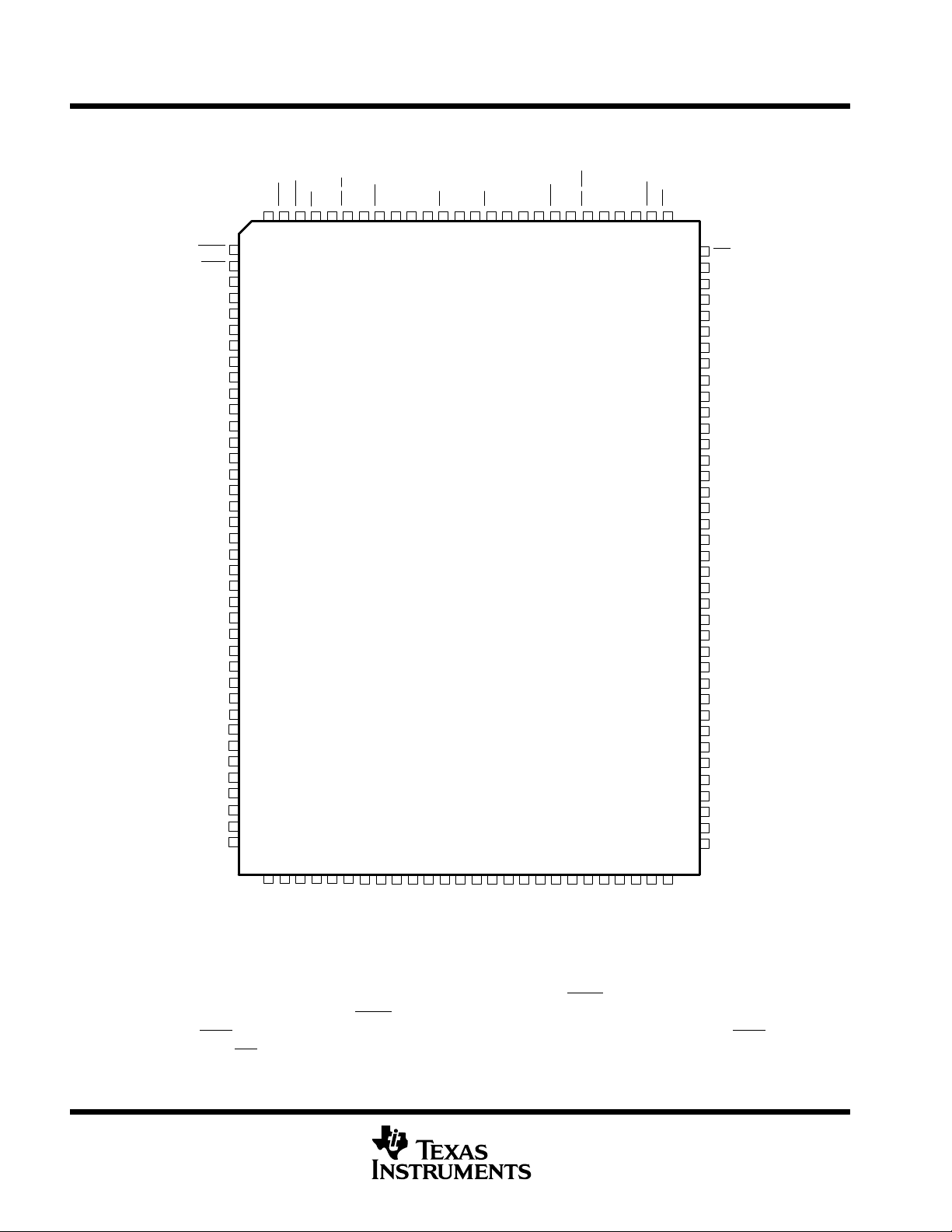
PEU PACKAGE
(TOP VIEW)
WEN
SEN
DNC
V
CC
DNC
IW
D35
D34
D33
D32
V
CC
D31
D30
GND
D29
D28
D27
D26
D25
D24
D23
GND
D22
V
CC
D21
D20
D19
D18
GND
D17
D16
D15
D14
D13
V
CC
D12
GND
D11
1
2
3
4
5
6
7
8
9
10
11
12
13
14
15
16
17
18
19
20
21
22
23
24
25
26
27
28
29
30
31
32
33
34
35
36
37
38
PRS
WCLK
127
128
40
39
MRS
126
41
FWFT/SI
LD
124
125
43
42
V
FF/IR
122
123
44
CC
45
PAF
121
46
GND
120
47
OW
119
48
HF
FSEL0
117
118
50
49
GND
116
51
FSEL1
BE
114
115
53
52
CC
V
IP
BM
PAE
111
110
112
113
57
56
55
54
PFM
109
58
RM
EF/OR
107
108
60
59
GND
106
61
RCLK
REN
104
105
63
62
RT
103
102
101
100
99
98
97
96
95
94
93
92
91
90
89
88
87
86
85
84
83
82
81
80
79
78
77
76
75
74
73
72
71
70
69
68
67
66
65
64
OE
V
CC
V
CC
Q35
Q34
Q33
Q32
GND
GND
Q31
Q30
Q29
Q28
Q27
Q26
V
CC
Q25
Q24
GND
GND
Q23
Q22
Q21
Q20
Q19
Q18
GND
Q17
Q16
V
CC
V
CC
Q15
Q14
Q13
Q12
GND
Q11
Q10
D9
D7
D6
D10
D8
D5D4D3
GND
V
CC
D2D1D0
GND
Q0
Q1
Q2
Q3Q4Q5
GND
Q6
V
CC
Q7
Q8
Q9
DNC = Do not connect
description (continued)
The input port is controlled by write-clock (WCLK) and write-enable (WEN) inputs. Data is written into the FIFO
on every rising edge of WCLK when WEN
read-enable (REN
An output-enable (OE
2
) inputs. Data is read from the FIFO on every rising edge of RCLK when REN is asserted.
) input is provided for 3-state control of the outputs.
POST OFFICE BOX 655303 • DALLAS, TEXAS 75265
is asserted. The output port is controlled by read-clock (RCLK) and
SN74V3640, SN74V3650, SN74V3660, SN74V3670, SN74V3680, SN74V3690
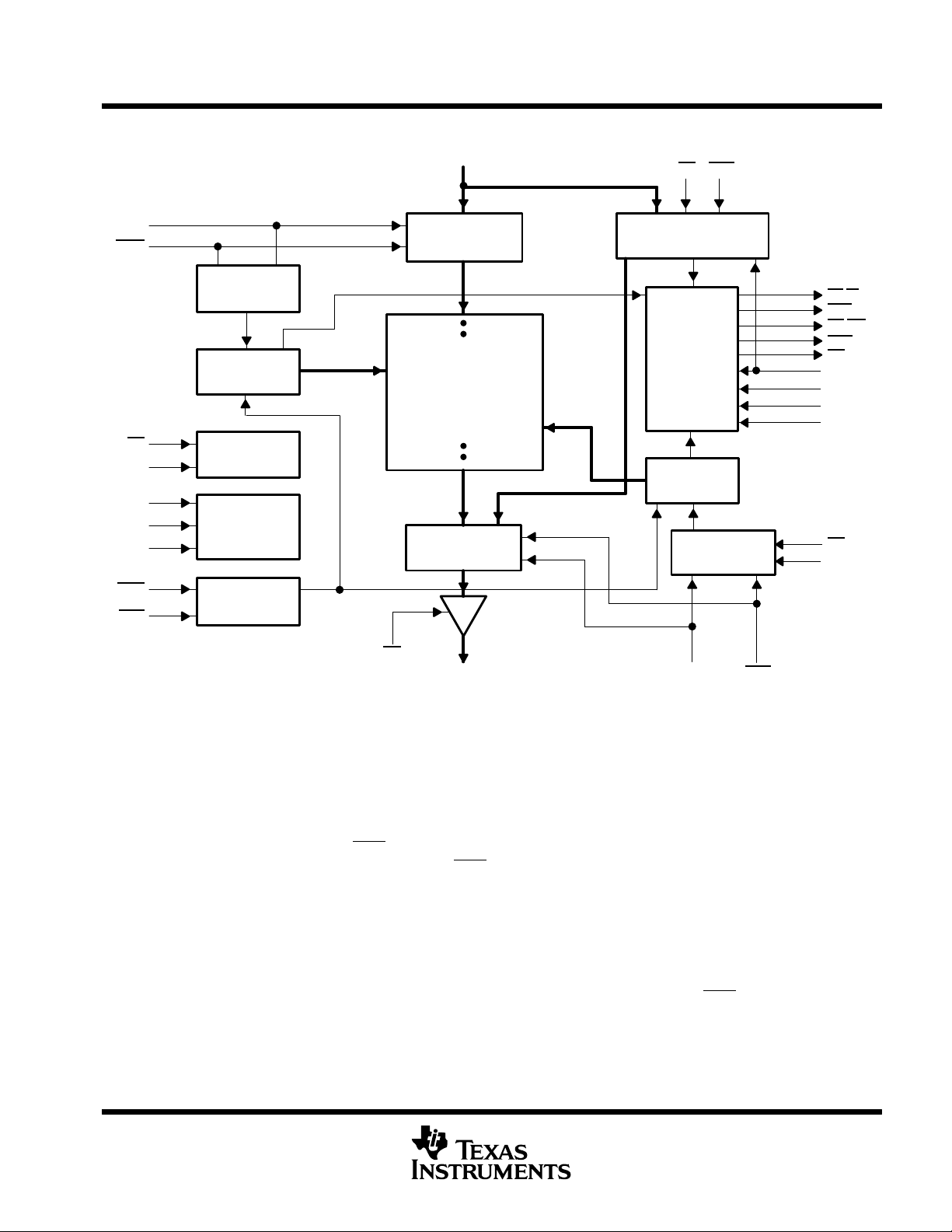
functional block diagram
1024 × 36, 2048 × 36, 4096 × 36, 8192 × 36, 16384 × 36, 32768 × 36
3.3-V CMOS FIRST-IN, FIRST-OUT MEMORIES
SCAS668A – NOVEMBER 2001 – REVISED MARCH 2003
WCLK
WEN
BE
BM
IW
OW
MRS
PRS
D0–Dn (×36, ×18, or ×9)
128
1
Write-Control
Logic
Write
Pointer
16384 × 36, 32768 × 36
114
113
IP
112
6
119
126
127
Control
Logic
Bus
Configuration
Reset
Logic
102
OE
Q0–Qn (×36, ×18, or ×9)
Input
Register
RAM Array
1024 × 36, 2048 × 36,
4096 × 36, 8192 × 36,
Output
Register
SEN
LD
125
Offset
Register
Flag
Logic
Read
Pointer
Read-Control
Logic
105 104
2
123
FF/IR
121
PAF
108
EF/OR
110
PAE
117
HF
124
FWFT/SI
109
PFM
118
FSEL0
115
FSEL1
103
RT
107
RM
RENRCLK
description (continued)
The frequencies of the RCLK and WCLK signals can vary from 0 to f
are no restrictions on the frequency of one clock input with respect to the other.
There are two possible timing modes of operation with these devices: first-word fall-through (FWFT) mode and
standard mode.
In FWFT mode, the first word written to an empty FIFO is clocked directly to the data output lines after three
transitions of the RCLK signal. REN need not be asserted for accessing the first word. However, subsequent
words written to the FIFO do require a low on REN
for access. The state of the FWFT/SI input during master
reset determines the timing mode.
For applications requiring more data-storage capacity than a single FIFO can provide, the FWFT timing mode
permits depth expansion by chaining FIFOs in series (i.e., the data outputs of one FIFO are connected to the
corresponding data inputs of the next). No external logic is required.
In standard mode, the first word written to an empty FIFO does not appear on the data output lines unless a
specific read operation is performed. A read operation, which consists of activating REN
RCLK edge, shifts the word from internal memory to the data output lines.
, with complete independence. There
MAX
and enabling a rising
POST OFFICE BOX 655303 • DALLAS, TEXAS 75265
3
SN74V3640, SN74V3650, SN74V3660, SN74V3670, SN74V3680, SN74V3690
1024 × 36, 2048 × 36, 4096 × 36, 8192 × 36, 16384 × 36, 32768 × 36
3.3-V CMOS FIRST-IN, FIRST-OUT MEMORIES
SCAS668A – NOVEMBER 2001 – REVISED MARCH 2003
Partial Reset (PRS)
Write Clock (WCLK)
Write Enable (WEN
Load (LD
(×36, ×18, ×9) Data In (D0–Dn)
Serial Enable (SEN
First-Word Fall-Through or Serial Input
Full Flag or Input Ready (FF
Programmable Almost-Full Flag (PAF
(FWFT/SI)
/IR)
Input Width (IW)
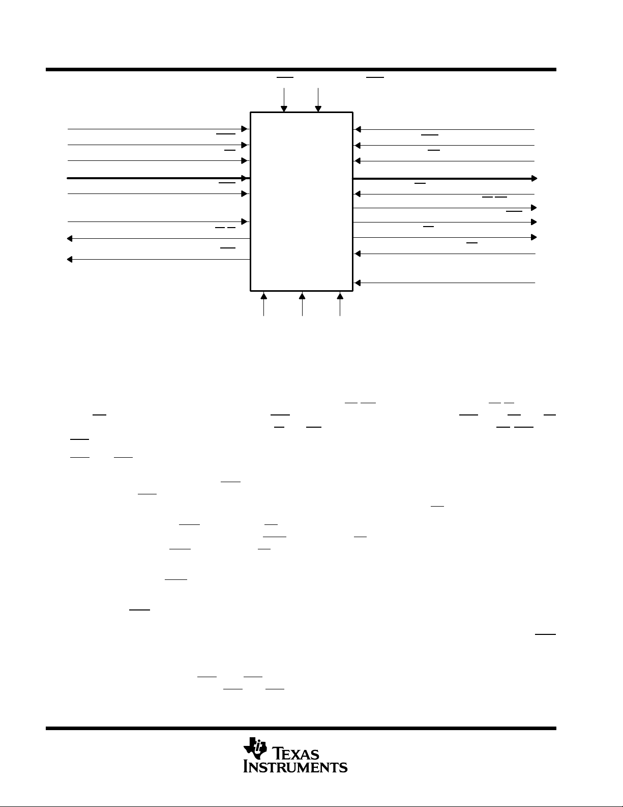
Figure 1. Single-Device-Configuration Signal Flow
Master Reset (MRS)
Read Clock (RCLK)
)
)
SN74V3640
)
)
SN74V3650
SN74V3660
SN74V3670
SN74V3680
SN74V3690
Bus
Matching
(BM)
Output Width (OW)
Read Enable (REN)
Output Enable (OE
(×36, ×18, ×9) Data Out (Q0–Qn)
Retransmit (RT
Empty Flag or Output Ready (EF/OR)
Programmable Almost-Empty Flag (PAE
Half-Full Flag (HF
Big Endian/Little Endian (BE
Interspersed/
Noninterspersed Parity (IP)
)
)
)
)
)
description (continued)
These FIFOs have five flag pins: empty flag or output ready (EF/OR), full flag or input ready (FF/IR), half-full
flag (HF
functions are selected in standard mode. The IR and OR functions are selected in FWFT mode. HF, PAE, and
PAF
PAE
determine the flag-switching threshold and can be loaded by parallel or serial methods. Eight default offset
settings also are provided, so that P AE
boundary. The PAF
offset values are set during master reset by the state of the FSEL0, FSEL1, and LD
For serial programming, SEN
edge of WCLK. For parallel programming, WEN
rising edge of WCLK. REN
RCLK, regardless of whether serial parallel offset loading has been selected.
During master reset (MRS
selects standard mode or FWFT mode.
Partial reset (PRS
mode, programmable-flag programming method, and default or programmed offset settings existing before
partial reset remain unchanged. The flags are updated according to the timing mode and offsets in effect. PRS
is useful for resetting a device in mid-operation, when reprogramming programmable flags would be
undesirable.
Also, the timing modes of PAE
asynchronous or synchronous for PAE
), programmable almost-empty flag (PAE), and programmable almost-full flag (PAF). The EF and FF
always are available for use, regardless of timing mode.
and PAF can be programmed independently to switch at any point in memory. Programmable offsets
can be set to switch at a predefined number of locations from the empty
threshold also can be set at similar predefined values from the full boundary. The default
.
, together with LD, loads the offset registers via the serial input (SI) on each rising
, together with LD, loads the offset registers via Dn on each
, together with LD, can read the offsets in parallel from Qn on each rising edge of
), the read and write pointers are set to the first location of the FIFO. The FWFT pin
) also sets the read and write pointers to the first location of the memory . However, the timing
and PAF outputs can be selected. Timing modes can be set as either
and PAF.
4
POST OFFICE BOX 655303 • DALLAS, TEXAS 75265
SN74V3640, SN74V3650, SN74V3660, SN74V3670, SN74V3680, SN74V3690
1024 × 36, 2048 × 36, 4096 × 36, 8192 × 36, 16384 × 36, 32768 × 36
3.3-V CMOS FIRST-IN, FIRST-OUT MEMORIES
SCAS668A – NOVEMBER 2001 – REVISED MARCH 2003
description (continued)
If the asynchronous PAE/PAF configuration is selected, PAE is asserted low on the low-to-high transition of
RCLK. PAE
low-to-high transition of WCLK, and PAF
If the synchronous P AE/PAF configuration is selected , the PAE is asserted and updated on the rising edge of
RCLK only, and not WCLK. Similarly, PAF
RCLK. The mode desired is configured during master reset by the state of the programmable flag mode (PFM).
is reset to high on the low-to-high transition of WCLK. Similarly, PAF is asserted low on the
is reset to high on the low-to-high transition of RCLK.
is asserted and updated on the rising edge of WCLK only, and not
The retransmit function allows data to be reread from the FIFO more than once. A low on the retransmit (RT
input during a rising RCLK edge initiates a retransmit operation by setting the read pointer to the first location
of the memory array. Zero-latency retransmit timing mode can be selected using the retransmit timing mode
(RM). During master reset, a low on RM selects zero-latency retransmit. A high on RM during master reset
selects normal latency.
If zero-latency retransmit operation is selected, the first data word to be retransmitted is placed on the output
register, with respect to the same RCLK edge that initiated the retransmit, if RT
is low.
See Figures 1 1 and 12 for normal latency retransmit timing. See Figures 13 and 14 for zero-latency retransmit
timing.
The devices can be configured with different input and output bus widths (see Table 1).
Table 1. Bus-Matching Configuration Modes
BM IW OW
L L L ×36 ×36
H L L ×36 ×18
H L H ×36 ×9
H H L ×18 ×36
H H H ×9 ×36
†
Logic levels during master reset
WRITE-PORT
WIDTH
READ-PORT
WIDTH
†
A big-endian/little-endian data word format is provided. This function is useful when data is written into the FIFO
in long-word (×36/×18) format and read out of the FIFO in small-word (×18/×9) format. If big-endian mode is
selected, the most-significant byte (MSB) (word) of the long word written into the FIFO is read out of the FIFO
first, followed by the least-significant byte (LSB). If little-endian format is selected, the LSB of the long word
written into the FIFO is read out first, followed by the MSB. The mode desired is configured during master reset
by the state of the big-endian/little-endian (BE
) pin (see Figure 4 for the bus-matching byte arrangement).
)
The interspersed/noninterspersed parity (IP) bit function allows the user to select the parity bit in the word loaded
into the parallel port (D0–Dn) when programming the flag offsets. If interspersed-parity mode is selected, the
FIFO assumes that the parity bit is located in bit positions D8, D17, D26, and D35 during the parallel
programming of the flag offsets. If noninterspersed-parity mode is selected, D8, D17, and D26 are assumed
to be valid bits, and D32, D33, D34, and D35 are ignored. Interspersed parity mode is selected during master
reset by the state of the IP input. Interspersed parity control has an effect only during parallel programming of
the offset registers. It does not affect data written to and read from the FIFO.
The SN74V3640, SN74V3650, SN74V3660, SN74V3670, SN74V3680, and SN74V3690 are fabricated using
high-speed submicron CMOS technology, and are characterized for operation from 0°C to 70°C.
POST OFFICE BOX 655303 • DALLAS, TEXAS 75265
5
SN74V3640, SN74V3650, SN74V3660, SN74V3670, SN74V3680, SN74V3690
1024 × 36, 2048 × 36, 4096 × 36, 8192 × 36, 16384 × 36, 32768 × 36
3.3-V CMOS FIRST-IN, FIRST-OUT MEMORIES
SCAS668A – NOVEMBER 2001 – REVISED MARCH 2003
Terminal Functions
TERMINAL
NAME
†
BE
†
BM
D0–D36 I
EF/OR O
FF/IR O
†
FSEL0
†
FSEL1
FWFT/SI I
HF O Half-full flag. HF indicates whether the FIFO memory is more or less than half full.
†
IP
†
IW
LD I
MRS I
OE I Output enable. OE controls the output impedance of Qn.
†
OW
PAE O
PAF O
†
PFM
PRS I
Q0–Q35 O
RCLK I
†
Inputs should not change state after master reset.
I/O DESCRIPTION
Big endian/little endian. During master reset, a low on BE selects big-endian operation. A high on BE during master
I
reset selects little-endian format.
Bus matching. BM works with IW and OW to select the bus sizes for both write and read ports (see T able 1 for bus-size
I
configuration).
Data inputs. Data inputs for a 36-, 18-, or 9-bit bus. When in 18- or 9-bit mode, the unused input pins are in a
don’t-care state.
Empty flag/output ready. In standard mode, the EF function is selected. EF indicates whether the FIFO memory is
empty. In FWFT mode, the OR
Full flag/input ready . In standard mode, the FF function is selected. FF indicates whether the FIFO memory is full. In
FWFT mode, the IR
Flag-select bit 0. During master reset, FSEL0, along with FSEL1 and LD, selects the default offset values for PAE and
I
PAF
. Up to eight possible settings are available.
Flag-select bit 1. During master reset, FSEL1, along with FSEL0 and LD, selects the default offset values for PAE and
I
PAF
. Up to eight possible settings are available.
First-word fall-through/serial in. During master reset, FWFT/SI selects FWFT or standard mode. After master reset,
FWFT/SI functions as a serial input for loading offset registers.
Interspersed parity. During master reset, a low on IP selects noninterspersed-parity mode. A high selects
interspersed-parity mode. Interspersed-parity control has an effect only during parallel programming of the offset
I
registers. It does not effect data written to and read from the FIFO.
I Input width. IW, along with OW and BM, selects the bus width of the write port (see Table 1 for bus-size configuration).
Load. This is a dual-purpose pin. During master reset, the state of LD, along with FSEL0 and FSEL1, determines one
of eight default offset values for PAE
programmed, parallel or serial (see Table 2). After master reset, LD
registers.
Master reset. MRS initializes the read and write pointers to zero and sets the output register to all zeroes. During
master reset, the FIFO is configured for either FWFT or standard mode, bus-matching configurations, one of eight
programmable-flag default settings, serial or parallel programming of the offset settings, big-endian/little-endian
format, zero-latency timing mode, interspersed parity, and synchronous versus asynchronous programmable-flag
timing modes.
I Output width. OW, along with IW and BM, selects the bus width of the read port (see T able 1 for bus-size configuration).
Programmable almost-empty flag. PAE goes low if the number of words in the FIFO memory is less than of fset n, which
is stored in the empty offset register. PAE
equal to, offset n.
Programmable almost-full flag. PAF goes high if the number of free locations in the FIFO memory is more than
offset m, which is stored in the full offset register. PAF
is less than, or equal to, m.
Programmable-flag mode. During master reset, a low on PFM selects asynchronous programmable-flag timing mode.
I
A high on PFM selects synchronous programmable-flag timing mode.
Partial reset. PRS initializes the read and write pointers to zero and sets the output register to all zeroes. During partial
reset, the existing mode (standard or FWFT), programming method (serial or parallel), and programmable-flag
settings are all retained.
Data outputs. Data outputs for a 36-, 18-, or 9-bit bus. When in 18- or 9-bit mode, the unused output pins are in a
don’t-care state. Outputs are not 5-V tolerant, regardless of the state of OE
Read clock. When enabled by REN, the rising edge of RCLK reads data from the FIFO memory and offsets from the
programmable registers.
function is selected. IR indicates whether there is space available for writing to the FIFO memory.
function is selected. OR indicates whether there is valid data available at the outputs.
and PAF, along with the method by which these offset registers can be
enables writing to and reading from the offset
goes high if the number of words in the FIFO memory is greater than, or
goes low if the number of free locations in the FIFO memory
.
6
POST OFFICE BOX 655303 • DALLAS, TEXAS 75265
SN74V3640, SN74V3650, SN74V3660, SN74V3670, SN74V3680, SN74V3690
1024 × 36, 2048 × 36, 4096 × 36, 8192 × 36, 16384 × 36, 32768 × 36
3.3-V CMOS FIRST-IN, FIRST-OUT MEMORIES
SCAS668A – NOVEMBER 2001 – REVISED MARCH 2003
Terminal Functions (Continued)
TERMINAL
NAME
REN I Read enable. REN enables RCLK for reading data from the FIFO memory and offset registers.
†
RM
RT I
SEN I Serial enable. SEN enables serial loading of programmable flag offsets.
WCLK I
WEN I Write enable. WEN enables WCLK for writing data into the FIFO memory and offset registers.
†
Inputs should not change state after master reset.
I/O DESCRIPTION
Retransmit latency mode. During master reset, a low on RM selects zero-latency retransmit timing mode. A high on
I
RM selects normal-latency mode.
Retransmit. RT asserted on the rising edge of RCLK initializes the READ pointer to zero, sets the EF flag to low (OR
to high in FWFT mode) and does not disturb the write pointer, programming method, existing timing mode, or
programmable-flag settings. RT
Write clock. When enabled by WEN, the rising edge of WCLK writes data into the FIFO and offsets into the
programmable registers for parallel programming and, when enabled by SEN
of data into the programmable register for serial programming.
is useful to reread data from the first physical location of the FIFO.
, the rising edge of WCLK writes one bit
detailed description
inputs
data in (D0–Dn)
D0–D35 are data inputs for 36-bit-wide data. D0–D17 are data inputs for 18-bit-wide data. D0–D8 are data
inputs for 9-bit-wide data.
controls
master reset (MRS
A master reset is accomplished when MRS
to the first location of the RAM array. PAE
)
is taken low. This operation sets the internal read and write pointers
goes low, PAF goes high, and HF goes high.
If FWFT/SI is low during master reset, the standard mode, EF
high. If FWFT/SI is high, the FWFT mode, IR
All control settings, such as OW, IW, BM, BE
, and OR are selected. OR goes high and IR goes low.
, RM, PFM, and IP are defined during the master reset cycle.
, and FF are selected. EF goes low and FF goes
During a master reset, the output register is initialized to all zeroes. A master reset is required after power up,
before a write operation can take place. MRS
is asynchronous.
See Figure 5 for timing information.
POST OFFICE BOX 655303 • DALLAS, TEXAS 75265
7

SN74V3640, SN74V3650, SN74V3660, SN74V3670, SN74V3680, SN74V3690
1024 × 36, 2048 × 36, 4096 × 36, 8192 × 36, 16384 × 36, 32768 × 36
3.3-V CMOS FIRST-IN, FIRST-OUT MEMORIES
SCAS668A – NOVEMBER 2001 – REVISED MARCH 2003
partial reset (PRS)
A partial reset is accomplished when the PRS
the internal read and write pointers are set to the first location of the RAM array , P AE
and HF
Whichever mode is active at the time of partial reset remains selected (standard or FWFT mode). If standard
mode is active, FF
Following partial reset, all values held in the offset registers remain unchanged. The programming method
(parallel or serial) active at the time of partial reset also is retained. The output register is initialized to all zeroes.
PRS
A partial reset is useful for resetting the device during operation when reprogramming programmable-flag
offsets might not be convenient.
See Figure 6 for timing information.
goes high.
goes high and EF goes low. If the FWFT mode is active, OR goes high and IR goes low.
is asynchronous.
input is taken to a low state. As in the case of the master reset,
goes low, PAF goes high,
retransmit (RT
The retransmit operation allows previously read data to be accessed again. There are two modes of retransmit
operation: normal latency and zero latency. There are two stages to retransmit. The first stage is a setup
procedure that resets the read pointer to the first location of memory . The second stage is the actual retransmit,
which consists of reading out the memory contents, starting at the beginning of the memory.
Retransmit setup is initiated by holding RT
bringing RT
If standard mode is selected, the FIFO marks the beginning of the retransmit setup by setting EF
change in level is noticeable only if EF
initialized to the first location of the RAM array.
When EF
in memory . Because standard mode is selected, every word read, including the first word following retransmit
setup, requires a low on REN
See Figure 11 for timing information.
If FWFT mode is selected, the FIFO marks the beginning of the retransmit setup by setting OR
period, the internal read pointer is set to the first location of the RAM array.
When OR
the outputs. Because FWFT mode is selected, the first word appears on the outputs and no low on REN
necessary. Reading all subsequent words requires a low on REN
See Figure 12 for timing information.
)
low during a rising RCLK edge. REN and WEN must be high before
low. When zero latency is utilized, REN need not be high before bringing RT low.
was high before setup. During this period, the internal read pointer is
goes high, retransmit setup is complete and read operations can begin, starting with the first location
to enable the rising edge of RCLK.
high. During this
goes low, retransmit setup is complete. At the same time, the contents of the first location appear on
to enable the rising edge of RCLK.
low. The
is
In retransmit operation, zero-latency mode can be selected using the retransmit latency mode (RM) pin during
a master reset. This can be applied to the standard mode and the FWFT mode.
8
POST OFFICE BOX 655303 • DALLAS, TEXAS 75265

SN74V3640, SN74V3650, SN74V3660, SN74V3670, SN74V3680, SN74V3690
1024 × 36, 2048 × 36, 4096 × 36, 8192 × 36, 16384 × 36, 32768 × 36
3.3-V CMOS FIRST-IN, FIRST-OUT MEMORIES
SCAS668A – NOVEMBER 2001 – REVISED MARCH 2003
first-word fall-through/serial in (FWFT/SI)
FWFT/SI is a dual-purpose pin. During master reset, the state of the FWFT/SI input determines whether the
device operates in standard or FWFT mode.
If, at the time of master reset, FWFT/SI is low, standard mode is selected. This mode uses EF
any words are present in the FIFO memory . It also uses FF
for writing. In standard mode, every word read from the FIFO, including the first, must be requested using REN
and RCLK.
If, at the time of master reset, FWFT/SI is high, FWFT mode is selected. This mode uses OR
there is valid data at the data outputs (Qn). It also uses IR
for writing. In the FWFT mode, the first word written to an empty FIFO goes directly to Qn after three RCLK rising
edges, therefore, REN
After master reset, FWFT/SI acts as a serial input for loading PAE
registers. The serial input function can be used only when the serial loading method is selected during master
reset. Serial programming using the FWFT/SI pin functions the same way in both standard and FWFT modes.
write clock (WCLK)
A write cycle is initiated on the rising edge of the WCLK input. Data setup and hold times must be met, with
respect to the low-to-high transition of the WCLK. It is permissible to stop WCLK. Note that while WCLK is idle,
the FF
/IR, P AF, and HF flags are not updated. WCLK is capable only of updating HF flag to low . The write and
read clocks can be independent or coincident.
write enable (WEN
When WEN
device is not full. Data is stored in the RAM array sequentially and independently of any ongoing read operation.
When WEN
T o prevent data overflow in the standard mode, FF
of a valid read cycle, FF
RCLK cycle.
)
is low, data may be loaded into the FIFO RAM array on the rising edge of every WCLK cycle if the
is high, no new data is written in the RAM array on each WCLK cycle.
= low is not necessary. Subsequent words must be accessed using REN and RCLK.
goes low, inhibiting further write operations. After completion
goes high, allowing a write to occur. FF is updated by two WCLK cycles + tsk after the
to indicate whether the FIFO memory has free space
to indicate whether the FIFO memory has free space
and PAF offsets into the programmable
to indicate whether
to indicate whether
To prevent data overflow in the FWFT mode, IR
of a valid read cycle, IR
after the valid RCLK cycle.
is ignored when the FIFO is full in either FWFT or standard mode.
WEN
read clock (RCLK)
A read cycle is initiated on the rising edge of the RCLK input. Data can be read on the outputs, on the rising edge
of the RCLK input. It is permissible to stop RCLK. While RCLK is idle, the EF
updated. RCLK is capable only of updating the HF
or coincident.
goes low, allowing a write to occur. The IR flag is updated by two WCLK cycles + t
goes high, inhibiting further write operations. After completion
/OR, PAE, and HF flags are not
flag to high. The write and read clocks can be independent
sk
POST OFFICE BOX 655303 • DALLAS, TEXAS 75265
9

SN74V3640, SN74V3650, SN74V3660, SN74V3670, SN74V3680, SN74V3690
1024 × 36, 2048 × 36, 4096 × 36, 8192 × 36, 16384 × 36, 32768 × 36
3.3-V CMOS FIRST-IN, FIRST-OUT MEMORIES
SCAS668A – NOVEMBER 2001 – REVISED MARCH 2003
read enable (REN)
When REN
cycle, if the device is not empty.
is low, data is loaded from the RAM array into the output register on the rising edge of every RCLK
When REN
The data outputs Q0–Qn maintain the previous data value.
In standard mode, every word accessed at Qn, including the first word written to an empty FIFO, must be
requested using REN. When the last word has been read from the FIFO, the empty flag (EF) goes low, inhibiting
further read operations. REN
allowing a read to occur. The EF
In FWFT mode, the first word written to an empty FIFO automatically goes to the outputs Qn, on the third valid
low-to-high transition of RCLK + t
other words, a read must be executed using REN
read from the FIFO and OR
REN
serial enable (SEN
The SEN
method must be selected during master reset. SEN
at the SI input can be loaded into the program register, with one bit for each low-to-high transition of WCLK.
When SEN
functions the same way in standard and FWFT modes.
output enable (OE
When output enable is asserted (low), the parallel output buffers receive data from the output register. When
is high, the output data bus (Qn) goes into the high-impedance state.
OE
load (LD
)
LD
is a dual-purpose pin. During master reset, the state of the LD input, along with FSEL0 and FSEL1,
determines one of eight default offset values for the P AE
offset registers can be programmed, parallel or serial (see Table 2). After master reset, LD
operations to, and read operations from, the offset registers. Only the offset loading method currently selected
can be used to write to the registers. Offset registers can be read only in parallel.
is high, the output register holds the previous data and no new data is loaded into the output register.
is ignored when the FIFO is empty. Once a write is performed, EF goes high,
flag is updated by two RCLK cycles + tsk after the valid WCLK cycle.
after the first write. REN need not be asserted low. In order to access all
sk
goes high with a true read (RCLK with REN = low), inhibiting further read operations.
is ignored when the FIFO is empty.
)
input is an enable used only for serial programming of the offset registers. The serial programming
is high, the programmable registers retain the previous settings and no offsets are loaded. SEN
)
. The RCLK low-to-high transition after the last word has been
always is used with LD. When these lines are both low, data
and P AF flags, along with the method by which these
enables write
After master reset, LD
begins a serial loading, or a parallel load, or a read of these offset values.
bus matching (BM, IW, OW)
BM, IW, and OW define the input and output bus widths. During master reset, the state of these pins is used
to configure the device bus sizes (see Table 1 for control settings). All flags operate on the word/byte-size
boundary, as defined by the selection of bus width (see Figure 4 for the bus-matching byte arrangement).
big endian/little endian (BE
During master reset, a low on BE
little-endian format. This function is useful when the following input-to-output bus widths are implemented: ×36
to ×18, ×36 to ×9, ×18 to ×36, and ×9 to ×36. If big-endian mode is selected, the MSB (word) of the long word
written into the FIFO is read out of the FIFO first, followed by the LSB. If little-endian format is selected, the LSB
of the long word written into the FIFO is read out first, followed by the MSB. The desired mode is configured
during master reset by the state of BE
10
activates the programming process of the flag offset values P AE and P AF . Pulling LD low
)
selects big-endian operation. A high on BE during master reset selects
(see Figure 4 for bus-matching byte arrangement).
POST OFFICE BOX 655303 • DALLAS, TEXAS 75265

SN74V3640, SN74V3650, SN74V3660, SN74V3670, SN74V3680, SN74V3690
1024 × 36, 2048 × 36, 4096 × 36, 8192 × 36, 16384 × 36, 32768 × 36
3.3-V CMOS FIRST-IN, FIRST-OUT MEMORIES
SCAS668A – NOVEMBER 2001 – REVISED MARCH 2003
programmable-flag mode (PFM)
During master reset, a low on PFM selects asynchronous programmable-flag timing mode. A high on PFM
selects synchronous programmable-flag timing mode. If asynchronous PAF
(PFM low during MRS
low-to-high transition of WCLK. Similarly , PAF
is reset to high on the low-to-high transition of RCLK.
), P AE is asserted low on the low-to-high transition of RCLK. PAE is reset to high on the
is asserted low on the low-to-high transition of WCLK, and P AF
/PAE configuration is selected
If synchronous P AE
rising edge of RCLK only , and not WCLK. Similarly, P AF
only and not RCLK. The mode desired is configured during master reset by the state of the PFM.
interspersed parity (IP)
During master reset, a low on IP selects noninterspersed-parity mode. A high selects interspersed-parity mode.
The IP bit function allows the user to select the parity bit in the word loaded into the parallel port (D0–Dn) when
programming the flag offsets. If interspersed-parity mode is selected, the FIFO assumes that the parity bits are
located in bit positions D8, D17, D26, and D35 during the parallel programming of the flag offsets. If
noninterspersed-parity mode is selected, D8, D17, and D28 are assumed to be valid bits and D32, D33, D34,
and D35 are ignored. IP mode is selected during master reset by the state of the IP input pin. Interspersed-parity
control has an effect only during parallel programming of the offset registers. It does not affect the data written
to, and read from, the FIFO.
outputs
full flag/input ready (FF
FF
/IR is a dual-purpose pin. In standard mode, the FF function is selected. When the FIFO is full, FF goes low,
inhibiting further write operations. When FF
(either MRS
SN74V3650, D = 4096 for the SN74V3660, D = 8192 for the SN74V3670, D = 16384 for the SN74V3680, and
D = 32768 for the SN74V3690).
See Figure 7 for timing information.
In FWFT mode, the IR function is selected. IR goes low when memory space is available for writing in data.
When there is no longer any free space left, IR
performed after a reset (either MRS
SN74V3640, D = 2049 for the SN74V3650, D = 4097 for the SN74V3660, D = 8193 for the
SN74V3670, D = 16385 for the SN74V3680, and D = 32769 for the SN74V3690).
or PRS), FF goes low after D writes to the FIFO (D = 1024 for the SN74V3640, D = 2048 for the
/PAF configuration is selected (PFM high during MRS), PAE is asserted and updated on the
is asserted and updated on the rising edge of WCLK
/IR)
is high, the FIFO is not full. If no reads are performed after a reset
goes high, inhibiting further write operations. If no reads are
or PRS), IR goes high after D writes to the FIFO (D = 1025 for the
See Figure 9 for timing information.
status not only measures the contents of the FIFO memory , but also counts the presence of a word in
The IR
the output register. Thus, in FWFT mode, the total number of writes necessary to deassert IR
needed to assert FF
/IR is synchronous and updated on the rising edge of WCLK. FF/IR are double register-buffered outputs.
FF
in standard mode.
POST OFFICE BOX 655303 • DALLAS, TEXAS 75265
is one greater than
11

SN74V3640, SN74V3650, SN74V3660, SN74V3670, SN74V3680, SN74V3690
1024 × 36, 2048 × 36, 4096 × 36, 8192 × 36, 16384 × 36, 32768 × 36
3.3-V CMOS FIRST-IN, FIRST-OUT MEMORIES
SCAS668A – NOVEMBER 2001 – REVISED MARCH 2003
empty flag/output ready (EF/OR)
EF
/OR is a dual-purpose pin. In the standard mode, the EF function is selected. When the FIFO is empty , EF
goes low, inhibiting further read operations. When EF is high, the FIFO is not empty.
See Figure 8 for timing information.
In FWFT mode, the OR
FIFO appears valid on the outputs. OR
from the FIFO memory to the outputs. OR
data stays at the outputs, indicating the last word was read. Further data reads are inhibited until OR
again.
See Figure 10 for timing information.
/OR is synchronous and updated on the rising edge of RCLK.
EF
In standard mode, EF
output.
programmable almost-full flag (PAF
PAF
goes low when the FIFO reaches the almost-full condition. In standard mode, if no reads are performed
after reset (MRS
writes for the SN74V3640, (2048 – m) writes for the SN74V3650, (4096 – m) writes for the SN74V3660,
(8192 – m) writes for the SN74V3670, (16384 – m) writes for the SN74V3680, and (32768 – m) writes for the
SN74V3690. The offset m is the full offset value. The default setting for this value is shown in Table 2.
In FWFT mode, P AF
(4097 – m) writes for the SN74V3660, (8193 – m) writes for the SN74V3670, (16385 – m) writes for the
SN74V3680, and (32769 – m) writes for the SN74V3690. The offset m is the full offset value. The default setting
for this value is shown in Table 2.
See Figure 18 for timing information.
If the asynchronous P AF
PAF
is reset to high on the low-to-high transition of RCLK. If the synchronous P AF configuration is selected, PAF
is updated on the rising edge of WCLK.
), P AF goes low after (D – m) words are written to the FIFO. The P AF goes low after (1024 – m)
function is selected. OR goes low at the same time the first word written to an empty
stays low after the RCLK low-to-high transition that shifts the last word
goes high only with a true read (RCLK with REN = low). The previous
is a double register-buffered output. In FWFT mode, OR is a triple register-buffered
)
goes low after (1025 – m) writes for the SN74V3640, (2049 – m) writes for the SN74V3650,
configuration is selected, P AF is asserted low on the low-to-high transition of WCLK.
goes low
See Figure 20 for timing information.
programmable almost-empty flag (PAE
PAE
goes low when the FIFO reaches the almost-empty condition. In standard mode, P AE goes low when there
are n words, or fewer, in the FIFO. The offset n is the empty offset value. The default setting for this value is
shown in Table 2.
In FWFT mode, PAE
value is shown in Table 2.
See Figure 19 for timing information.
If the asynchronous P AE
PAE
is reset to high on the low-to-high transition of WCLK. If the synchronous PAE configuration is selected,
PAE
is updated on the rising edge of RCLK.
See Figure 21 for timing information.
goes low when there are n + 1 words, or fewer, in the FIFO. The default setting for this
configuration is selected, P AE is asserted low on the low-to-high transition of RCLK.
)
12
POST OFFICE BOX 655303 • DALLAS, TEXAS 75265

SN74V3640, SN74V3650, SN74V3660, SN74V3670, SN74V3680, SN74V3690
1024 × 36, 2048 × 36, 4096 × 36, 8192 × 36, 16384 × 36, 32768 × 36
3.3-V CMOS FIRST-IN, FIRST-OUT MEMORIES
SCAS668A – NOVEMBER 2001 – REVISED MARCH 2003
half-full flag (HF)
HF
indicates a half-full FIFO. The rising WCLK edge that fills the FIFO beyond half-full sets HF low. The flag
remains low until the difference between the write and read pointers becomes less than, or equal to, one-half
of the total depth of the device. The rising RCLK edge that accomplishes this condition sets HF
In standard mode, if no reads are performed after reset (MRS or PRS), HF goes low after (D/2 + 1) writes to
the FIFO, where D = 1024 for the SN74V3640, D = 2048 for the SN74V3650, D = 4096 for the SN74V3660,
D = 8192 for the SN74V3670, D = 16384 for the SN74V3680, and D = 32768 for the SN74V3690.
high.
In FWFT mode, if no reads are performed after reset (MRS
to the FIFO, where D = 1025 for the SN74V3640, D = 2049 for the SN74V3650, D = 4097 for the SN74V3660,
D = 8193 for the SN74V3670, D = 16385 for the SN74V3680, and D = 32769 for the SN74V3690.
See Figure 22 for timing information. Because HF is updated by both RCLK WCLK, it is considered
asynchronous.
data outputs (Q0-Qn)
Q0–Q35 are data outputs for 36-bit-wide data. Q0–Q17 are data outputs for 18-bit-wide data. Q0–Q8 are data
outputs for 9-bit-wide data.
or PRS), HF goes low after [(D – 1)/2] + 2 writes
POST OFFICE BOX 655303 • DALLAS, TEXAS 75265
13
SN74V3640, SN74V3650, SN74V3660, SN74V3670, SN74V3680, SN74V3690
1024 × 36, 2048 × 36, 4096 × 36, 8192 × 36, 16384 × 36, 32768 × 36
3.3-V CMOS FIRST-IN, FIRST-OUT MEMORIES
SCAS668A – NOVEMBER 2001 – REVISED MARCH 2003
absolute maximum ratings over operating free-air temperature range (unless otherwise noted)
Supply voltage range, V
Continuous output current, I
Storage temperature range, T
†
Stresses beyond those listed under “absolute maximum ratings” may cause permanent damage to the device. These are stress ratings only, and
functional operation of the device at these or any other conditions beyond those indicated under “recommended operating conditions” is not
implied. Exposure to absolute-maximum-rated conditions for extended periods may affect device reliability.
–0.5 V to 4.5 V. . . . . . . . . . . . . . . . . . . . . . . . . . . . . . . . . . . . . . . . . . . . . . . . . . . . . . . . .
CC
(VO = 0 to VCC) ±50 mA. . . . . . . . . . . . . . . . . . . . . . . . . . . . . . . . . . . . . . . . . . . . . .
O
–55°C to 125°C. . . . . . . . . . . . . . . . . . . . . . . . . . . . . . . . . . . . . . . . . . . . . . . . . . .
stg
recommended operating conditions
MIN TYP MAX UNIT
V
Supply voltage (see Note 1) 3.15 3.3 3.45 V
CC
GND Supply voltage 0 0 0 V
V
High-level input voltage (see Note 2) 2 5.5 V
IH
V
Low-level input voltage (see Note 3) 0.8 V
IL
T
Operating free-air temperature 0 70 °C
A
NOTES: 1. VCC = 3.3 V ± 0.15 V, JEDEC JESD8-A compliant
electrical characteristics over recommended operating conditions, t
2. Outputs are not 5-V tolerant.
3. 1.5-V undershoots are allowed for 10 ns once per cycle.
= 6 ns, 7.5 ns, 10 ns, and
CLK
15 ns (unless otherwise noted)
PARAMETER TEST CONDITIONS MIN TYP MAX UNIT
V
OH
V
OL
I
I
I
OZ
I
CC1
I
CC2
C
IN
C
OUT
NOTES: 4. Tested with outputs open (I
5. RCLK and WCLK switch at 20 MHz and data inputs switch at 10 MHz.
6. Typical I
using TTL levels), data switching at fS/2, CL = capacitive load (in pF)
7. All inputs = (VCC – 0.2 V) or (GND + 0.2 V), except RCLK and WCLK, TA = 25°C, which switch at 20 MHz.
IOH = –2 mA 2.4 V
IOL = 8 mA
VI = VCC to 0.4 V ±1 µA
OE ≥ VIH, VO = VCC to 0.4 V ±10 µA
See Notes 4, 5, and 6 40 mA
See Notes 4 and 7 15 mA
VI = 0, TA = 25°C, f = 1 MHz 10 pF
VO = 0, TA = 25°C, f = 1 MHz, Output deselected (OE ≥ VIH) 10 pF
= 0)
OUT
= 4.2 + 1.4 ×fS + 0.02 ×CL × fS (in mA), with VCC = 3.3 V , TA = 25°C, fS = WCLK frequency = RCLK frequency (in MHz,
CC1
0.4 V
†
14
POST OFFICE BOX 655303 • DALLAS, TEXAS 75265
SN74V3640, SN74V3650, SN74V3660, SN74V3670, SN74V3680, SN74V3690
1024 × 36, 2048 × 36, 4096 × 36, 8192 × 36, 16384 × 36, 32768 × 36
3.3-V CMOS FIRST-IN, FIRST-OUT MEMORIES
SCAS668A – NOVEMBER 2001 – REVISED MARCH 2003
timing requirements over recommended ranges of supply voltage and operating free-air
temperature (see Figure 2 through Figure 22)
f
clock
t
A
t
CLK
t
CLKH
t
CLKL
t
DS
t
DH
t
ENS
t
ENH
t
LDS
t
LDH
t
RS
t
RSS
t
RSR
t
RSF
t
RTS
t
OLZ
t
OE
t
OHZ
t
WFF
t
REF
t
PAFA
t
PAFS
t
PAEA
t
PAES
t
HF
t
sk1
t
sk2
†
All ac timings apply to standard mode and FWFT mode.
‡
Pulse durations less than minimum values are not allowed.
Clock cycle frequency 166 133.3 100 66.7 MHz
Data access time 2 4.5 2 5 2 6.5 2 10 ns
Clock cycle time 6 7.5 10 15 ns
Clock high time 2.5 3.5 4.5 6 ns
Clock low time 2.5 3.5 4.5 6 ns
Data setup time 1.5 2.5 3.5 4 ns
Data hold time 0.5 0.5 0.5 1 ns
Enable setup time 1.5 2.5 3.5 4 ns
Enable hold time 0.5 0.5 0.5 1 ns
Load setup time 2 3.5 3.5 4 ns
Load hold time 0 0.5 0.5 1 ns
Reset pulse duration
Reset setup time 15 15 15 15 ns
Reset recovery time 10 10 10 15 ns
Reset to flag and output time 15 15 15 15 ns
Retransmit setup time 2 3.5 3.5 4 ns
Output enable to output in low impedance 0 0 0 0 ns
Output enable to output valid 2 4.5 2 6 2 6 2 8 ns
Output enable to output in high impedance 2 4.5 2 6 2 6 2 8 ns
Write clock to FF or IR 4.5 5 6.5 10 ns
Read clock to EF or OR 4.5 5 6.5 10 ns
Clock to asynchronous PAF 8.5 12.5 16 20 ns
Write clock to synchronous PAF 4.5 5 6.5 10 ns
Clock to asynchronous PAE 8.5 12.5 16 20 ns
Read clock to synchronous PAE 4.5 5 6.5 10 ns
Clock to HF 9 12.5 16 20 ns
Skew time between read clock and
write clock for EF
Skew time between read clock and
write clock for PAE
‡
/OR and FF/IR
and PAF
†
SN74V3640-6
SN74V3650-6
SN74V3660-6
SN74V3670-6
SN74V3680-6
SN74V3690-6
MIN MAX MIN MAX MIN MAX MIN MAX
10 10 10 15 ns
4.5 5 7 9 ns
4.5 7 10 14 ns
SN74V3640-7
SN74V3650-7
SN74V3660-7
SN74V3670-7
SN74V3680-7
SN74V3690-7
SN74V3640-10
SN74V3650-10
SN74V3660-10
SN74V3670-10
SN74V3680-10
SN74V3690-10
SN74V3640-15
SN74V3650-15
SN74V3660-15
SN74V3670-15
SN74V3680-15
SN74V3690-15
UNIT
POST OFFICE BOX 655303 • DALLAS, TEXAS 75265
15

SN74V3640, SN74V3650, SN74V3660, SN74V3670, SN74V3680, SN74V3690
1024 × 36, 2048 × 36, 4096 × 36, 8192 × 36, 16384 × 36, 32768 × 36
3.3-V CMOS FIRST-IN, FIRST-OUT MEMORIES
SCAS668A – NOVEMBER 2001 – REVISED MARCH 2003
PARAMETER MEASUREMENT INFORMATION
1.5 V
AC TEST CONDITIONS
Input Pulse Levels
Input Rise/Fall Times
Input Timing Reference Levels
Output Reference Levels
Output Load for t
Output Load for t
From Output
Under Test
B. OUTPUT LOAD CIRCUIT
FOR 10-ns AND 15-ns SPEED GRADES
NOTES: A. For 133-MHz operation, input rise/fall times are 1.5 ns.
B. Includes probe and jig capacitance
= 10 ns, 15 ns
CLK
= 6 ns, 7.5 ns
CLK
510 Ω
3.3 V
GND to 3.0 V
3 ns (see Note A)
1.5 V
1.5 V
See B
See A and C
330 Ω
30 pF
(see Note B)
50 Ω
I/O
FOR 6-ns AND 7.5-ns SPEED GRADES
6
5
– ns
4
CD
3
2
1
Typical t∆
0
0 20 40 60 80 100 120 140 160 180 200
C. LUMPED CAPACITIVE LOAD, TYPICAL DERATING
ZO = 50 Ω
A. AC TEST LOAD
Capacitance – pF
Figure 2. Load Circuits
functional description
timing modes: FWFT mode vs standard mode
The SN74V3640, SN74V3650, SN74V3660, SN74V3670, SN74V3680, and SN74V3690 support two different
timing modes of operation: standard mode or FWFT mode. The mode is selected during master reset by the
state of the FWFT/SI input.
If, at the time of master reset, FWFT/SI is low, standard mode is selected. This mode uses EF
any words are present in the FIFO. It also uses FF
to indicate whether the FIFO has any free space for writing.
In standard mode, every word read from the FIFO, including the first word, must be requested using REN
RCLK.
If, at the time of master reset, FWFT/SI is high, FWFT mode is selected. This mode uses OR
valid data is at the data outputs (Qn). It also uses IR
to indicate whether the FIFO has any free space for writing.
In the FWFT mode, the first word written to an empty FIFO goes directly to Qn after three RCLK rising edges;
REN
= low is not necessary. Subsequent words must be accessed using REN and RCLK.
Various signals (both input and output) operate differently, depending on which timing mode is in effect.
to indicate whether
to indicate whether
and
16
POST OFFICE BOX 655303 • DALLAS, TEXAS 75265

SN74V3640, SN74V3650, SN74V3660, SN74V3670, SN74V3680, SN74V3690
1024 × 36, 2048 × 36, 4096 × 36, 8192 × 36, 16384 × 36, 32768 × 36
3.3-V CMOS FIRST-IN, FIRST-OUT MEMORIES
SCAS668A – NOVEMBER 2001 – REVISED MARCH 2003
FWFT mode
In FWFT mode, status flags IR
WEN
must be low. Data presented to the DATA IN lines is clocked into the FIFO on subsequent transitions of
WCLK. After the first write is performed, the OR
goes high after n + 2 words have been loaded into the FIFO, where n is the empty offset value. The default
settings for these values are shown in Table 2, and are user programmable.
, P AF , HF , PAE , and OR operate as outlined in T able 4. T o write data into the FIFO,
flag goes low. Subsequent writes continue to fill the FIFO. P AE
If one continues to write data into the FIFO and assumes no read operations are taking place, HF
low once the 514th word for the SN74V3640, 1026th word for the SN74V3650, 2050th word for the SN74V3660,
4098th word for the SN74V3670, 8194th word for the SN74V3680, and 16386th word for the SN74V3690, are
written into the FIFO. Continuing to write data into the FIFO causes P AF
PAF
goes low after (1025 – m) writes for the SN74V3640, (2049 – m) writes for the SN74V3650, (4097 – m)
writes for the SN74V3660, (8193 – m) writes for the SN74V3670, (16385 – m) writes for the SN74V3680, and
(32769 – m) writes for the SN74V3690, where m is the full offset value. The default setting for these values is
shown in Table 2.
When the FIFO is full, the IR
a reset, IR
SN74V3650, D = 4097 writes for the SN74V3660, D = 8193 writes for the SN74V3670, D = 16385 writes for
the SN74V3680, and D = 32769 writes for the SN74V3690. Note that the additional word in FWFT mode is due
to the capacity of the memory plus output register.
If the FIFO is full, the first read operation causes the IR
and HF to go high at the conditions described in T able 4. If further read operations occur without write operations,
PAE
operations causes the FIFO to become empty . When the last word has been read from the FIFO, OR
inhibiting further read operations. REN
When configured in FWFT mode, the OR
register buffered.
See Figures 9, 10, 12, and 14 for timing information.
standard mode
In standard mode, status flags FF
FIFO, WEN
of WCLK. After the first write is performed, EF
high after n + 1 words have been loaded into the FIFO, where n is the empty offset value. The default setting
for these values is shown in Table 2. This parameter is also user programmable.
goes high after D writes to the FIFO. D = 1025 writes for the SN74V3640, D = 2049 writes for the
goes low when there are n + 1 words in the FIFO, where n is the empty offset value. Continuing read
must be low. Data presented to the DA T A IN lines is clocked into the FIFO on subsequent transitions
flag goes high, inhibiting further write operations. If no reads are performed after
flag to go low. Subsequent read operations cause P AF
is ignored when the FIFO is empty.
flag output is triple register buffered, and the IR flag output is double
, P AF, HF, P AE, and EF operate as outlined in Table 3. To write data into the
goes high. Subsequent writes continue to fill the FIFO. P AE goes
to go low. If no reads are performed,
switches to
goes high,
If one continues to write data into the FIFO and assumes no read operations are taking place, HF
low after the 513rd word for SN74V3640, 1025th word for SN74V3650, 2049th word for SN74V3660,
4097th word for SN74V3670, 8193th word for the SN74V3680, and 16385th word for the SN74V3690 are
written into the FIFO. Continuing to write data into the FIFO causes P AF
PAF
goes low after (1024 – m) writes for the SN74V3640, (2048 – m) writes for the SN74V3650, (4096 – m)
writes for the SN74V3660, (8192 – m) writes for the SN74V3670, (16384 – m) writes for the SN74V3680, and
(32768 – m) writes for the SN74V3690. Offset m is the full offset value. The default setting for these values is
in the footnote of Table 2. This parameter is also user programmable.
When the FIFO is full, FF
FF
goes low after D writes to the FIFO. D = 1024 writes for the SN74V3640, D = 2048 writes for the SN74V3650,
D = 4096 writes for the SN74V3660, D = 8192 writes for the SN74V3670, D = 16384 writes for the SN74V3680,
and D = 32768 writes for the SN74V3690.
goes low, inhibiting further write operations. If no reads are performed after a reset,
POST OFFICE BOX 655303 • DALLAS, TEXAS 75265
to go low. If no reads are performed,
switches to
17

SN74V3640, SN74V3650, SN74V3660, SN74V3670, SN74V3680, SN74V3690
1024 × 36, 2048 × 36, 4096 × 36, 8192 × 36, 16384 × 36, 32768 × 36
3.3-V CMOS FIRST-IN, FIRST-OUT MEMORIES
SCAS668A – NOVEMBER 2001 – REVISED MARCH 2003
standard mode (continued)
If the FIFO is full, the first read operation causes FF
HF
to go high at the conditions described in Table 3. If further read operations occur without write operations,
PAE
goes low when there are n words in the FIFO, where n is the empty offset value. Continuing read operations
causes the FIFO to become empty . When the last word has been read from the FIFO, EF
further read operations. REN
is ignored when the FIFO is empty.
to go high. Subsequent read operations cause PAF and
goes low, inhibiting
When configured in standard mode, the EF
and FF outputs are register-buffered outputs.
See Figures 7, 8, 11, and 13 for timing information.
Table 2. Default Programmable Flag Offsets
SN74V3640, SN74V3650 SN74V3660, SN74V3670, SN74V3680, SN74V3690
LD FSEL1 FSEL0 OFFSETS (n, m)
L H L 511 H L L 1,023
L L H 255 L H L 511
L L L 127 L L H 255
L H H 63 L L L 127
H L L 31 L H H 63
H H L 15 H H L 31
H L H 7 H L H 15
H H H 3 H H H 7
PROGRAM MODE PROGRAM MODE
H X X Serial
L X X Parallel
†
n = empty offset for PAE
‡
As well as selecting serial programming mode, one of the default values also is loaded, depending on the state
of FSEL0 and FSEL1.
§
As well as selecting parallel programming mode, one of the default values also is loaded, depending on the state
of FSEL0 and FSEL1.
, m = full offset for PAF
†
‡
§
LD FSEL1 FSEL0 OFFSETS (n, m)
H X X Serial
L X X Parallel
‡
§
†
programming flag offsets
Full and empty flag offset values are user programmable. The SN74V3640, SN74V3650, SN74V3660,
SN74V3670, SN74V3680, and SN74V3690 have internal registers for these offsets. Eight default offset values
are selectable during master reset. These offset values are shown in Table 2. Offset values can also be
programmed into the FIFO by serial or parallel loading. The loading method is selected using LD
reset, the state of the LD
on LD
during master reset selects serial loading of offset values. A low on LD during master reset selects parallel
input determines whether serial or parallel flag offset programming is enabled. A high
. During master
loading of offset values.
In addition to loading offset values into the FIFO, it is also possible to read the current offset values. Offset values
can be read via the parallel output port Q0–Qn, regardless of the programming mode selected (serial or parallel).
It is not possible to read the offset values in serial fashion.
Figure 3 summarizes the control pins and sequence for both serial and parallel programming modes. A more
detailed description is given in the following paragraphs.
The offset registers may be programmed (and reprogrammed) any time after master reset, regardless of
whether serial or parallel programming has been selected. Valid programming ranges are from 0 to D – 1.
18
POST OFFICE BOX 655303 • DALLAS, TEXAS 75265

Number of
Words i
FIFO (see
)
SN74V3640, SN74V3650, SN74V3660, SN74V3670, SN74V3680, SN74V3690
1024 × 36, 2048 × 36, 4096 × 36, 8192 × 36, 16384 × 36, 32768 × 36
3.3-V CMOS FIRST-IN, FIRST-OUT MEMORIES
SCAS668A – NOVEMBER 2001 – REVISED MARCH 2003
synchronous vs asynchronous programmable flag timing selection
The SN74V3640, SN74V3650, SN74V3660, SN74V3670, SN74V3680, and SN74V3690 can be configured
during the master reset cycle, with either synchronous or asynchronous timing for P AF
PFM pin.
and P AE, by use of the
If synchronous P AF
rising edge of WCLK only and not RCLK. Similarly, PAE
only, and not WCLK (see Figure 17 for synchronous PAF
If asynchronous PAF
low-to-high transition of WCLK, and P AF
/PAE configuration is selected (PFM high during MRS), PAF is asserted and updated on the
is asserted and updated on the rising edge of RCLK
timing and Figure 18 for synchronous PAE timing).
/PAE configuration is selected (PFM low during MRS), PAF is asserted low on the
is reset to high on the low-to-high transition of RCLK. Similarly , PAE
is asserted low on the low-to-high transition of RCLK. P AE is reset to high on the low-to-high transition of WCLK.
See Figure 19 for asynchronous PAF
timing and Figure 20 for asynchronous PAE timing.
Table 3. Status Flags for Standard Mode
SN74V3640 SN74V3650 SN74V3660 SN74V3670 FF PAF HF PAE EF
0 0 0 0 H H H L L
1 to n 1 to n 1 to n 1 to n H H H L H
Words in
FIFO (see
Note 8)
NOTE 8: See Table 2 for values for n, m.
(n + 1) to 512 (n + 1) to 1024 (n + 1) to 2048 (n + 1) to 4096 H H H H H
513 to
[1024 – (m + 1)]
(1024 – m) to 1023 (2048 – m) to 2047 (4096 – m) to 4095 (8192 – m) to 8191 H L L H H
1024 2048 4096 8192 L L L H H
Number of
n
Note 8)
8193 to [16384 – (m + 1)] 16385 to [32768 – (m + 1)] H H L H H
1025 to
[2048 – (m + 1)]
SN74V3680 SN74V3690 FF PAF HF PAE EF
0 0 H H H L L
1 to n 1 to n H H H L H
(n + 1) to 8192 (n + 1) to 16384 H H H H H
(16384 – m) to 16383 (32768 – m) to 32767 H L L H H
16384 32768 L L L H H
2049 to
[4096 – (m + 1)]
4097 to
[8192 – (m + 1)]
H H L H H
POST OFFICE BOX 655303 • DALLAS, TEXAS 75265
19

SN74V3640, SN74V3650, SN74V3660, SN74V3670, SN74V3680, SN74V3690
Number of
Number of
1024 × 36, 2048 × 36, 4096 × 36, 8192 × 36, 16384 × 36, 32768 × 36
3.3-V CMOS FIRST-IN, FIRST-OUT MEMORIES
SCAS668A – NOVEMBER 2001 – REVISED MARCH 2003
Table 4. Status Flags for FWFT Mode
SN74V3640 SN74V3650 SN74V3660 SN74V3670 IR PAF HF PAE OR
0 0 0 0 L H H L H
1 to (n + 1) 1 to (n + 1) 1 to (n + 1) 1 to (n + 1) L H H L L
Words in
FIFO (see
Note 8)
NOTE 8: See Table 2 for values for n, m.
(n + 2) to 513 (n + 2) to 1025 (n + 2) to 2049 (n + 2) to 4097 L H H H L
514 to
[1025 – (m + 1)]
(1025 – m) to 1024 (2049 – m) to 2048 (4097 – m) to 4096 (8193 – m) to 8192 L L L H L
1025 2049 4097 8193 H L L H L
Words in
FIFO (see
Note 8)
8194 to [16385 – (m + 1)]
1026 to
[2049 – (m + 1)]
SN74V3680 SN74V3690 IR PAF HF PAE OR
0 0 L H H L H
1 to (n + 1) 1 to (n + 1) L H H L L
(n + 2) to 8193 (n + 2) to 16385 L H H H L
(16385 – m) to 16384 (32769 – m) to 32768 L L L H L
16385 32769 H L L H L
2050 to
[4097 – (m + 1)]
16386 to
[32769 – (m + 1)]
4098 to
[8193 – (m + 1)]
L H L H L
L H L H L
WEN REN SEN WCLK RCLK
LD
0 0 1 1 ↑ X
0 1 0 1 X ↑
0 1 1 0 ↑ X
X 1 1 1 X X No operation
1 0 X X ↑ X Write memory
1 X 0 X X ↑ Read memory
1 1 1 X X X No operation
NOTES: A. The programming method can be selected only at master reset.
B. Parallel reading of the offset registers is always permitted, regardless of which programming method has been selected.
C. The programming sequence applies to FWFT and standard modes.
SN74V3640, SN74V3650, SN74V3660,
SN74V3670, SN74V3680, SN74V3690
Parallel write to registers:
Empty offset (LSB)
Empty offset (MSB)
Full offset (LSB)
Full offset (MSB)
Parallel read from registers:
Empty offset (LSB)
Empty offset (MSB)
Full offset (LSB)
Full offset (MSB)
Serial shift into registers:
20 bits for the SN74V3640
22 bits for the SN74V3650
24 bits for the SN74V3660
26 bits for the SN74V3670
28 bits for the SN74V3680
30 bits for the SN74V3690
1 bit for each rising WCLK edge,
starting with empty offset (LSB)
ending with full offset (MSB)
20
Figure 3. Programmable Flag Offset Programming Sequence
Figure 1Figure 2
POST OFFICE BOX 655303 • DALLAS, TEXAS 75265

SN74V3640, SN74V3650, SN74V3660, SN74V3670, SN74V3680, SN74V3690
1024 × 36, 2048 × 36, 4096 × 36, 8192 × 36, 16384 × 36, 32768 × 36
3.3-V CMOS FIRST-IN, FIRST-OUT MEMORIES
SCAS668A – NOVEMBER 2001 – REVISED MARCH 2003
1st Parallel Offset Write/Read Cycle
Data Inputs/Outputs
D/Q35 D/Q15 D/Q8 D/Q0
EMPTY OFFSET REGISTER (PAE) BIT LOCATIONS
X
X
2nd Parallel Offset Write/Read Cycle
D/Q35 D/Q17 D/Q8 D/Q0
X
X
1st Parallel Offset Write/Read Cycle
D/Q17 D/Q15 Data Inputs/Outputs D/Q0
X X X X X 15 14 13 12 11 10 9 8 7 6 5 4 3 2 1 Noninterspersed Parity
X X X X 15 14 13 12 11 10 9 X 8 7 6 5 4 3 2 1 Interspersed Parity
Data Inputs/Outputs
FULL OFFSET REGISTER (PAF) BIT LOCATIONS
X X X X 16 15 14 13 12 11 10 9 8 7 6 5 4 3 2 1 Noninterspersed Parity
X X X 16 15 14 13 12 11 10 9 X 8 7 6 5 4 3 2 1 Interspersed Parity
×36 Bus Width
EMPTY OFFSET (LSB) REGISTER (PAE) BIT LOCATIONS
X
X X 15 14 13 12 11 10 9 8 7 6 5 4 3 2 1 Noninterspersed Parity
X 15 14 13 12 11 10 9 X 8 7 6 5 4 3 2 1 Interspersed Parity
D/Q8
2nd Parallel Offset Write/Read Cycle
D/Q17 D/Q15 Data Inputs/Outputs D/Q0
FULL OFFSET (LSB) REGISTER (PAF) BIT LOCATIONS
X
X X 15 14 13 12 11 10 9 8 7 6 5 4 3 2 1 Noninterspersed Parity
X 15 14 13 12 11 10 9 X 8 7 6 5 4 3 2 1 Interspersed Parity
D/Q8
×18 Bus Width
Number of bits used:
10 bits for the SN74V3640
11 bits for the SN74V3650
12 bits for the SN74V3660
13 bits for the SN74V3670
14 bits for the SN74V3680
15 bits for the SN74V3690
Note: All unused bits of the
LSB and MSB are don’t care.
Figure 3. Programmable Flag Offset Programming Sequence (Continued)
Figure 1Figure 2
POST OFFICE BOX 655303 • DALLAS, TEXAS 75265
21

SN74V3640, SN74V3650, SN74V3660, SN74V3670, SN74V3680, SN74V3690
1024 × 36, 2048 × 36, 4096 × 36, 8192 × 36, 16384 × 36, 32768 × 36
3.3-V CMOS FIRST-IN, FIRST-OUT MEMORIES
SCAS668A – NOVEMBER 2001 – REVISED MARCH 2003
1st Parallel Offset Write/Read Cycle
D/Q8 D/Q0
EMPTY OFFSET REGISTER (PAE
X 8 7 6 5 4 3 2 1
2nd Parallel Offset Write/Read Cycle
D/Q8 D/Q0
EMPTY OFFSET REGISTER (PAE
X 16 15 14 13 12 11 10 9
3rd Parallel Offset Write/Read Cycle
D/Q8 D/Q0
FULL OFFSET REGISTER (PAF
X 8 7 6 5 4 3 2 1
4th Parallel Offset Write/Read Cycle
D/Q8 D/Q0
FULL OFFSET REGISTER (PAF
X 16 15 14 13 12 11 10 9
) BIT LOCATIONS
) BIT LOCATIONS
) BIT LOCATIONS
) BIT LOCATIONS
×9 Bus Width
Number of bits used:
10 bits for the SN74V3640
11 bits for the SN74V3650
12 bits for the SN74V3660
13 bits for the SN74V3670
14 bits for the SN74V3680
15 bits for the SN74V3690
Note: All unused bits of the
LSB and MSB are don’t care.
Figure 3. Programmable Flag Offset Programming Sequence (Continued)
serial programming mode
If the serial programming mode has been selected as described previously, programming of PAE
values can be achieved by using a combination of the LD, SEN, WCLK, and SI inputs. Programming P AE and
PAF
proceeds as follows. When LD and SEN are set low, data on the SI input are written, one bit for each WCLK
rising edge, starting with the empty offset LSB and ending with the full offset MSB. This makes a total of 20 bits
for the SN74V3640, 22 bits for the SN74V3650, 24 bits for the SN74V3660, 26 bits for the SN74V3670, 28 bits
for the SN74V3680, and 30 bits for the SN74V3690.
See Figure 15 for the timing information.
Using the serial method, individual registers cannot be programmed selectively . P AE
and P AF can show a valid
status only after the complete set of bits (for all offset registers) has been entered. The registers can be
reprogrammed, as long as the complete set of new offset bits is entered. When LD
is low and SEN is high, no
serial write to the registers can occur.
and PAF
22
POST OFFICE BOX 655303 • DALLAS, TEXAS 75265

SN74V3640, SN74V3650, SN74V3660, SN74V3670, SN74V3680, SN74V3690
1024 × 36, 2048 × 36, 4096 × 36, 8192 × 36, 16384 × 36, 32768 × 36
3.3-V CMOS FIRST-IN, FIRST-OUT MEMORIES
SCAS668A – NOVEMBER 2001 – REVISED MARCH 2003
serial programming mode (continued)
Write operations to the FIFO are allowed before and during the serial programming sequence. In this case, the
programming of all offset bits need not occur at once. A select number of bits can be written to the SI input and
then, by bringing LD
is brought high with LD and SEN restored to a low, the next of fset bit in sequence is written to the registers via
SI. If an interruption of serial programming is desired, it is sufficient either to set LD
or to set SEN
continues.
From the time serial programming begins, neither programmable flag is valid until the full set of bits required
to fill all the offset registers is written. Measuring from the rising WCLK edge that achieves the previous criteria,
PAF
is valid after two more rising WCLK edges + t
+ t
+ t
PAE
Flag offset values can be read only via parallel output port Qn.
parallel programming mode
If the parallel programming mode has been selected as described previously, programming of PAE
values can be achieved by using a combination of the LD, WCLK , WEN and Dn inputs. Programming P AE and
PAF
written into the Empty Offset register on the first low-to-high transition of WCLK. On the second low-to-high
transition of WCLK, data are written into the Full Offset register . The third transition of WCLK writes, once again,
to the Empty Offset register . For ×18-bit input bus width, data on the inputs Dn are written into the Empty Offset
register (LSB) on the first low-to-high transition of WCLK. On the second low-to-high transition of WCLK, data
are written into the Empty Offset (MSB) register . The third transition of WCLK writes to the Full Of fset register
(LSB). The fourth transition of WCLK writes to the Full Offset register (MSB). The fifth transition of WCLK writes,
once again, to the Empty Offset register (LSB). A total of four writes to the offset registers is required to load
values using a ×18 input bus width. For an input bus width of ×9 bits, a total of six write cycles to the offset
registers is required to load values.
sk2
proceeds as follows. LD and WEN must be set low. For ×36-bit input bus width, data on the inputs Dn are
and SEN high, data can be written to FIFO memory via Dn by switching WEN. When WEN
low and deactivate SEN,
low and deactivate LD. When LD and SEN are restored to a low level, serial offset programming
. PAE is valid after the next two rising RCLK edges
.
PAF
and PAF
See Figures 3 and 16 for timing information.
Writing offsets in parallel employs a dedicated Write Offset register pointer. Reading offsets employs a
dedicated Read Offset register pointer. The two pointers operate independently; however, a read and a write
should not be performed simultaneously to the offset registers. A master reset initializes both pointers to the
Empty Offset register (LSB). A partial reset has no effect on the position of these pointers.
Write operations to the FIFO are allowed before and during the parallel programming sequence. In this case,
the programming of all offset registers need not occur at one time. One, two, or more offset registers can be
written to and then, by bringing LD
set low again and WEN
low and switching LD, parallel programming can also be interrupted by setting LD low and switching WEN.
Note that the status of a programmable-flag (PAE
From the time parallel programming has begun, a programmable-flag output is not valid until the appropriate
offset word has been written to the register(s) pertaining to that flag. Measuring from the rising WCLK edge that
achieves the previous criteria, PAF
two rising RCLK edges + t
Reading the offset registers employs a dedicated read offset register pointer . The contents of the offset registers
can be read on the Q0–Qn pins when LD
via Qn from the Empty Offset register on the first low-to-high transition of RCLK. On the second low-to-high
transition of RCLK, data are read from the Full Offset register . The third transition of RCLK reads, once again,
from the Empty Offset register. For ×18 output bus width, a total of four read cycles is required to obtain the
values of the offset registers, starting with the Empty Offset register (LSB) and finishing with the Full Offset
register (MSB). For ×9 output bus width, a total of six read cycles must be performed on the offset registers.
is low, the next of fset register in sequence is written to. As an alternative to holding WEN
PAE
high, write operations can be redirected to the FIFO memory. When LD is
or PAF) output is invalid during the programming process.
is valid after two more rising WCLK edges + t
+ t
.
sk2
is set low and REN is set low. For ×36 output bus width, data are read
. P AE is valid after the next
PAF
POST OFFICE BOX 655303 • DALLAS, TEXAS 75265
23

SN74V3640, SN74V3650, SN74V3660, SN74V3670, SN74V3680, SN74V3690
1024 × 36, 2048 × 36, 4096 × 36, 8192 × 36, 16384 × 36, 32768 × 36
3.3-V CMOS FIRST-IN, FIRST-OUT MEMORIES
SCAS668A – NOVEMBER 2001 – REVISED MARCH 2003
parallel programming mode (continued)
See Figures 3 and 17 for timing information.
It is permissible to interrupt the offset register read sequence with reads or writes to the FIFO. The interruption
is accomplished by deasserting REN
reading of the offset registers continues where it left off. It should be noted (and care should be taken from the
fact) that when a parallel read of the flag offsets is performed, the data word that was present on output lines
Qn is overwritten.
Parallel reading of the offset registers always is permitted, regardless of which timing mode (Standard or FWFT
modes) has been selected.
retransmit operation
The retransmit operation allows data that has been read to be accessed again. There are two modes of
retransmit operation: normal latency and zero latency . There are two stages to retransmit. The first stage is a
setup procedure that resets the read pointer to the first location of memory. The second stage is the actual
retransmit, which consists of reading out the memory contents, starting at the beginning of memory.
, LD, or both together. When REN and LD are restored to a low level,
Retransmit setup is initiated by holding RT
bringing RT
but no more than D – 2 words should have been written into the FIFO, and read from the FIFO, between reset
(master or partial) and the time of retransmit setup, D = 1024 for the SN74V3640, D = 2048 for the SN74V3650,
D = 4096 for the SN74V3660, D = 8192 for the SN74V3670, D = 16384 for the SN74V3680, and D = 32768 for
the SN74V3690. In FWFT mode, D = 1025 for the SN74V3640, D = 2049 for the SN74V3650, D = 4097 for the
SN74V3660, D = 8193 for the SN74V3670, D = 16385 for the SN74V3680, and D = 32769 for the SN74V3690.
If standard mode is selected, the FIFO marks the beginning of the retransmit setup by setting EF
change in level is noticeable only if EF
initialized to the first location of the RAM array.
When EF
in memory . Because standard mode is selected, every word read, including the first word following retransmit
setup, requires a low on REN
See Figure 11 for timing information.
If FWFT mode is selected, the FIFO marks the beginning of the retransmit setup by setting OR
period, the internal read pointer is set to the first location of the RAM array.
When OR
the outputs. Because FWFT mode is selected, the first word appears on the outputs and no low on REN
necessary. Reading all subsequent words requires a low on REN
See Figure 12 for timing information.
For either standard mode or FWFT mode, updating of P AE
that RT
PAE
is updated. HF is asynchronous, thus, the rising edge of RCLK that RT is set up on updates HF. PAF is
synchronized to WCLK, thus, the second rising edge of WCLK that occurs t
RT
is set up on updates PAF. R T is synchronized to RCLK.
low. When zero latency is utilized, REN need not be high before bringing R T low. At least two words,
goes high, retransmit setup is complete and read operations can begin, starting with the first location
to enable the rising edge of RCLK.
goes low, retransmit setup is complete. At the same time, the contents of the first location appear on
is set up on. P AE is synchronized to RCLK, thus, on the second rising edge of RCLK after RT is set up,
low during a rising RCLK edge. REN and WEN must be high before
low. The
was high before setup. During this period, the internal read pointer is
high. During this
is
to enable the rising edge of RCLK.
, HF, and PAF begins with the rising edge of RCLK
after the rising edge of RCLK that
sk
The retransmit function has the option of two modes of operation, either normal latency or zero latency.
Figures 11 and 12 show normal latency. Figures 13 and 14 show the zero-latency retransmit operation. Zero
latency means, basically , that the first data word to be retransmitted is placed in the output register, with respect
to the RCLK pulse that initiated the retransmit.
24
POST OFFICE BOX 655303 • DALLAS, TEXAS 75265

SN74V3640, SN74V3650, SN74V3660, SN74V3670, SN74V3680, SN74V3690
1024 × 36, 2048 × 36, 4096 × 36, 8192 × 36, 16384 × 36, 32768 × 36
3.3-V CMOS FIRST-IN, FIRST-OUT MEMORIES
SCAS668A – NOVEMBER 2001 – REVISED MARCH 2003
BYTE ORDER ON INPUT PORT:
BYTE ORDER ON OUTPUT PORT:
BE BM IW OW A B C D Read from FIFO
X L L L
BE BM IW OW X X A B 1st: Read from FIFO
L H L L Q35-Q27 Q26-Q18 Q17-Q9 Q8-Q0
BE BM IW OW X X C D 1st: Read from FIFO
H H L L Q35-Q27 Q26-Q18 Q17-Q9 Q8-Q0
BE BM IW OW X X X A 1st: Read from FIFO
L H L H Q35-Q27 Q26-Q18 Q17-Q9 Q8-Q0
D35-D27 D26-D18 D17-D9 D8-D0
A B C D Write to FIFO
Q35-Q27 Q26-Q18 Q17-Q9 Q8-Q0
(a) ×36 INPUT TO ×36 OUTPUT
Q35-Q27 Q26-Q18 Q17-Q9 Q8-Q0
X X C D 2nd: Read from FIFO
(b) ×36 INPUT TO ×18 OUTPUT – BIG ENDIAN
Q35-Q27 Q26-Q18 Q17-Q9 Q8-Q0
X X A B 2nd: Read from FIFO
(c) ×36 INPUT TO ×18 OUTPUT – LITTLE ENDIAN
Q35-Q27 Q26-Q18 Q17-Q9 Q8-Q0
X X X B 2nd: Read from FIFO
Q35-Q27 Q26-Q18 Q17-Q9 Q8-Q0
X X X C 3rd: Read from FIFO
Q35-Q27 Q26-Q18 Q17-Q9 Q8-Q0
X X X D 4th: Read from FIFO
(d) ×36 INPUT TO ×9 OUTPUT – BIG ENDIAN
Q35-Q27 Q26-Q18 Q17-Q9 Q8-Q0
BE BM IW OW X X X D 1st: Read from FIFO
H H L H Q35-Q27 Q26-Q18 Q17-Q9 Q8-Q0
X X X C 2nd: Read from FIFO
Q35-Q27 Q26-Q18 Q17-Q9 Q8-Q0
X X X B 3rd: Read from FIFO
Q35-Q27 Q26-Q18 Q17-Q9 Q8-Q0
X X X A 4th: Read from FIFO
(e) ×36 INPUT TO ×9 OUTPUT – LITTLE ENDIAN
Figure 4. Bus-Matching Byte Arrangement
POST OFFICE BOX 655303 • DALLAS, TEXAS 75265
25

SN74V3640, SN74V3650, SN74V3660, SN74V3670, SN74V3680, SN74V3690
1024 × 36, 2048 × 36, 4096 × 36, 8192 × 36, 16384 × 36, 32768 × 36
3.3-V CMOS FIRST-IN, FIRST-OUT MEMORIES
SCAS668A – NOVEMBER 2001 – REVISED MARCH 2003
BYTE ORDER ON INPUT PORT:
BYTE ORDER ON OUTPUT PORT:
BE BM IW OW A B C D Read from FIFO
L H H L
BE BM IW OW C D A B Read from FIFO
H H H L
BYTE ORDER ON INPUT PORT:
D35-D27 D26-D18 D17-D9 D8-D0
X X A B 1st: Write to FIFO
Q35-Q27 Q26-Q18 Q17-Q9 Q8-Q0
X X C D 2nd: Write to FIFO
Q35-Q27 Q26-Q18 Q17-Q9 Q8-Q0
(a) ×18 INPUT TO ×36 OUTPUT – BIG ENDIAN
Q35-Q27 Q26-Q18 Q17-Q9 Q8-Q0
(b) ×18 INPUT TO ×36 OUTPUT – LITTLE ENDIAN
Q35-Q27 Q26-Q18 Q17-Q9 Q8-Q0
X X X A 1st: Write to FIFO
Q35-Q27 Q26-Q18 Q17-Q9 Q8-Q0
X X X B 2nd: Write to FIFO
Q35-Q27 Q26-Q18 Q17-Q9 Q8-Q0
X X X C 3rd: Write to FIFO
Q35-Q27 Q26-Q18 Q17-Q9 Q8-Q0
X X X D 4th: Write to FIFO
BYTE ORDER ON OUTPUT PORT:
BE BM IW OW A B C D Read from FIFO
L H H H
BE BM IW OW D C B A Read from FIFO
H H H H
Q35-Q27 Q26-Q18 Q17-Q9 Q8-Q0
(a) ×9 INPUT TO ×36 OUTPUT – BIG ENDIAN
Q35-Q27 Q26-Q18 Q17-Q9 Q8-Q0
(b) ×9 INPUT TO ×36 OUTPUT – LITTLE ENDIAN
Figure 1. Bus-Matching Byte Arrangement (Continued)
26
POST OFFICE BOX 655303 • DALLAS, TEXAS 75265
MRS
REN
WEN
FWFT/SI
LD
FSEL0,
FSEL1
BM,
OW,
IW
BE
RM
SN74V3640, SN74V3650, SN74V3660, SN74V3670, SN74V3680, SN74V3690
1024 × 36, 2048 × 36, 4096 × 36, 8192 × 36, 16384 × 36, 32768 × 36
3.3-V CMOS FIRST-IN, FIRST-OUT MEMORIES
SCAS668A – NOVEMBER 2001 – REVISED MARCH 2003
t
RS
t
RSS
t
RSS
t
RSS
t
RSS
t
RSS
t
RSS
t
RSS
t
RSS
t
RSR
t
RSR
t
RSR
t
RSR
PFM
RT
SEN
EF/OR
FF/IR
PAE
PAF,
HF
Q0–Qn
t
RSS
t
RSS
IP
t
RSS
t
RSS
t
t
t
t
t
RSF
RSF
RSF
RSF
RSF
If FWFT = High, OR = High
If FWFT = Low, EF
If FWFT = Low, FF
If FWFT = High, IR
= Low
= High
= Low
OE = High
OE = Low
Figure 2. Master Reset Timing
POST OFFICE BOX 655303 • DALLAS, TEXAS 75265
27

SN74V3640, SN74V3650, SN74V3660, SN74V3670, SN74V3680, SN74V3690
1024 × 36, 2048 × 36, 4096 × 36, 8192 × 36, 16384 × 36, 32768 × 36
3.3-V CMOS FIRST-IN, FIRST-OUT MEMORIES
SCAS668A – NOVEMBER 2001 – REVISED MARCH 2003
t
RS
PRS
t
t
RSR
RSR
REN
WEN
RT
SEN
t
RSS
t
RSS
t
RSS
t
RSS
EF/OR
FF/IR
PAE
PAF,
HF
Q0–Qn
t
RSF
t
RSF
t
RSF
t
RSF
t
RSF
Figure 3. Partial Reset Timing
If FWFT = High, OR = High
If FWFT = Low, EF = Low
If FWFT = Low, FF
If FWFT = High, IR
OE
= High
OE = Low
= High
= Low
28
POST OFFICE BOX 655303 • DALLAS, TEXAS 75265
SN74V3640, SN74V3650, SN74V3660, SN74V3670, SN74V3680, SN74V3690
1024 × 36, 2048 × 36, 4096 × 36, 8192 × 36, 16384 × 36, 32768 × 36
3.3-V CMOS FIRST-IN, FIRST-OUT MEMORIES
SCAS668A – NOVEMBER 2001 – REVISED MARCH 2003
WCLK
D0–Dn
FF
WEN
RCLK
t
ENS
REN
Q0–Qn
NOTES: A. t
B. LD
Dx
Data Read Next Data ReadData in Output Register
t
CLK
t
DH
t
t
WFF
ENS
t
CLKH
No Write
1
t
sk1
(see Note A)
t
ENH
t
A
t
WFF
2
t
DS
Dx + 1
No Write
1
t
sk1
(see Note A)
t
WFF
t
ENH
t
A
is the minimum time between a rising RCLK edge and a rising WCLK edge to ensure that FF goes high (after one
sk1
WCLK cycle + t
deassertion can be delayed one additional WCLK cycle.
= high, OE = low, EF = high
). If the time between the rising edge of the RCLK and the rising edge of the WCLK is less than t
WFF
t
CLKH
2
t
DS
sk1
t
DH
, FF
t
WFF
Figure 4. Write Cycle and Full Flag Timing (Standard Mode)
POST OFFICE BOX 655303 • DALLAS, TEXAS 75265
29
SN74V3640, SN74V3650, SN74V3660, SN74V3670, SN74V3680, SN74V3690
1024 × 36, 2048 × 36, 4096 × 36, 8192 × 36, 16384 × 36, 32768 × 36
3.3-V CMOS FIRST-IN, FIRST-OUT MEMORIES
SCAS668A – NOVEMBER 2001 – REVISED MARCH 2003
t
CLKH
CLK
t
CLKL
t
ENS
t
ENH
RCLK
REN
t
ENS
t
ENH
1 2
No Operation
t
No Operation
t
ENS
t
ENH
EF
Q0–Qn
OE
WCLK
WEN
D0–Dn
t
OLZ
t
ref
t
A
t
OE
t
t
ENS
t
sk1
DS
(see Note A)
Last Word
t
t
ENH
t
DH
D0 D1
ENS
t
DS
t
OHZ
t
ENH
t
DH
t
ref
t
OLZ
Last Word
t
ref
t
A
D0 D1
t
A
NOTES: A. t
B. LD = high
C. First-data-word latency: t
Figure 5. Read Cycle, Empty Flag, and First-Data-Word Latency Timing (Standard Mode)
30
is the minimum time between a rising WCLK edge and a rising RCLK edge to ensure that EF goes high (after one
sk1
RCLK cycle + t
be delayed one additional RCLK cycle.
). If the time between the rising edge of WCLK and the rising edge of RCLK is less than t
ref
sk1
+ 1T
+ t
RCLK
POST OFFICE BOX 655303 • DALLAS, TEXAS 75265
REF
sk1
, EF
deassertion can

ENH
t
SN74V3640, SN74V3650, SN74V3660, SN74V3670, SN74V3680, SN74V3690
×
×
W(D)
1024 36, 2048 36, 4096 36, 8192 36, 16384 36, 32768 36
×
×
3.3-V CMOS FIRST-IN, FIRST-OUT MEMORIES
×
SCAS668A – NOVEMBER 2001 – REVISED MARCH 2003
WFF
t
×
PAFS
t
2
W(D-m+1) W(D-1)
DS
t
. If the time between the rising
PAES
REF
goes high after one RCLK cycle + t
. If the time between the
W(D-m-2) W(D-m-1) W(D-m) W(D-m+2)
ƫ
3
)
2
D–1
DS
t
ƫƪ
2
)
2
D–1
ƪ
WW
ƫƪ
1
)
2
D–1
W
W1
t
HF
deassertion can be delayed one additional RCLK cycle.
, PAE
assertion can be delayed one additional RCLK cycle.
sk2
, OR
sk1
(see Note B)
sk2
t
12
DS
1 1
t
PAES
t
Figure 6. Write Timing (FWFT Mode)
PRODUCT PREVIEW
REF
W(n+2) W(n+3) W(n+4)
A
t
REF
t
+ t
RCLK
+ 2t
sk1
ENS
t
WCLK
WEN
t
DH
t
DS
(see Note A)
sk1
t
W2 W3 W4
W1
D0–D17
12 3
RCLK
REN
Data in Output Register
OR
PAE
HF
Q0–Q17
POST OFFICE BOX 655303 DALLAS, TEXAS 75265
• 31
offset, m = PAF offset, D = maximum FIFO depth
is the minimum time between a rising WCLK edge and a rising RCLK edge to ensure that OR goes low after two RCLK cycles + t
is the minimum time between a rising WCLK edge and a rising RCLK edge to ensure that PAE
sk1
IR
PAF
= high, OE = low
sk2
edge of WLCK and the rising edge of RCLK is less than t
rising edge of WCLK and the rising edge of RCLK is less than t
B. t
for the SN74V3690
F. First-data-word latency: t
E. D = 1025 for the SN74V3640, D = 2049 for the SN74V3650, D = 4097 for the SN74V3660, D = 8193 for the SN74V3670, D = 16385 for the SN74V3680, and D = 32769
D. n = PAE
C. LD
NOTES: A. t

SN74V3640, SN74V3650, SN74V3660, SN74V3670, SN74V3680, SN74V3690
1024 36, 2048 36, 4096 36, 8192 36, 16384 36, 32768 36
3.3-V CMOS FIRST-IN, FIRST-OUT MEMORIES
SCAS668A – NOVEMBER 2001 – REVISED MARCH 2003
×
×
2
1
ENS
t
×
×
t
A
t
A
t
WD
W(D-n+1)
REF
×
PAES
t
×
. If the time between the rising
WFF
. If the time between the
PAFS
to goes high after one WCLK cycle + t
sk2
t
(see Note B)
sk1
t
(see Note A)
12
ENH
t
ENS
t
WCLK
WEN
DH
t
DS
t
WD
D0–D17
RCLK
ENS
t
REN
OE
OE
t
W(D-n-1) W(D-n) W(D-n+2) W(D-1)
ƫ
2
)
A
t
A
t
A
t
2
D–1
ƫƪ
1
)
2
D–1
ƪ
WW
W(m+3)Wm+2 W(m+4)
W3
A
t
W1 W2
W1
OHZ
t
Q0–Q17
OR
HF
t
deassertion may be delayed an additional WCLK cycle.
PAFS
t
, PAF
assertion may be delayed an additional WCLK cycle.
sk2
, IR
sk1
Figure 7. Read Timing (FWFT Mode)
WFF
t
WFF
t
offset, m = PAF offset, D = maximum FIFO depth
is the minimum time between a rising RCLK edge and a rising WCLK edge to ensure that IR goes low after one WCLK cycle + t
is the minimum time between a rising RCLK edge and a rising WCLK edge to ensure that PAF
sk1
edge of RLCK and the rising edge of WCLK is less than t
HF
PAE
PAF
IR
NOTES: A. t
= high
sk2
rising edge of RCLK and the rising edge of WCLK is less than t
B. t
E. D = 1025 for the SN74V3640, D = 2049 for the SN74V3650, D = 8193 for the SN74V3670, D = 16385 for the SN74V3680, and D = 32769 for the SN74V3690
C. LD
D. n = PAE
32
POST OFFICE BOX 655303 DALLAS, TEXAS 75265
•

SN74V3640, SN74V3650, SN74V3660, SN74V3670, SN74V3680, SN74V3690
1024 × 36, 2048 × 36, 4096 × 36, 8192 × 36, 16384 × 36, 32768 × 36
3.3-V CMOS FIRST-IN, FIRST-OUT MEMORIES
SCAS668A – NOVEMBER 2001 – REVISED MARCH 2003
RCLK
REN
Q0–Qn
WCLK
WEN
RT
EF
PAE
HF
t
ENS
Wx Wx + 1
t
ENH
t
A
t
ENS
t
RTS
t
RTS
1
t
sk2
12
t
ENH
t
REF
t
HF
t
PAFS
t
REF
2
t
ENS
t
A
W1 (see Note C)
t
PAES
t
ENH
t
A
W2
(see
Note C)
PAF
NOTES: A. Retransmit setup is complete after EF
B. OE
= low
C. W1 = first word written to the FIFO after master reset, W2 = second word written to the FIFO after master reset
D. No more than (D – 2) words may be written to the FIFO between reset (master or partial) and retransmit setup. Therefore, FF
high throughout the retransmit setup procedure.
D = 1024 for the SN74V3640, D = 2048 for the SN74V3650, D = 4096 for the SN74V3660, D = 8192 for the SN74V3670, D = 16384
for the SN74V3680, and D = 32768 for the SN74V3690.
E. There must be at least two words written to and two words read from the FIFO before a retransmit operation can be invoked.
F. RM is set high during MRS
.
Figure 8. Retransmit Timing (Standard Mode)
returns high; only then can a read operation begin.
is
PRODUCT PREVIEW
POST OFFICE BOX 655303 • DALLAS, TEXAS 75265
33

SN74V3640, SN74V3650, SN74V3660, SN74V3670, SN74V3680, SN74V3690
1024 × 36, 2048 × 36, 4096 × 36, 8192 × 36, 16384 × 36, 32768 × 36
3.3-V CMOS FIRST-IN, FIRST-OUT MEMORIES
SCAS668A – NOVEMBER 2001 – REVISED MARCH 2003
RCLK
REN
Q0–Qn
WCLK
WEN
RT
OR
1 2
t
ENS
Wx Wx + 1 W4
t
ENH
t
ENS
t
RTS
t
RTS
t
sk2
12
t
ENH
t
REF
t
ENS
t
A
W1 (see Note D) W2 (see Note D) W3 (see Note D)
t
REF
t
A
3
t
ENH
t
A
4
t
A
PAE
t
HF
HF
PRODUCT PREVIEW
PAF
NOTES: A. Retransmit setup is complete after OR returns low .
B. No more than (D – 2) words can be written to the FIFO between reset (master or partial) and retransmit setup. Therefore, IR
low throughout the retransmit setup procedure.
D = 1025 for the SN74V3640, D = 2049 for the SN74V3650, D = 4097 for the SN74V3660, D = 8193 for the SN74V3670, D = 16385
for the SN74V3680, and D = 32769 for the SN74V3690.
= low
C. OE
D. W1, W2, W3 = first, second, and third words written to the FIFO after master reset
E. There must be at least two words written to the FIFO before a retransmit operation can be invoked.
F. RM is set high during MRS
.
Figure 9. Retransmit Timing (FWFT Mode)
t
PAFS
t
PAES
is
34
POST OFFICE BOX 655303 • DALLAS, TEXAS 75265

SN74V3640, SN74V3650, SN74V3660, SN74V3670, SN74V3680, SN74V3690
1024 × 36, 2048 × 36, 4096 × 36, 8192 × 36, 16384 × 36, 32768 × 36
3.3-V CMOS FIRST-IN, FIRST-OUT MEMORIES
SCAS668A – NOVEMBER 2001 – REVISED MARCH 2003
RCLK
REN
Q0–Qn
WCLK
WEN
RT
EF
(see Note A)
1
t
ENS
t
A
Wx Wx + 1 W0 W3
t
RTS
t
ENS
t
A
t
sk2
12
t
ENH
2
t
A
W1 (see Note C) W2 (see Note C)
3
t
ENH
t
A
t
A
t
PAES
PAE
t
HF
HF
t
PAFS
PAF
NOTES: A. If the FIFO is empty at the point of retransmit, EF is updated, based on RCLK (retransmit clock cycle). V alid data appears on the
output.
B. OE = low, enables data to be read on outputs Q0–Qn
C. W1 = first word written to the FIFO after master reset, W2 = second word written to the FIFO after master reset
D. No more than (D – 2) words may be written to the FIFO between reset (master or partial) and retransmit setup. Therefore, FF
high throughout the retransmit setup procedure.
D = 1024 for the SN74V3640, D = 2048 for the SN74V3650, D = 4096 for the SN74V3660, D = 8192 for the SN74V3670,
D = 16384 for the SN74V3680, D = 32768 for the SN74V3690.
E. At least two words must be written to and read from the FIFO before a retransmit operation can be invoked.
F. RM is set low during MRS
.
is
Figure 10. Zero-Latency Retransmit Timing (Standard Mode)
PRODUCT PREVIEW
POST OFFICE BOX 655303 • DALLAS, TEXAS 75265
35

SN74V3640, SN74V3650, SN74V3660, SN74V3670, SN74V3680, SN74V3690
1024 × 36, 2048 × 36, 4096 × 36, 8192 × 36, 16384 × 36, 32768 × 36
3.3-V CMOS FIRST-IN, FIRST-OUT MEMORIES
SCAS668A – NOVEMBER 2001 – REVISED MARCH 2003
RCLK
REN
Q0–Qn
WCLK
WEN
RT
OR
1
t
ENS
t
A
Wx Wx + 1 W5
t
RTS
t
ENS
W1 W2 (see Note D) W3 (see Note D) W4 (see Note D)
t
sk2
12
t
ENH
2
t
A
3
t
A
t
PAES
4
t
ENH
t
A
5
t
A
PAE
t
HF
HF
PAF
PRODUCT PREVIEW
NOTES: A. If the FIFO is empty at the point of retransmit, OR
on the output.
B. No more than (D – 2) words may be written to the FIFO between reset (master or partial) and retransmit setup. Therefore, IR is
low throughout the retransmit setup procedure.
D = 1025 for the SN74V3640, D = 2049 for the SN74V3650, D = 4097 for the SN74V3660, and D = 8193 for the SN74V3670,
D = 16385 for the SN74V3680, and D = 32769 for the SN74V3690.
C. OE
= low
D. W1, W2, W3 = first, second, and third words written to the FIFO after master reset.
E. There must be at least two words written to the FIFO before a retransmit operation can be invoked.
F. RM is set low during MRS
.
Figure 11. Zero-Latency Retransmit Timing (FWFT Mode)
t
PAFS
is updated, based on RCLK (retransmit clock cycle). Valid data also appears
36
POST OFFICE BOX 655303 • DALLAS, TEXAS 75265

WCLK
SEN
LD
t
ENS
t
LDS
SN74V3640, SN74V3650, SN74V3660, SN74V3670, SN74V3680, SN74V3690
1024 × 36, 2048 × 36, 4096 × 36, 8192 × 36, 16384 × 36, 32768 × 36
3.3-V CMOS FIRST-IN, FIRST-OUT MEMORIES
SCAS668A – NOVEMBER 2001 – REVISED MARCH 2003
t
ENH
t
LDH
t
ENH
t
LDH
t
DS
SI
NOTE A: x = 9 for the SN74V3640, x = 10 for the SN74V3650, x = 11 for the SN74V3660, x = 12 for the SN74V3670, x = 13 for the SN74V3680,
x = 14 for the SN74V3690.
Bit 0
(see Note A)
Empty Offset Full Offset
Bit 0Bit x
t
DH
Bit x
(see Note A)
Figure 12. Serial Loading of Programmable Flag Registers (FWFT Mode)
t
CLK
t
CLKH
WCLK
LD
t
LDS
t
ENS
t
CLKL
t
LDH
t
ENH
t
LDH
t
ENH
PRODUCT PREVIEW
WEN
t
DS
D0–D16
NOTE A: This diagram shows programming with an input bus width of 36 bits.
PAE
Offset
Figure 13. Parallel Loading of Programmable Flag Registers (Standard and FWFT Modes)
POST OFFICE BOX 655303 • DALLAS, TEXAS 75265
t
DH
PAF
Offset
t
DH
37

SN74V3640, SN74V3650, SN74V3660, SN74V3670, SN74V3680, SN74V3690
1024 × 36, 2048 × 36, 4096 × 36, 8192 × 36, 16384 × 36, 32768 × 36
3.3-V CMOS FIRST-IN, FIRST-OUT MEMORIES
SCAS668A – NOVEMBER 2001 – REVISED MARCH 2003
t
CLK
t
RCLK
LD
REN
CLKH
t
LDS
t
ENS
t
CLKL
t
LDH
t
ENH
t
LDH
t
ENH
Q0–Qn
NOTES: A. OE = low
B. This diagram shows reading of offset registers with an output bus width of 36 bits.
Data in Output Register
Figure 14. Parallel Read of Programmable Flag Registers (Standard and FWFT Modes)
PRODUCT PREVIEW
t
A
PAE Offset
t
A
PAF Offset
38
POST OFFICE BOX 655303 • DALLAS, TEXAS 75265

SN74V3640, SN74V3650, SN74V3660, SN74V3670, SN74V3680, SN74V3690
1024 × 36, 2048 × 36, 4096 × 36, 8192 × 36, 16384 × 36, 32768 × 36
3.3-V CMOS FIRST-IN, FIRST-OUT MEMORIES
SCAS668A – NOVEMBER 2001 – REVISED MARCH 2003
t
CLKH
t
CLKL
WCLK
t
ENS
WEN
PAF
RCLK
REN
NOTES: A. m = PAF offset
B. D = maximum FIFO depth
In FWFT mode: D = 1025 for the SN74V3640, D = 2049 for the SN74V3650, D = 4097 for the SN74V3660, and D = 8193 for the
SN74V3670, D = 16385 for the SN74V3680, and D = 32769 for the SN74V3690.
In standard mode: D = 1024 for the SN74V3640, D = 2048 for the SN74V3650, D = 4096 for the SN74V3660, D = 8192 for the
SN74V3670, D = 16384 for the SN74V3680, D = 32768 for the SN74V3690.
C. t
WCLK cycle + t
time may be delayed one additional WCLK cycle.
D. PAF is asserted and updated on the rising edge of WCLK only.
E. Select this mode by setting PFM high during master reset.
D – (m + 1) Words in FIFO
(see Note B)
is the minimum time between a rising RCLK edge and a rising WCLK edge to ensure that PAF
sk2
1
t
ENH
). If the time between the rising edge of RCLK and the rising edge of WCLK is less than t
PAFS
2
t
PAFS
t
ENS
D – m Words in FIFO
12
(see Note B)
t
sk2
(see Note C)
t
ENH
t
PAES
D – (m + 1)
Words in
FIFO (see
Note B)
goes high (after one
, PAF
sk2
deassertion
Figure 15. Synchronous Programmable Almost-Full Flag Timing (Standard and FWFT Modes)
PRODUCT PREVIEW
POST OFFICE BOX 655303 • DALLAS, TEXAS 75265
39

SN74V3640, SN74V3650, SN74V3660, SN74V3670, SN74V3680, SN74V3690
1024 × 36, 2048 × 36, 4096 × 36, 8192 × 36, 16384 × 36, 32768 × 36
3.3-V CMOS FIRST-IN, FIRST-OUT MEMORIES
SCAS668A – NOVEMBER 2001 – REVISED MARCH 2003
t
WCLK
WEN
PAE
CLKH
t
ENS
n Words in FIFO (see Note B)
n + 1 Words in FIFO (see Note C)
t
(see Note D)
sk2
t
CLKL
t
ENH
t
PAES
n Words in FIFO (see Note B)
n + 1 Words in FIFO (see Note C)
n Words in FIFO (see Note B)
n + 1 Words in FIFO (see Note C)
t
PAES
RCLK
REN
NOTES: A. n = PAE offset
B. For standard mode
C. For FWFT mode
D. t
is the minimum time between a rising WCLK edge and a rising RCLK edge to ensure that PAE
sk2
RCLK cycle + t
can be delayed one additional RCLK cycle.
E. PAE
is asserted and updated on the rising edge of WCLK only.
F. Select this mode by setting PFM high during master reset.
12 1 2
). If the time between the rising edge of WCLK and the rising edge of RCLK is less than t
PAES
Figure 16. Synchronous Programmable Almost-Empty Flag Timing (Standard and FWFT Modes)
PRODUCT PREVIEW
t
ENS
t
ENH
goes high (after one
, PAE
sk2
deassertion
40
POST OFFICE BOX 655303 • DALLAS, TEXAS 75265

WCLK
WEN
SN74V3640, SN74V3650, SN74V3660, SN74V3670, SN74V3680, SN74V3690
1024 × 36, 2048 × 36, 4096 × 36, 8192 × 36, 16384 × 36, 32768 × 36
3.3-V CMOS FIRST-IN, FIRST-OUT MEMORIES
SCAS668A – NOVEMBER 2001 – REVISED MARCH 2003
t
CLKH
t
ENS
t
CLKL
t
PAFA
t
ENH
PAF
RCLK
REN
NOTES: A. m = PAF offset
B. D = maximum FIFO depth
In FWFT mode: D = 1025 for the SN74V3640, D = 2049 for the SN74V3650, D = 4097 for the SN74V3660, D = 8193 for the
SN74V3670, D = 16385 for the SN74V3680, and D = 32769 for the SN74V3690.
In standard mode: D = 1024 for the SN74V3640, D = 2048 for the SN74V3650, D = 4096 for the SN74V3660, D = 8192 for the
SN74V3670, D = 16384 for the SN74V3680, and D = 32768 for the SN74V3690.
C. PAF
is asserted to low on WCLK transition and reset to high on RCLK transition.
D. Select this mode by setting PFM low during master reset.
D – (m + 1) Words in FIFO
D – m Words in FIFO
t
ENS
t
PAFA
D – (m + 1) Words in FIFO
Figure 17. Asynchronous Programmable Almost-Full Flag Timing (Standard and FWFT Modes)
PRODUCT PREVIEW
POST OFFICE BOX 655303 • DALLAS, TEXAS 75265
41

SN74V3640, SN74V3650, SN74V3660, SN74V3670, SN74V3680, SN74V3690
1024 × 36, 2048 × 36, 4096 × 36, 8192 × 36, 16384 × 36, 32768 × 36
3.3-V CMOS FIRST-IN, FIRST-OUT MEMORIES
SCAS668A – NOVEMBER 2001 – REVISED MARCH 2003
t
WCLK
WEN
PAE
RCLK
CLKH
n Words in FIFO (see Note B)
n + 1 Words in FIFO (see Note C)
t
ENS
t
CLKL
t
t
ENH
PAEA
n + 1 Words in FIFO
(see Note B)
n + 2 Words in FIFO
(see Note C)
t
ENS
t
PAEA
n Words in FIFO
(see Note B)
n + 1 Words in FIFO
(see Note C)
REN
NOTES: A. n = PAE offset
B. For standard mode
C. For FWFT mode
D. PAE
is asserted low on RCLK transition and reset to high on WCLK transition.
E. Select this mode by setting PFM low during master reset.
Figure 18. Asynchronous Programmable Almost-Empty Flag Timing (Standard and FWFT Modes)
PRODUCT PREVIEW
42
POST OFFICE BOX 655303 • DALLAS, TEXAS 75265

WCLK
SN74V3640, SN74V3650, SN74V3660, SN74V3670, SN74V3680, SN74V3690
1024 × 36, 2048 × 36, 4096 × 36, 8192 × 36, 16384 × 36, 32768 × 36
3.3-V CMOS FIRST-IN, FIRST-OUT MEMORIES
SCAS668A – NOVEMBER 2001 – REVISED MARCH 2003
t
CLKH
t
ENS
t
CLKL
t
ENH
WEN
t
HF
HF
RCLK
REN
NOTES: A. In standard mode: D = maximum FIFO depth. D = 1024 for the SN74V3640, D = 2048 for the SN74V3650, D = 4096 for the
SN74V3660, D = 8192 for the SN74V3670, D = 16384 for the SN74V3680, and D = 32768 for the SN74V3690.
B. In FWFT mode: D = maximum FIFO depth. D = 1025 for the SN74V3640, D = 2049 for the SN74V3650, D = 4097 for the
SN74V3660, D = 8193 for the SN74V3670, D = 16385 for the SN74V3680, and D = 32769 for the SN74V3690.
D
ƪ
ƫ
Words in FIFO (see Note A)
2
D*1
ƫ
ƪ
+ 1 Words in FIFO (see Note B)
2
Figure 19. Half-Full Flag Timing (Standard and FWFT Modes)
D
ƪ
ƫ
Words in FIFO (see Note A)
2
D*1
ƪ
ƫ
+ 1 Words in FIFO (see Note B)
2
t
HF
t
ENS
D
Words in FIFO
ƪ
ƫ
(see Note A)
2
D*1
ƫ
ƪ
2
+ 1 Words in FIFO
(see Note B)
POST OFFICE BOX 655303 • DALLAS, TEXAS 75265
PRODUCT PREVIEW
43
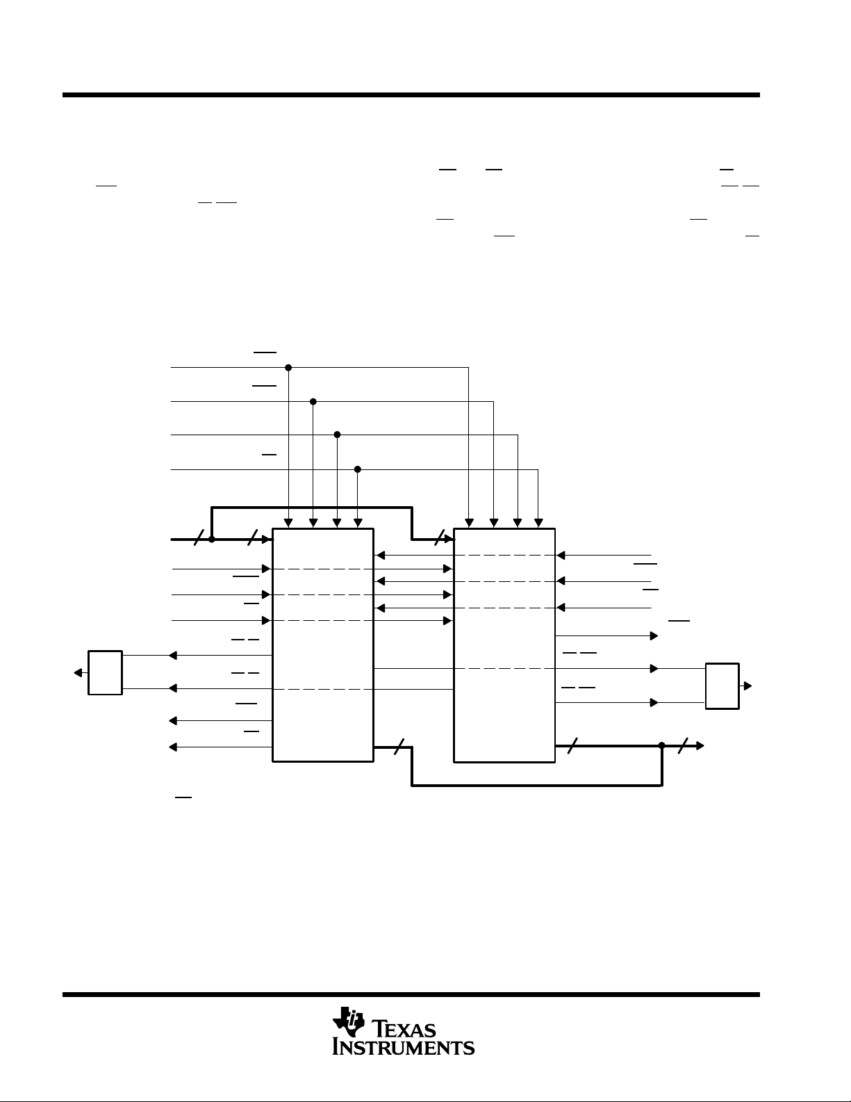
SN74V3640, SN74V3650, SN74V3660, SN74V3670, SN74V3680, SN74V3690
1024 × 36, 2048 × 36, 4096 × 36, 8192 × 36, 16384 × 36, 32768 × 36
3.3-V CMOS FIRST-IN, FIRST-OUT MEMORIES
SCAS668A – NOVEMBER 2001 – REVISED MARCH 2003
operating configurations
width-expansion configuration
Word width can be increased by connecting the control signals of multiple devices together. Status flags can
be detected from any one device. The exceptions are the EF
OR
functions in FWFT mode. Because of variations in skew between RCLK and WCLK, it is possible for EF/FF
deassertion and IR/OR assertion to vary by one cycle between FIFOs. In standard mode, such problems can
be avoided by creating composite flags, that is, ANDing EF
FIFO. In FWFT mode, composite flags can be created by ORing OR
of every FIFO.
Figure 23 demonstrates a width expansion using two SN74V3640, SN74V3650, SN74V3660, SN74V3670,
SN74V3680, and SN74V3690 devices. D0–D35 from each device form a 72-bit-wide input bus and Q0–Q35
from each device form a 72-bit-wide output bus. Any word width can be attained by adding additional
SN74V3640, SN74V3650, SN74V3660, SN74V3670, SN74V3680, and SN74V3690 devices.
Partial Reset (PRS)
and FF functions in standard mode and the IR and
of every FIFO and separately ANDing FF of every
of every FIFO and separately ORing IR
Master Reset (MRS
First-Word Fall-Through/Serial Input
Data In
PRODUCT PREVIEW
Gate
(see Note A)
m + n
Write Clock (WCLK)
Write Enable (WEN)
Full Flag/Input Ready 1
Full Flag/Input Ready 2
Programmable
Almost-Full Flag (PAF
Half-Full Flag (HF
(FWFT/SI)
Retransmit (RT
D0–Dm
m
Load (LD
(FF
(FF
)
/IR)
/IR)
)
)
)
)
(Dm + 1) – Dn
n
FIFO 1 FIFO 2
SN74V3640
SN74V3650
SN74V3660
SN74V3670
SN74V3680
SN74V3690
m
Q0–Qm
SN74V3640
SN74V3650
SN74V3660
SN74V3670
SN74V3680
SN74V3690
Read Clock (RCLK)
Read Enable (REN
Output Enable (OE
Programmable
Almost-Empty Flag (PAE
Empty Flag/Output Ready 1
(EF
/OR)
Empty Flag/Output Ready 2
/OR)
(EF
n
(Qm + 1) – Qn
)
)
)
(see Note A)
m + n
Gate
Data Out
NOTES: A. Use an OR
B. Do not connect any output control signals together directly.
C. FIFO 1 and FIFO 2 must be the same depth, but can be different word widths.
Figure 20. 1024 × 72, 2048 × 72, 4096 × 72, 8192 × 72, 16384 × 72, 32768 × 72
44
gate in FWFT mode and an AND gate in standard mode.
Width-Expansion Block Diagram
POST OFFICE BOX 655303 • DALLAS, TEXAS 75265

SN74V3640, SN74V3650, SN74V3660, SN74V3670, SN74V3680, SN74V3690
1024 × 36, 2048 × 36, 4096 × 36, 8192 × 36, 16384 × 36, 32768 × 36
3.3-V CMOS FIRST-IN, FIRST-OUT MEMORIES
SCAS668A – NOVEMBER 2001 – REVISED MARCH 2003
depth-expansion configuration (FWFT mode only)
The SN74V3640 easily can be adapted to applications requiring depths greater than 1024 for the SN74V3640,
2048 for the SN74V3650, 4096 for the SN74V3660, 8192 for the SN74V3670, 16384 for the SN74V3680, and
32768 for the SN74V3690, with an 18-bit bus width. In FWFT mode, the FIFOs can be connected in series (the
data outputs of one FIFO connected to the data inputs of the next), with no external logic necessary. The
resulting configuration provides a total depth equivalent to the sum of the depths associated with each single
FIFO. Figure 24 shows a depth expansion using two SN74V3640, SN74V3650, SN74V3660, SN74V3670,
SN74V3680, and SN74V3690 devices.
Care should be taken to select FWFT mode during master reset for all FIFOs in the depth-expansion
configuration. The first word written to an empty configuration passes from one FIFO to the next (ripple down)
until it finally appears at the outputs of the last FIFO in the chain. No read operation is necessary , but the RCLK
of each FIFO must be free running. Each time the data word appears at the outputs of one FIFO, that device’s
OR
line goes low, enabling a write to the next FIFO in line.
FWFT/SI
Transfer Clock
Write Clock
Write Enable
Input Ready Output Ready
Data In
n
FWFT/SI FWFT/SI
WCLK
WEN
IR
Dn
SN74V3640
SN74V3650
SN74V3660
SN74V3670
SN74V3680
SN74V3690
RCLK
OR
REN
OE
Qn
GND
nn
WCLK
WEN
IR
Dn
SN74V3640
SN74V3650
SN74V3660
SN74V3670
SN74V3680
SN74V3690
RCLK
REN
OR
OE
Qn
Read Clock
Read Enable
Output Enable
Data Out
Figure 21. 2048 × 36, 4096 × 36, 8192 × 36, 16384 × 36, 32768 × 36, 65536 × 36
Depth-Expansion Block Diagram
For an empty-expansion configuration, the amount of time it takes for OR
of the last FIFO in the chain to go low
(i.e., valid data to appear on the last FIFO’s outputs) after a word has been written to the first FIFO is the sum
of the delays for each FIFO:
(n–1) (4 transfer clock))3t
RCLK
(1)
Where:
n = number of FIFOs in the expansion
t
Note that extra cycles should be added for the possibility that the t
and the transfer clock, or RCLK and the transfer clock, for the OR
= RCLK period
RCLK
specification is not met between WCLK
sk1
flag.
The ripple-down delay is noticeable only for the first word written to an empty-depth-expansion configuration.
There will be no delay evident for subsequent words written to the configuration.
The first free location created by reading from a full-depth-expansion configuration will bubble up from the last
FIFO to the previous one until, finally , it moves into the first FIFO of the chain. Each time a free location is created
in one FIFO of the chain, that FIFO’s IR
line goes low, enabling the preceding FIFO to write a word to fill it.
PRODUCT PREVIEW
POST OFFICE BOX 655303 • DALLAS, TEXAS 75265
45

SN74V3640, SN74V3650, SN74V3660, SN74V3670, SN74V3680, SN74V3690
1024 × 36, 2048 × 36, 4096 × 36, 8192 × 36, 16384 × 36, 32768 × 36
3.3-V CMOS FIRST-IN, FIRST-OUT MEMORIES
SCAS668A – NOVEMBER 2001 – REVISED MARCH 2003
depth-expansion configuration (FWFT mode only) (continued)
For a full expansion configuration, the amount of time it takes for IR
a word has been read from the last FIFO is the sum of the delays for each individual FIFO:
of the first FIFO in the chain to go low after
(n–1) (3 transfer clock))2t
Where:
n = number of FIFOs in the expansion
= WCLK period
t
WCLK
Note that extra cycles should be added for the possibility that the t
and the transfer clock, or WCLK and the transfer clock, for the IR
The transfer-clock line should be tied to either WCLK or RCLK, whichever is faster. Both these actions result
in data moving as quickly as possible to the end of the chain and moving free locations to the beginning of the
chain.
WCLK
specification is not met between RCLK
sk1
flag.
(2)
PRODUCT PREVIEW
46
POST OFFICE BOX 655303 • DALLAS, TEXAS 75265

PACKAGE OPTION ADDENDUM
www.ti.com
30-Mar-2005
PACKAGING INFORMATION
Orderable Device Status
(1)
Package
Type
Package
Drawing
Pins Package
Qty
Eco Plan
SN74V3640-10PEU ACTIVE LQFP PEU 128 72 TBD Call TI Level-3-220C-168 HR
SN74V3640-15PEU ACTIVE LQFP PEU 128 72 TBD Call TI Level-3-220C-168 HR
SN74V3640-6PEU ACTIVE LQFP PEU 128 72 TBD Call TI Level-3-220C-168 HR
SN74V3640-7PEU ACTIVE LQFP PEU 128 72 TBD Call TI Level-3-220C-168 HR
SN74V3650-10PEU ACTIVE LQFP PEU 128 72 TBD Call TI Level-3-220C-168 HR
SN74V3650-15PEU ACTIVE LQFP PEU 128 72 TBD Call TI Level-3-220C-168 HR
SN74V3650-6PEU ACTIVE LQFP PEU 128 72 TBD Call TI Level-3-220C-168 HR
SN74V3650-7PEU ACTIVE LQFP PEU 128 72 TBD Call TI Level-3-220C-168 HR
SN74V3660-10PEU ACTIVE LQFP PEU 128 72 TBD Call TI Level-3-220C-168 HR
SN74V3660-15PEU ACTIVE LQFP PEU 128 72 TBD Call TI Level-3-220C-168 HR
SN74V3660-6PEU ACTIVE LQFP PEU 128 72 TBD Call TI Level-3-220C-168 HR
SN74V3660-7PEU ACTIVE LQFP PEU 128 72 TBD Call TI Level-3-220C-168 HR
SN74V3670-10PEU ACTIVE LQFP PEU 128 72 TBD Call TI Level-3-220C-168 HR
SN74V3670-15PEU ACTIVE LQFP PEU 128 72 TBD Call TI Level-3-220C-168 HR
SN74V3670-6PEU ACTIVE LQFP PEU 128 72 TBD Call TI Level-3-220C-168 HR
SN74V3670-7PEU ACTIVE LQFP PEU 128 72 TBD Call TI Level-3-220C-168 HR
SN74V3680-10PEU ACTIVE LQFP PEU 128 72 TBD Call TI Level-3-220C-168 HR
SN74V3680-15PEU ACTIVE LQFP PEU 128 72 TBD Call TI Level-3-220C-168 HR
SN74V3680-6PEU ACTIVE LQFP PEU 128 72 TBD Call TI Level-3-220C-168 HR
SN74V3680-7PEU ACTIVE LQFP PEU 128 72 TBD Call TI Level-3-220C-168 HR
SN74V3690-10PEU ACTIVE LQFP PEU 128 72 TBD Call TI Level-3-220C-168 HR
SN74V3690-15PEU ACTIVE LQFP PEU 128 72 TBD Call TI Level-3-220C-168 HR
SN74V3690-6PEU ACTIVE LQFP PEU 128 72 TBD Call TI Level-3-220C-168 HR
SN74V3690-7PEU ACTIVE LQFP PEU 128 72 TBD Call TI Level-3-220C-168 HR
(1)
The marketing status values are defined as follows:
ACTIVE: Product device recommended for new designs.
LIFEBUY: TI has announced that the device will be discontinued,and a lifetime-buy period is ineffect.
NRND: Not recommended for new designs. Device is in production to support existing customers, but TI does not recommend using this part in
a new design.
PREVIEW: Device has been announced but is not in production.Samples may or may not beavailable.
OBSOLETE: TI has discontinued the production of the device.
(2)
Lead/Ball Finish MSL Peak Temp
(3)
(2)
Eco Plan - The planned eco-friendly classification: Pb-Free (RoHS) or Green (RoHS & no Sb/Br) - please check
http://www.ti.com/productcontent for the latest availability information and additional product contentdetails.
TBD: The Pb-Free/Green conversion plan has not been defined.
Pb-Free (RoHS): TI's terms "Lead-Free" or "Pb-Free" mean semiconductor products that are compatible with the current RoHS requirements
for all 6 substances, including the requirement that lead not exceed 0.1% by weight in homogeneous materials. Where designed to be soldered
at high temperatures, TI Pb-Free products are suitable for usein specified lead-free processes.
Green (RoHS & no Sb/Br): TI defines "Green" to mean Pb-Free (RoHS compatible), and free of Bromine (Br) and Antimony (Sb) based flame
retardants (Br or Sb do not exceed 0.1% by weightin homogeneous material)
(3)
MSL, Peak Temp. -- The Moisture Sensitivity Level rating according to the JEDEC industry standard classifications, and peak solder
temperature.
Important Information and Disclaimer:The information provided on this page represents TI's knowledge and belief as of the date that it is
provided. TI bases its knowledge and belief on information provided by third parties, and makes no representation or warranty as to the
accuracy of such information. Efforts are underway to better integrate information from third parties. TI has taken and continues to take
Addendum-Page 1

PACKAGE OPTION ADDENDUM
www.ti.com
reasonable steps to provide representative and accurate information but may not have conducted destructive testing or chemical analysis on
incoming materials and chemicals. TI and TI suppliers consider certain information to be proprietary, and thus CAS numbers and other limited
information may not be available for release.
In no event shall TI's liability arising out of such information exceed the total purchase price of the TI part(s) at issue in this document sold by TI
to Customer on an annual basis.
30-Mar-2005
Addendum-Page 2

MECHANICAL DATA
MPQF058A – JANUARY 1998 – REVISED JUNE 1999
PEU (R-PQFP-G128) PLASTIC QUAD FLATPACK
103
128
102
1
0,50
18,50 TYP
20,20
19,80
22,20
21,80
0,27
0,17
0,08
65
38
M
64
12,50 TYP
39
14,20
13,80
16,20
15,80
0,13 NOM
Gage Plane
1,45
1,35
1,60 MAX
NOTES: A. All linear dimensions are in millimeters.
B. This drawing is subject to change without notice.
C. Falls within JEDEC MS-026
0,05 MIN
Seating Plane
0,08
0,25
0°–7°
0,75
0,45
4087743/B 10/98
POST OFFICE BOX 655303 • DALLAS, TEXAS 75265
1

IMPORTANT NOTICE
Texas Instruments Incorporated and its subsidiaries (TI) reserve the right to make corrections, modifications,
enhancements, improvements, and other changes to its products and services at any time and to discontinue
any product or service without notice. Customers should obtain the latest relevant information before placing
orders and should verify that such information is current and complete. All products are sold subject to TI’s terms
and conditions of sale supplied at the time of order acknowledgment.
TI warrants performance of its hardware products to the specifications applicable at the time of sale in
accordance with TI’s standard warranty. Testing and other quality control techniques are used to the extent TI
deems necessary to support this warranty . Except where mandated by government requirements, testing of all
parameters of each product is not necessarily performed.
TI assumes no liability for applications assistance or customer product design. Customers are responsible for
their products and applications using TI components. To minimize the risks associated with customer products
and applications, customers should provide adequate design and operating safeguards.
TI does not warrant or represent that any license, either express or implied, is granted under any TI patent right,
copyright, mask work right, or other TI intellectual property right relating to any combination, machine, or process
in which TI products or services are used. Information published by TI regarding third-party products or services
does not constitute a license from TI to use such products or services or a warranty or endorsement thereof.
Use of such information may require a license from a third party under the patents or other intellectual property
of the third party, or a license from TI under the patents or other intellectual property of TI.
Reproduction of information in TI data books or data sheets is permissible only if reproduction is without
alteration and is accompanied by all associated warranties, conditions, limitations, and notices. Reproduction
of this information with alteration is an unfair and deceptive business practice. TI is not responsible or liable for
such altered documentation.
Resale of TI products or services with statements different from or beyond the parameters stated by TI for that
product or service voids all express and any implied warranties for the associated TI product or service and
is an unfair and deceptive business practice. TI is not responsible or liable for any such statements.
Following are URLs where you can obtain information on other Texas Instruments products and application
solutions:
Products Applications
Amplifiers amplifier.ti.com Audio www.ti.com/audio
Data Converters dataconverter.ti.com Automotive www.ti.com/automotive
DSP dsp.ti.com Broadband www.ti.com/broadband
Interface interface.ti.com Digital Control www.ti.com/digitalcontrol
Logic logic.ti.com Military www.ti.com/military
Power Mgmt power.ti.com Optical Networking www.ti.com/opticalnetwork
Microcontrollers microcontroller.ti.com Security www.ti.com/security
Telephony www.ti.com/telephony
Video & Imaging www.ti.com/video
Wireless www.ti.com/wireless
Mailing Address: Texas Instruments
Post Office Box 655303 Dallas, Texas 75265
Copyright 2005, Texas Instruments Incorporated
 Loading...