Texas Instruments SN74TVC3010DBQR, SN74TVC3010DGVR, SN74TVC3010DW, SN74TVC3010DWR, SN74TVC3010PWR Datasheet

SN74TVC3010
10-BIT VOLTAGE CLAMP
SCDS088A – APRIL 1999 – REVISED JUNE 1999
D
Designed to be Used in Voltage-Limiting
Applications
D
6.5-Ω On-State Connection Between Ports
A and B
D
Flow-Through Pinout for Ease of Printed
Circuit Board Trace Routing
D
Direct Interface With GTL+ Levels
D
Package Options Include Plastic
Small-Outline (DW), Shrink Small-Outline
(DBQ), Thin Very Small-Outline (DGV), and
Thin Shrink Small-Outline (PW) Packages
description
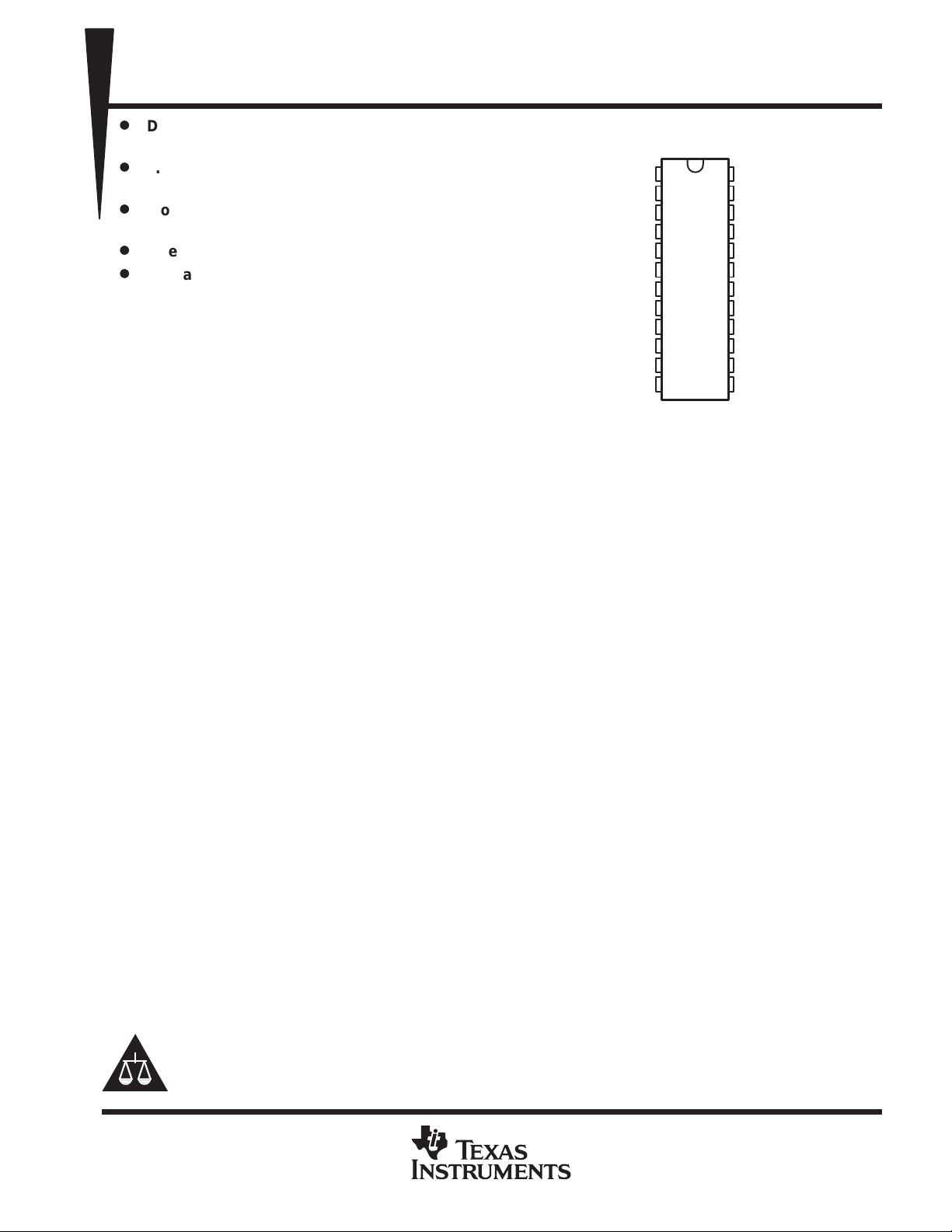
DBQ, DGV, DW, OR PW PACKAGE
GND
A1
A2
A3
A4
A5
A6
A7
A8
A9
A10
A1 1
(TOP VIEW)
1
24
2
23
3
22
4
21
5
20
6
19
7
18
8
17
9
16
10
15
11
14
12
13
GATE
B1
B2
B3
B4
B5
B6
B7
B8
B9
B10
B1 1
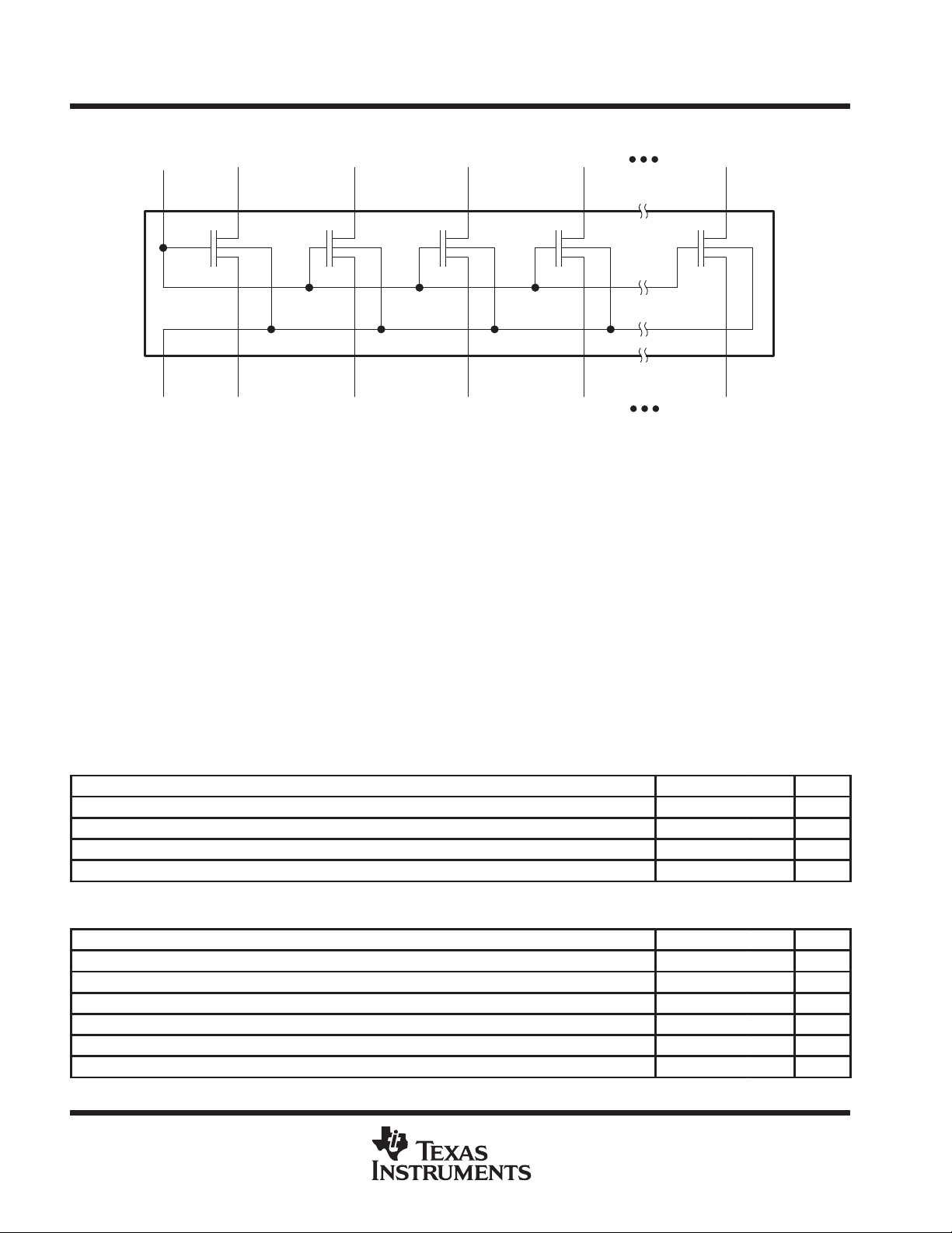
The SN74TVC3010 provides 11 parallel NMOS
pass transistors with a common gate. The low
on-state resistance of the switch allows
connections to be made with minimal propagation
delay .
The device can be used as a 10-bit switch with the gates cascaded together to a reference transistor. The
low-voltage side of each pass transistor is limited to a voltage set by the reference transistor. This is done to
protect components with inputs that are sensitive to high-state voltage-level overshoots. (See Application
Information in this data sheet.)
All of the transistors in the TVC array have the same electrical characteristics; therefore, any one of them can
be used as the reference transistor. Since, within the device, the characteristics from transistor-to-transistor are
equal, the maximum output high-state voltage (V
) will be approximately the reference voltage (V
OH
REF
), with
minimum deviation from one output to another. This is a large benefit of the TVC solution over discrete devices.
Because the fabrication of the transistors is symmetrical, either port connection of each bit can be used as the
low-voltage side, and the I/O signals are bidirectional through each FET.
The SN74TVC3010 is characterized for operation from –40°C to 85°C.
Please be aware that an important notice concerning availability, standard warranty, and use in critical applications of
Texas Instruments semiconductor products and disclaimers thereto appears at the end of this data sheet.
TI is a trademark of Texas Instruments Incorporated.
PRODUCTION DATA information is current as of publication date.
Products conform to specifications per the terms of Texas Instruments
standard warranty. Production processing does not necessarily include
testing of all parameters.
POST OFFICE BOX 655303 • DALLAS, TEXAS 75265
Copyright 1999, Texas Instruments Incorporated
1

SN74TVC3010
10-BIT VOLTAGE CLAMP
SCDS088A – APRIL 1999 – REVISED JUNE 1999
simplified schematic
GATE B1 B2 B3 B4 B11
24 23 22 21 20 13
12 3 4 5 12
GND A1 A2 A3 A4 A11
absolute maximum ratings over operating free-air temperature range (unless otherwise noted)
Input voltage range, V
Input/output voltage range, V
(see Note 1) –0.5 V to 7 V. . . . . . . . . . . . . . . . . . . . . . . . . . . . . . . . . . . . . . . . . . . . . . . . . .
I
(see Note 1) –0.5 V to 7 V. . . . . . . . . . . . . . . . . . . . . . . . . . . . . . . . . . . . . . . . . .
I/O
†
Continuous channel current 128 mA. . . . . . . . . . . . . . . . . . . . . . . . . . . . . . . . . . . . . . . . . . . . . . . . . . . . . . . . . . . . . .
Input clamp current, I
Package thermal impedance, θ
(V
< 0) –50 mA. . . . . . . . . . . . . . . . . . . . . . . . . . . . . . . . . . . . . . . . . . . . . . . . . . . . . . . . . . .
IK
I
(see Note 2): DBQ package 103°C/W. . . . . . . . . . . . . . . . . . . . . . . . . . . . . . .
JA
DGV package 139°C/W. . . . . . . . . . . . . . . . . . . . . . . . . . . . . . .
DW package 81°C/W. . . . . . . . . . . . . . . . . . . . . . . . . . . . . . . . .
PW package 120°C/W. . . . . . . . . . . . . . . . . . . . . . . . . . . . . . . .
Storage temperature range, T
†
Stresses beyond those listed under “absolute maximum ratings” may cause permanent damage to the device. These are stress ratings only, and
functional operation of the device at these or any other conditions beyond those indicated under “recommended operating conditions” is not
implied. Exposure to absolute-maximum-rated conditions for extended periods may affect device reliability.
NOTES: 1. The input and input/output negative-voltage ratings may be exceeded if the input and input/output clamp-current ratings are
observed.
2. The package thermal impedance is calculated in accordance with JESD 51.
–65°C to 150°C. . . . . . . . . . . . . . . . . . . . . . . . . . . . . . . . . . . . . . . . . . . . . . . . . . .
stg
recommended operating conditions
MIN TYP MAX UNIT
V
I/O
V
GATE
I
PASS
T
A
Input/output voltage 0 5 V
GATE voltage 0 5 V
Pass-transistor current 20 64 mA
Operating free-air temperature –40 85 °C
application operating conditions (see Figure 2)
2
V
BIAS
V
REF
V
DPU
I
PASS
I
REF
T
A
BIAS voltage 3 3.3 3.6 V
Reference voltage 1.365 1.5 1.635 V
Drain pullup voltage 2.36 2.5 2.64 V
Pass-transistor current 14 mA
Reference-transistor current 5 µA
Operating free-air temperature 0 85 °C
POST OFFICE BOX 655303 • DALLAS, TEXAS 75265
MIN TYP MAX UNIT

A or B
B or A
ns
SN74TVC3010
10-BIT VOLTAGE CLAMP
SCDS088A – APRIL 1999 – REVISED JUNE 1999
electrical characteristics over recommended operating free-air temperature range (unless
otherwise noted)
PARAMETER TEST CONDITIONS MIN TYP†MAX UNIT
V
IK
V
OL
C
i(GATE)
C
io(OFF)
C
io(ON)
‡
r
on
†
All typical values are at TA = 25°C.
‡
Measured by the voltage drop between the A and B terminals at the indicated current through the switch. On-state resistance is determined by
the lowest voltage of the two (A or B) terminals.
switching characteristics over recommended operating free-air temperature range,
= 2.36 V to 2.64 V (unless otherwise noted) (see Figure 1)
V
DPU
PARAMETER
t
PLH
t
PHL
V
= 0, II = –18 mA –1.2 V
BIAS
I
= 5 mA,
REF
V
= 2.625 V,
DPU
VI = 3 V or 0 24 pF
VO = 3 V or 0 4 12 pF
VO = 3 V or 0 12 30 pF
I
= 5 mA,
REF
V
= 2.625 V,
DPU
V
REF
R
DPU
V
REF
R
DPU
FROM
(INPUT)
= 1.365 V,
= 150 Ω,
= 1.365 V,
= 150 Ω,
VS = 0.175 V,
(see Figure 1)
VS = 0.175 V,
(see Figure 1)
TO
(OUTPUT)
350 mV
12.5 Ω
MIN MAX UNIT
0 4
0 4
POST OFFICE BOX 655303 • DALLAS, TEXAS 75265
3

SN74TVC3010
10-BIT VOLTAGE CLAMP
SCDS088A – APRIL 1999 – REVISED JUNE 1999
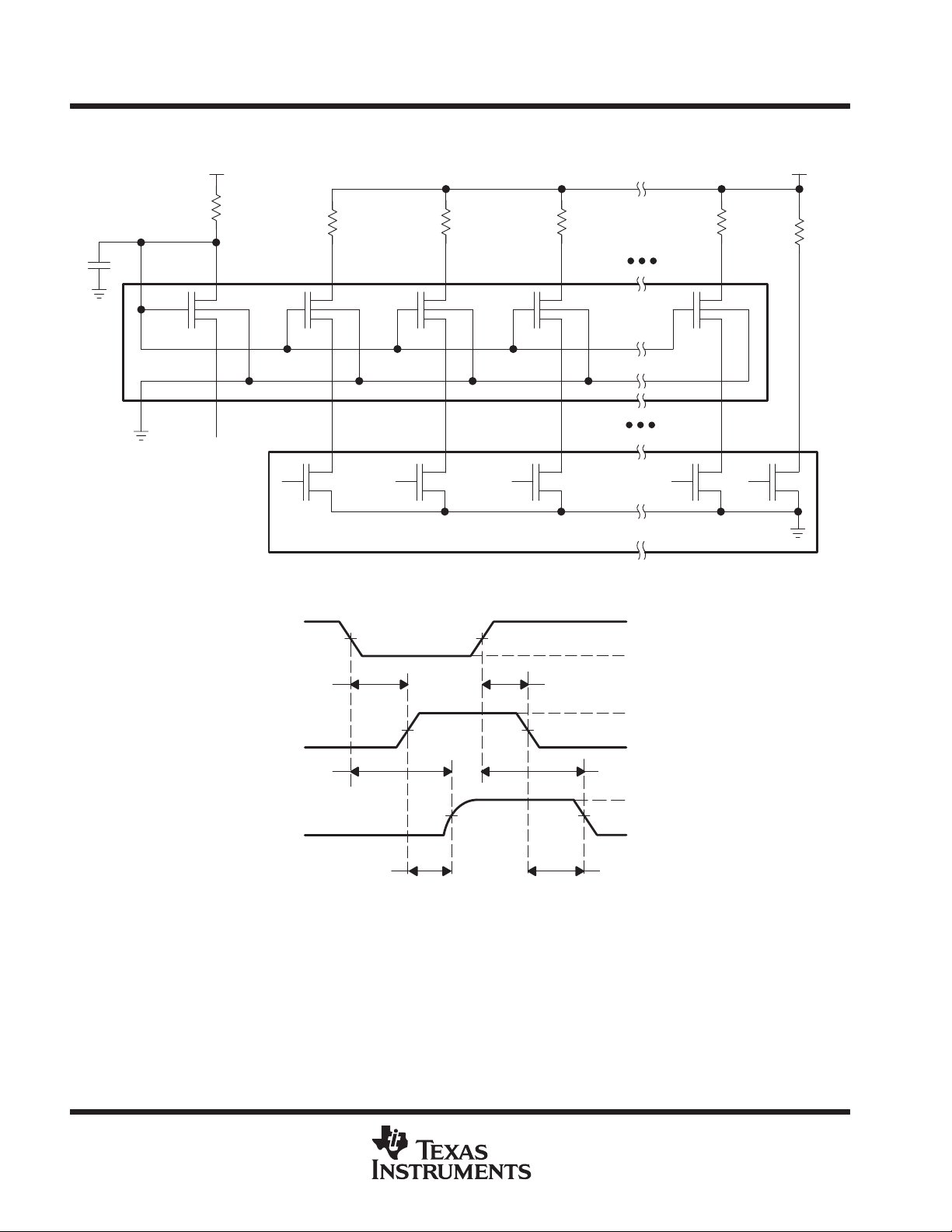
PARAMETER MEASUREMENT INFORMATION
Motherboard
Interface
GATE
24
TVC3010
1
3.3 V
200 kΩ
B1 (V
23
2
A1 (V
Open-Drain
Test Interface
BIAS
REF
V
DPU
R
R
R
=
DPU
150 Ω
)
)
B2
22
3
A2 (VS)
TESTER CALIBRATION SETUP (see Note D)
DPU
150 Ω
B3
21
4
A3 (VS)
=
DPU
150 Ω
B4
20
5
A4 (VS)
=
R
DPU
150 Ω
B11
13
12
A11 (VS)
=
Input
GATE
Tester
t
PLHREF
Output
Reference
t
PLHDUT
Output
Device
Under Test
(see Note E)
NOTES: A. CL includes probe and jig capacitance.
B. All input pulses are supplied by generators having the following characteristics: PRR ≤ 10 MHz, ZO = 50 Ω, tr ≤ 2 ns, tf ≤ 2 ns.
C. The outputs are measured one at a time with one transition per measurement.
D. Test procedure: t
E. t
F. t
t
PLHDUT
PLH
PHL
= t
PLHDUT
= t
PHLDUT
and t
PLHREF
PHLDUT
and t
PHLREF
are obtained by measuring the propagation delay of the device under test.
– t
PLHREF
– t
PHLREF
Figure 1. Tester Calibration Setup and Voltage Waveforms
2.5 V
1.25 V 1.25 V
0 V
t
PHLREF
2.5 V
1.25 V 1.25 V
V
OL
t
PHLDUT
2.5 V
1.25 V 1.25 V
V
OL
t
PLH
VOLTAGE WAVEFORMS
PROPAGATION DELAY TIMES
are obtained by measuring the propagation delay of a reference measuring point.
t
PHL
(see Note F)
4
POST OFFICE BOX 655303 • DALLAS, TEXAS 75265
 Loading...