

SN74SSTL16837A
20-BIT SSTL_3 INTERFACE UNIVERSAL BUS DRIVER
WITH 3-STATE OUTPUTS
SCBS675G – SEPTEMBER 1996 – REVISED SEPTEMBER 1998
1
POST OFFICE BOX 655303 • DALLAS, TEXAS 75265
D
Member of the Texas Instruments
Widebus
Family
D
Supports SSTL_3 Signal Inputs and
Outputs
D
Flow-Through Architecture Optimizes PCB
Layout
D
Meets SSTL_3 Class I and Class II
Specifications
D
Latch-Up Performance Exceeds 250 mA Per
JESD 17
D
Packaged in Plastic Thin Shrink
Small-Outline Package
description
This 20-bit universal bus driver is designed for 3-V
to 3.6-V V
CC
operation and SSTL_3 or L VTTL I/O
levels.
Data flow from A to Y is controlled by the
output-enable (OE
) input. The device operates in
the transparent mode when latch enable (LE) is
high. The A data is latched if LE is low and clock
(CLK) is held at a high or low logic level. If LE is
low, the A data is stored in the latch/flip-flop on the
low-to-high transition of CLK. When OE
is high,
the outputs are in the high-impedance state.
T o ensure the high-impedance state during power
up or power down, OE
should be tied to V
CC
through a pullup resistor; the minimum value of
the resistor is determined by the current-sinking
capability of the driver.
The SN74SSTL16837A is characterized for
operation from 0°C to 70°C.
Copyright 1998, Texas Instruments Incorporated
Widebus is a trademark of Texas Instruments Incorporated.
Please be aware that an important notice concerning availability, standard warranty, and use in critical applications of
Texas Instruments semiconductor products and disclaimers thereto appears at the end of this data sheet.
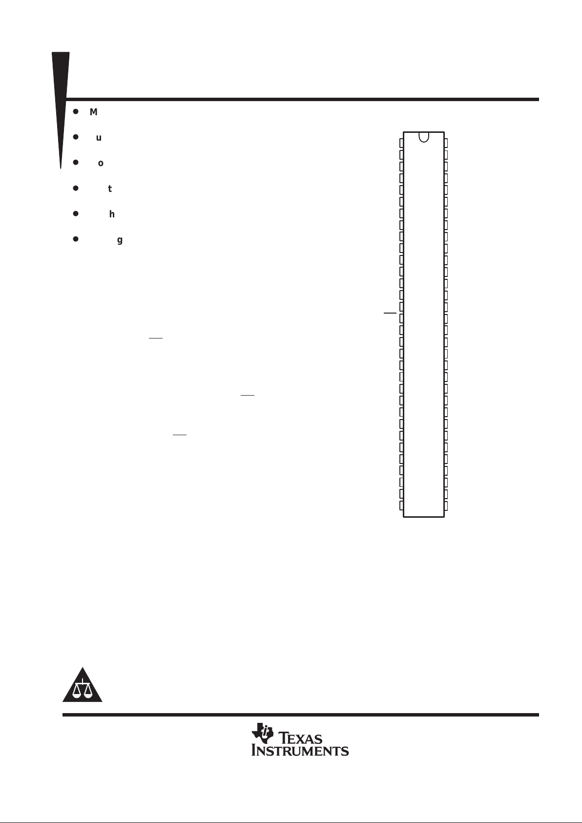
DGG PACKAGE
(TOP VIEW)
1
2
3
4
5
6
7
8
9
10
11
12
13
14
15
16
17
18
19
20
21
22
23
24
25
26
27
28
29
30
31
32
64
63
62
61
60
59
58
57
56
55
54
53
52
51
50
49
48
47
46
45
44
43
42
41
40
39
38
37
36
35
34
33
Y1
Y2
GND
Y3
Y4
V
DDQ
Y5
Y6
GND
Y7
Y8
V
DDQ
Y9
Y10
GND
OE
V
REF
GND
Y1 1
Y12
V
DDQ
Y13
Y14
GND
Y15
Y16
V
DDQ
Y17
Y18
GND
Y19
Y20
A1
A2
GND
A3
A4
V
CC
A5
A6
GND
A7
A8
V
CC
A9
A10
GND
CLK
LE
GND
A1 1
A12
V
CC
A13
A14
GND
A15
A16
V
CC
A17
A18
GND
A19
A20
PRODUCTION DATA information is current as of publication date.
Products conform to specifications per the terms of Texas Instruments
standard warranty. Production processing does not necessarily include
testing of all parameters.
SN74SSTL16837A
20-BIT SSTL_3 INTERFACE UNIVERSAL BUS DRIVER
WITH 3-STATE OUTPUTS
SCBS675G – SEPTEMBER 1996 – REVISED SEPTEMBER 1998
2
POST OFFICE BOX 655303 • DALLAS, TEXAS 75265
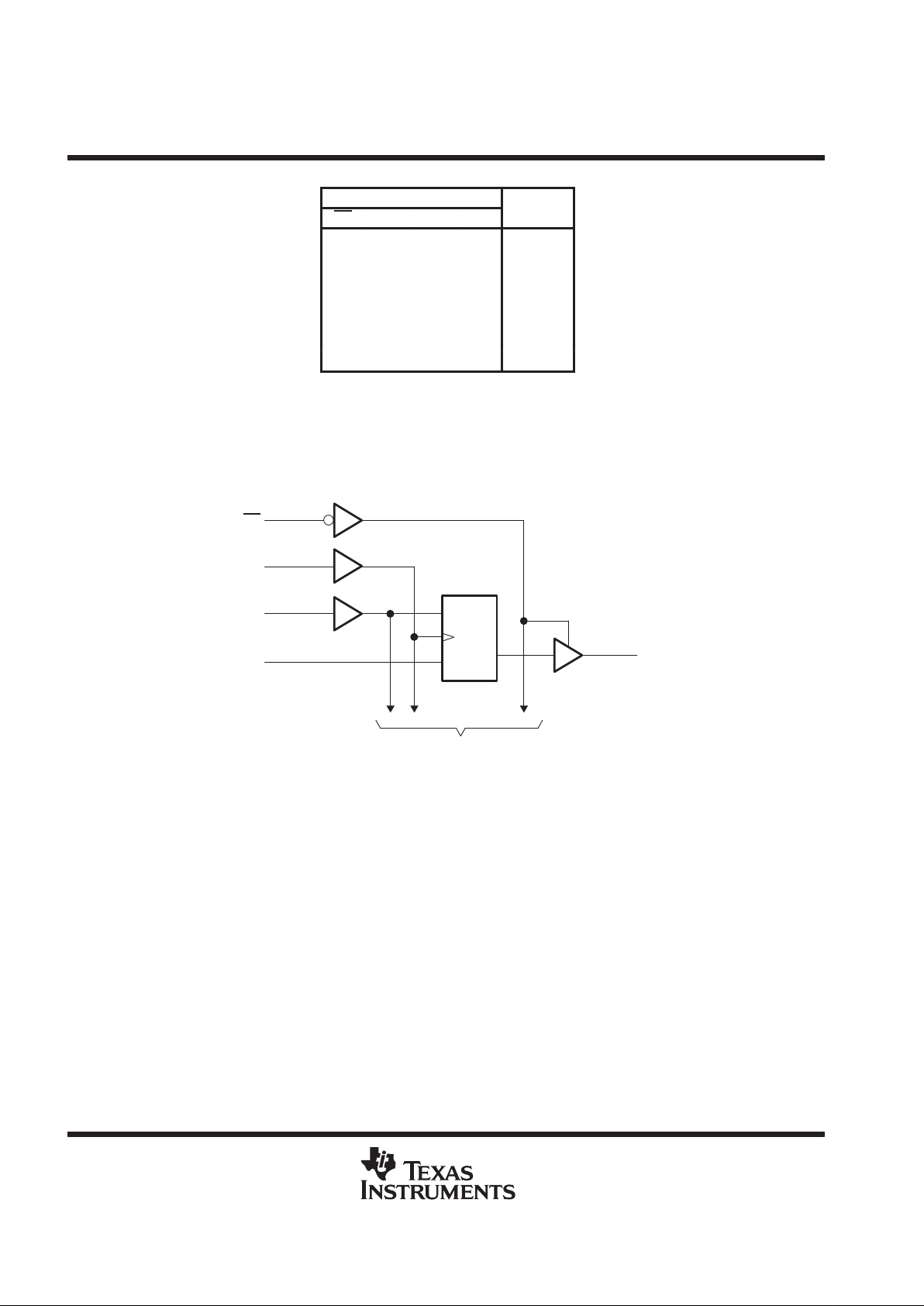
FUNCTION TABLE
INPUTS
OUTPUT
OE LE CLK A
Y
L H X H H
L HXL L
LL↑HH
LL↑LL
LLHX Y
0
†
LLLX Y
0
‡
HXXX Z
†
Output level before the indicated steady-state
input conditions were established, provided
that CLK was high before LE went low
‡
Output level before the indicated steady-state
input conditions were established
logic diagram (positive logic)
A1
CLK
LE
1D
To 19 Other Channels
C1
OE
Y1
LE
16
49
48
64
1
absolute maximum ratings over operating free-air temperature range (unless otherwise noted)
§
Supply voltage range, V
CC
or V
DDQ
–0.5 V to 4.6 V. . . . . . . . . . . . . . . . . . . . . . . . . . . . . . . . . . . . . . . . . . . . . . . . .
Input voltage range, V
I
(see Note 1) –0.5 V to VCC + 0.5 V. . . . . . . . . . . . . . . . . . . . . . . . . . . . . . . . . . . . . . . . . . .
Output voltage range, V
O
(see Notes 1 and 2) –0.5 V to V
DDQ
+ 0.5 V. . . . . . . . . . . . . . . . . . . . . . . . . . . . . . . .
Input clamp current, I
IK
(VI < 0) –50 mA. . . . . . . . . . . . . . . . . . . . . . . . . . . . . . . . . . . . . . . . . . . . . . . . . . . . . . . . . . .
Output clamp current, I
OK
(VO < 0) –50 mA. . . . . . . . . . . . . . . . . . . . . . . . . . . . . . . . . . . . . . . . . . . . . . . . . . . . . . . .
Continuous output current, I
O
(VO = 0 to V
DDQ
) ±50 mA. . . . . . . . . . . . . . . . . . . . . . . . . . . . . . . . . . . . . . . . . . . .
Continuous current through each V
CC
, V
DDQ
, or GND ±100 mA. . . . . . . . . . . . . . . . . . . . . . . . . . . . . . . . . . . . . .
Package thermal impedance, θ
JA
(see Note 3) 73°C/W. . . . . . . . . . . . . . . . . . . . . . . . . . . . . . . . . . . . . . . . . . . . .
Storage temperature range, T
stg
–65°C to 150°C. . . . . . . . . . . . . . . . . . . . . . . . . . . . . . . . . . . . . . . . . . . . . . . . . . .
§
Stresses beyond those listed under “absolute maximum ratings” may cause permanent damage to the device. These are stress ratings only, and
functional operation of the device at these or any other conditions beyond those indicated under “recommended operating conditions” is not
implied. Exposure to absolute-maximum-rated conditions for extended periods may affect device reliability.
NOTES: 1. The input and output negative-voltage ratings may be exceeded if the input and output clamp-current ratings are observed.
2. This current flows only when the output is in the high state and VO > V
DDQ
.
3. The package thermal impedance is calculated in accordance with JESD 51.
 Loading...