

Texas Instruments SN74S1051D, SN74S1051DR, SN74S1051N Datasheet
SN74S1051
12-BIT SCHOTTKY BARRIER DIODE
BUS-TERMINATION ARRAY
SDLS018A – SEPTEMBER 1990 – REVISED AUGUST 1997
D
Designed to Reduce Reflection Noise
D
Repetitive Peak Forward Current to 200 mA
D
12-Bit Array Structure Suited for
Bus-Oriented Systems
D
Package Options Include Plastic
Small-Outline Packages and Standard
Plastic 300-mil DIPs
description
This Schottky barrier diode bus-termination array
is designed to reduce reflection noise on memory
bus lines. This device consists of a 12-bit
high-speed Schottky diode array suitable for
clamping to V
and/or GND.
CC
The SN74S1051 is characterized for operation
from 0°C to 70°C.
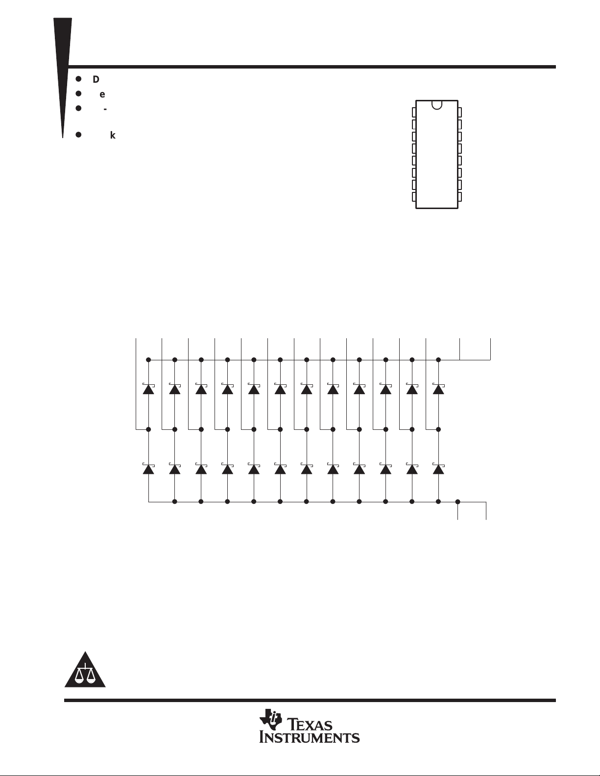
schematic diagrams
D012D023D034D045D056D067D078D089D0912D1013D1114D12
D OR N PACKAGE
(TOP VIEW)
V
1
CC
D01
2
D02
3
D03
4
D04
5
D05
6
D06
7
GND
8
15
16
15
14
13
12
11
10
V
CC
D12
D1 1
D10
D09
D08
D07
GND
9
V
CC
1
V
CC
16
Please be aware that an important notice concerning availability, standard warranty, and use in critical applications of
Texas Instruments semiconductor products and disclaimers thereto appears at the end of this data sheet.
PRODUCTION DATA information is current as of publication date.
Products conform to specifications per the terms of Texas Instruments
standard warranty. Production processing does not necessarily include
testing of all parameters.
POST OFFICE BOX 655303 • DALLAS, TEXAS 75265
8
GND9GND
Copyright 1997, Texas Instruments Incorporated
1
SN74S1051
To V
VFStatic forward voltage
V
From GND
IRStatic reverse current
V
V
A
CtTotal capacitance
pF
IxInternal crosstalk current
mA
12-BIT SCHOTTKY BARRIER DIODE
BUS-TERMINATION ARRAY
SDLS018A – SEPTEMBER 1990 – REVISED AUGUST 1997
absolute maximum ratings over operating free-air temperature range (unless otherwise noted)
Steady-state reverse voltage, V
Continuous forward current, I
Repetitive peak forward current
7 V. . . . . . . . . . . . . . . . . . . . . . . . . . . . . . . . . . . . . . . . . . . . . . . . . . . . . . . . . . . . .
R
: Any D terminal from GND or to VCC 50 mA. . . . . . . . . . . . . . . . . . . . . . . . . . .
F
Total through all GND or V
‡
, I
: Any D terminal from GND or VCC 200 mA. . . . . . . . . . . . . . . . . . . . .
FRM
Total through all GND or V
terminals 170 mA. . . . . . . . . . . . . . . . . . . . . . .
CC
terminals 1 A. . . . . . . . . . . . . . . . . . . .
CC
†
Continuous total power dissipation at (or below) 25°C free-air temperature (see Note 1) 625 mW. . . . . . . . . .
Operating free-air temperature range 0°C to 70°C. . . . . . . . . . . . . . . . . . . . . . . . . . . . . . . . . . . . . . . . . . . . . . . . . .
Storage temperature range, T
†
Stresses beyond those listed under “absolute maximum ratings” may cause permanent damage to the device. These are stress ratings only, and
functional operation of the device at these or any other conditions beyond those indicated under “recommended operating conditions” is not
implied. Exposure to absolute-maximum-rated conditions for extended periods may affect device reliability.
‡
These values apply for tw ≤ 100 µs, duty cycle ≤ 20%.
NOTE 1: For operation above 25°C free-air temperature, derate linearly at the rate of 5 m/W/°C.
–65°C to 150°C. . . . . . . . . . . . . . . . . . . . . . . . . . . . . . . . . . . . . . . . . . . . . . . . . . .
stg
electrical characteristics over recommended operating free-air temperature range (unless
otherwise noted)
single-diode operation (see Note 2)
PARAMETER TEST CONDITIONS MIN TYP§MAX UNIT
CC
V
Peak forward voltage IF = 200 mA 1.45 V
FM
To V
CC
From GND
p
§
All typical values are at VCC = 5 V, TA = 25°C.
NOTE 2: T est conditions and limits apply separately to each of the diodes. The diodes not under test are open-circuited during the measurement
of these characteristics.
VR = 0 V, f = 1 MHz 8 16
VR = 2 V, f = 1 MHz 4 8
IF = 18 mA 0.85 1.05
IF = 50 mA 1.05 1.3
IF = 18 mA 0.75 0.95
IF = 50 mA 0.95 1.2
= 7
R
5
µ
5
p
multiple-diode operation
§
All typical values are at VCC = 5 V, TA = 25°C.
NOTE 3: Ix is measured under the following conditions with one diode static, all others switching:
switching characteristics over recommended operating free-air temperature range (unless
otherwise noted) (see Figures 1 and 2)
PARAMETER TEST CONDITIONS MIN TYP MAX UNIT
t
Reverse recovery time IF = 10 mA, I
rr
2
PARAMETER TEST CONDITIONS MIN TYP§MAX UNIT
Total IF current = 1 A, See Note 3 0.8 2
Total IF current = 198 mA, See Note 3 0.02 0.2
Switching diodes: tw = 100 µs, duty cycle = 20%
Static diode: VR = 5 V
The static diode input current is the internal crosstalk current Ix.
RM(REC)
POST OFFICE BOX 655303 • DALLAS, TEXAS 75265
= 10 mA, I
= 1 mA, RL = 100 Ω 8 16 ns
R(REC)
SN74S1051
12-BIT SCHOTTKY BARRIER DIODE
BUS-TERMINATION ARRAY
SDLS018A – SEPTEMBER 1990 – REVISED AUGUST 1997
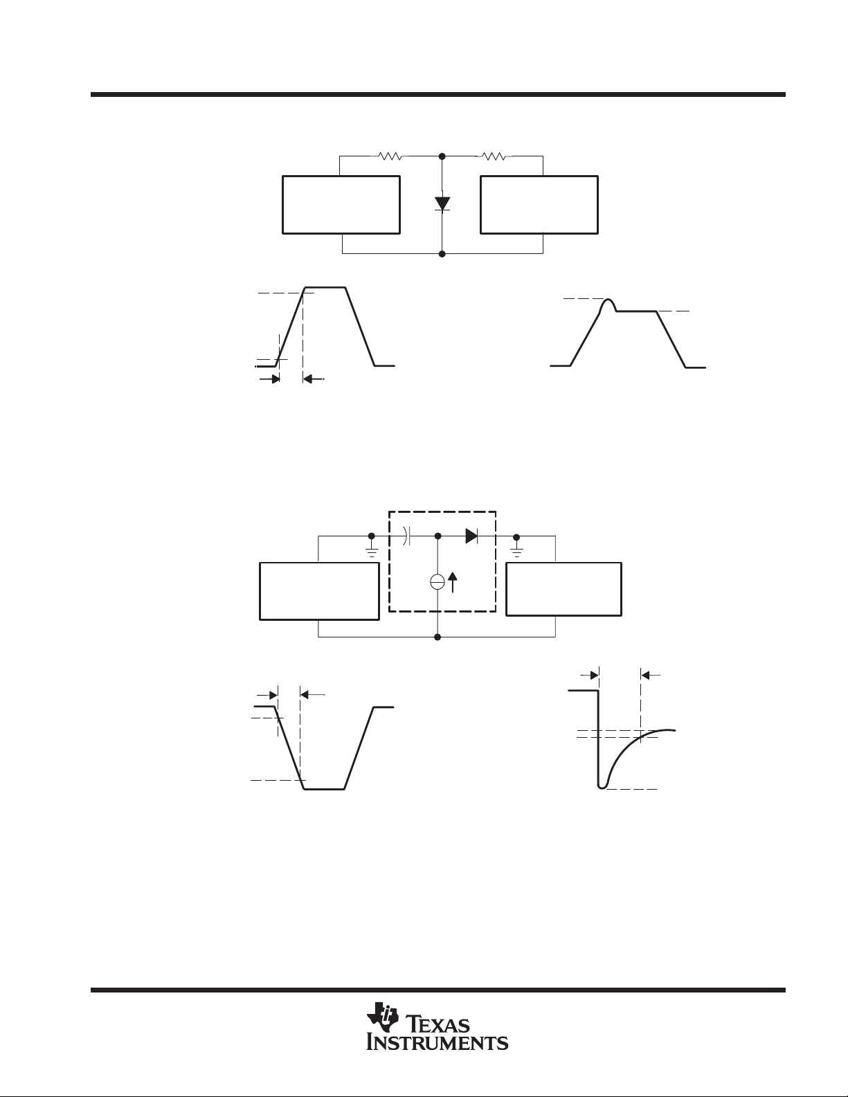
PARAMETER MEASUREMENT INFORMATION
50 Ω
(See Note A) (See Note B)
90%
Input Pulse
(See Note A)
10%
NOTES: A. The input pulse is supplied by a pulse generator having the following characteristics: tr = 20 ns, ZO = 50 Ω, freq = 500 Hz,
duty cycle = 1%.
B. The output waveform is monitored by an oscilloscope having the following characteristics: tr ≤ 350 ps, Ri = 50 Ω, Ci ≤ 5 pF.
Pulse
Generator
t
r
DUT
450 Ω
Oscilloscope
Output
Waveform
(See Note B)
Sampling
V
FM
V
F
Figure 1. Forward Recovery Voltage
DUT
(See Note A)
t
f
10%
Input Pulse
(See Note A)
90%
NOTES: A. The input pulse is supplied by a pulse generator having the following characteristics: tf = 0.5 ns, ZO = 50 Ω, tw ≥ 50 ns,
duty cycle = 1%.
B. The output waveform is monitored by an oscilloscope having the following characteristics: tr ≤ 350 ps, Ri = 50 Ω, Ci ≤ 5 pF.
Pulse
Generator
I
F
Output
Waveform
(See Note B)
Sampling
Oscilloscope
I
f
0
I
R(REC)
(See Note B)
t
rr
I
RM(REC)
Figure 2. Reverse Recovery Time
POST OFFICE BOX 655303 • DALLAS, TEXAS 75265
3
 Loading...