

TEXAS INSTRUMENTS SN54LVTH18512, SN54LVTH182512, SN74LVTH18512, SN74LVTH182512 Technical data
查询74LVTH182512DGGRE4供应商
SN54LVTH18512, SN54LVTH182512, SN74LVTH18512, SN74LVTH182512
3.3-V ABT SCAN TEST DEVICES
WITH 18-BIT UNIVERSAL BUS TRANSCEIVERS
SCBS671B – AUGUST 1996 – REVISED OCTOBER 1997
D
Members of the Texas Instruments
SCOPE
D
Members of the Texas Instruments
Widebus
D
State-of-the-Art 3.3-V ABT Design Supports
Family of Testability Products
Family
Mixed-Mode Signal Operation (5-V Input
and Output Voltages With 3.3-V VCC)
D
Support Unregulated Battery Operation
Down to 2.7 V
D
UBT
(Universal Bus Transceiver)
Combines D-Type Latches and D-Type
Flip-Flops for Operation in Transparent,
Latched, or Clocked Mode
D
Bus Hold on Data Inputs Eliminates the
Need for External Pullup/Pulldown
Resistors
D
B-Port Outputs of ’LVTH182512 Devices
Have Equivalent 25-Ω Series Resistors, So
No External Resistors Are Required
D
Compatible With the IEEE Std 1 149.1-1990
(JTAG) Test Access Port and
Boundary-Scan Architecture
D
SCOPE
Instruction Set
– IEEE Std 1149.1-1990 Required
Instructions and Optional CLAMP and
HIGHZ
– Parallel-Signature Analysis at Inputs
– Pseudo-Random Pattern Generation
From Outputs
– Sample Inputs/Toggle Outputs
– Binary Count From Outputs
– Device Identification
– Even-Parity Opcodes
D
Package Options Include 64-Pin Plastic
Thin Shrink Small Outline (DGG) and 64-Pin
Ceramic Dual Flat (HKC) Packages Using
0.5-mm Center-to-Center Spacings
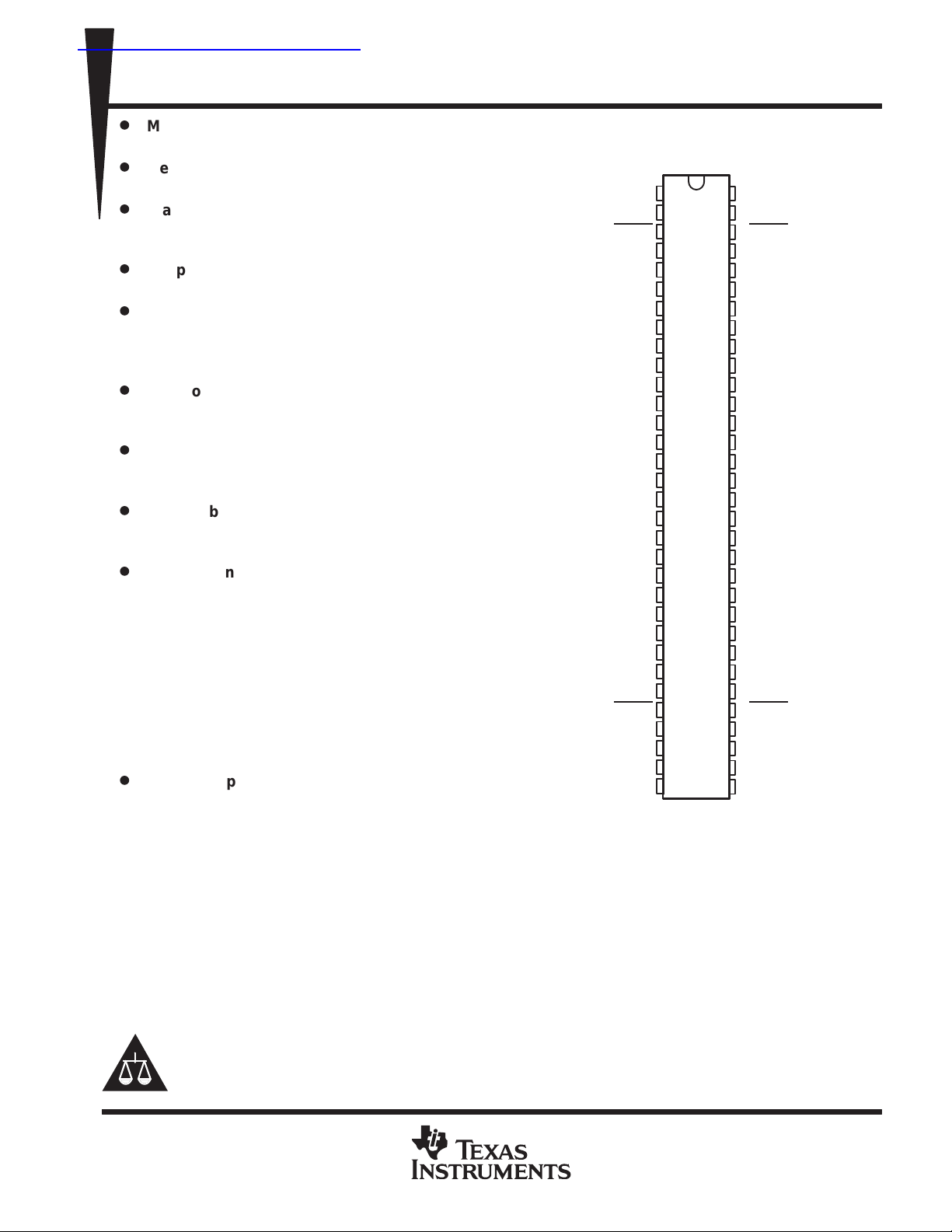
description
SN54LVTH18512, SN54LVTH182512 . . . HKC PACKAGE
SN74LVTH18512, SN74LVTH182512 . . . DGG PACKAGE
1CLKAB
1LEAB
1OEAB
2OEAB
2LEAB
2CLKAB
1A1
1A2
GND
1A3
1A4
1A5
V
CC
1A6
1A7
1A8
GND
1A9
2A1
2A2
2A3
GND
2A4
2A5
2A6
V
CC
2A7
2A8
2A9
GND
TDO
TMS
(TOP VIEW)
1
64
2
63
3
62
4
61
5
60
6
59
7
58
8
57
9
56
10
55
11
54
12
53
13
52
14
51
15
50
16
49
17
48
18
47
19
46
20
45
21
44
22
43
23
42
24
41
25
40
26
39
27
38
28
37
29
36
30
35
31
34
32
33
1CLKBA
1LEBA
1OEBA
1B1
1B2
GND
1B3
1B4
1B5
V
CC
1B6
1B7
1B8
GND
1B9
2B1
2B2
2B3
GND
2B4
2B5
2B6
V
CC
2B7
2B8
2B9
GND
2OEBA
2LEBA
2CLKBA
TDI
TCK
The ’LVTH18512 and ’LVTH182512 scan test devices with 18-bit universal bus transceivers are members of
the Texas Instruments SCOPE testability integrated-circuit family. This family of devices supports IEEE Std
1149.1-1990 boundary scan to facilitate testing of complex circuit-board assemblies. Scan access to the test
circuitry is accomplished via the 4-wire test access port (TAP) interface.
Additionally, these devices are designed specifically for low-voltage (3.3-V) VCC operation, but with the
capability to provide a TTL interface to a 5-V system environment.
Please be aware that an important notice concerning availability, standard warranty, and use in critical applications of
Texas Instruments semiconductor products and disclaimers thereto appears at the end of this data sheet.
SCOPE, Widebus, and UBT are trademarks of Texas Instruments Incorporated.
UNLESS OTHERWISE NOTED this document contains PRODUCTION
DATA information current as of publication date. Products conform to
specifications per the terms of Texas Instruments standard warranty.
Production processing does not necessarily include testing of all
parameters.
POST OFFICE BOX 655303 • DALLAS, TEXAS 75265
Copyright 1997, Texas Instruments Incorporated
1

SN54LVTH18512, SN54LVTH182512, SN74LVTH18512, SN74LVTH182512
3.3-V ABT SCAN TEST DEVICES
WITH 18-BIT UNIVERSAL BUS TRANSCEIVERS
SCBS671B – AUGUST 1996 – REVISED OCTOBER 1997
description (continued)
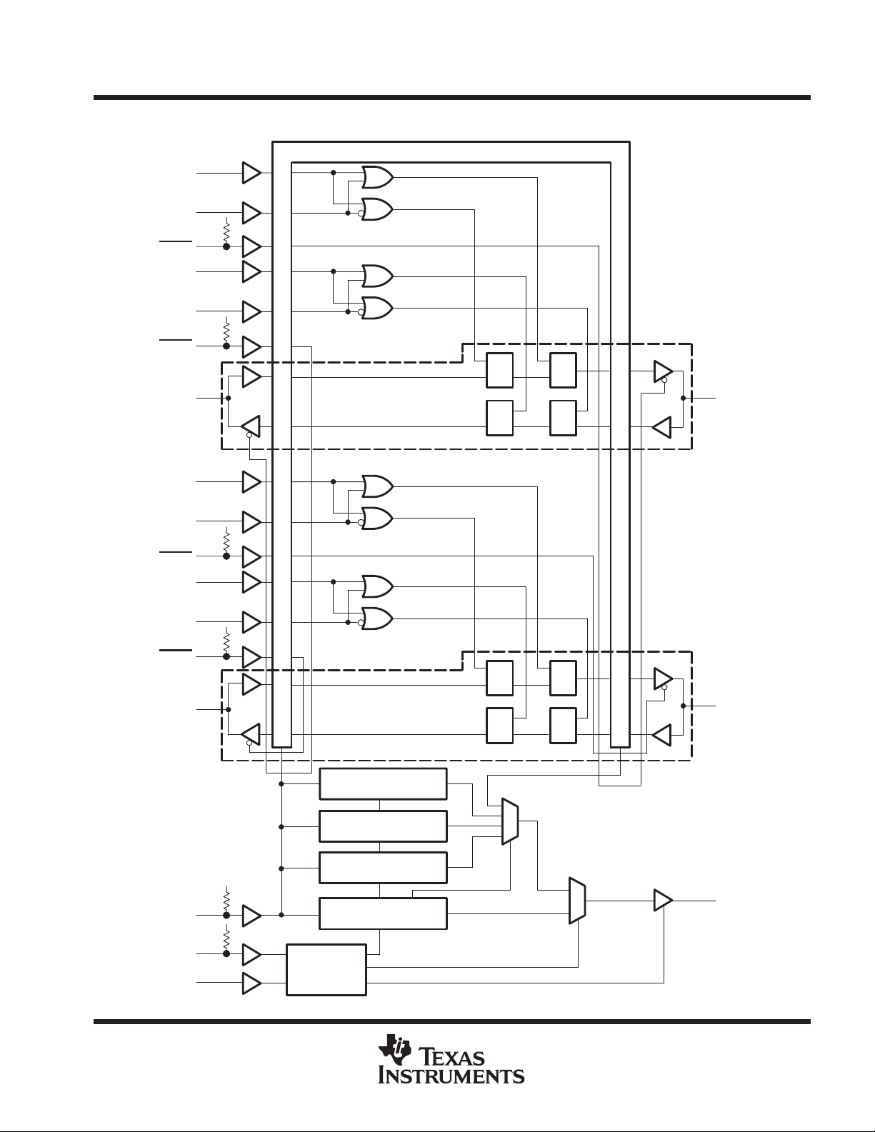
In the normal mode, these devices are 18-bit universal bus transceivers that combine D-type latches and D-type
flip-flops to allow data flow in transparent, latched, or clocked modes. They can be used either as two 9-bit
transceivers or one 18-bit transceiver. The test circuitry can be activated by the TAP to take snapshot samples
of the data appearing at the device pins or to perform a self test on the boundary-test cells. Activating the T AP
in the normal mode does not affect the functional operation of the SCOPE universal bus transceivers.
Data flow in each direction is controlled by output-enable (OEAB
and OEBA), latch-enable (LEAB and LEBA),
and clock (CLKAB and CLKBA) inputs. For A-to-B data flow, the devices operate in the transparent mode when
LEAB is high. When LEAB is low , the A data is latched while CLKAB is held at a static low or high logic level.
Otherwise, if LEAB is low, A data is stored on a low-to-high transition of CLKAB. When OEAB
is low, the B
outputs are active. When OEAB is high, the B outputs are in the high-impedance state. B-to-A data flow is similar
to A-to-B data flow but uses the OEBA, LEBA, and CLKBA inputs.
In the test mode, the normal operation of the SCOPE universal bus transceivers is inhibited, and the test
circuitry is enabled to observe and control the I/O boundary of the device. When enabled, the test circuitry
performs boundary-scan test operations according to the protocol described in IEEE Std 1149.1-1990.
Four dedicated test pins are used to observe and control the operation of the test circuitry: test data input (TDI),
test data output (TDO), test mode select (TMS), and test clock (TCK). Additionally, the test circuitry performs
other testing functions such as parallel-signature analysis (PSA) on data inputs and pseudo-random pattern
generation (PRPG) from data outputs. All testing and scan operations are synchronized to the T AP interface.
Active bus-hold circuitry is provided to hold unused or floating data inputs at a valid logic level.
The B-port outputs of ’L VTH182512, which are designed to source or sink up to 12 mA, include equivalent 25-Ω
series resistors to reduce overshoot and undershoot.
The SN54L VTH18512 and SN54LVTH182512 are characterized for operation over the full military temperature
range of –55°C to 125°C. The SN74LVTH18512 and SN74LVTH182512 are characterized for operation from
–40°C to 85°C.
FUNCTION TABLE
(normal mode, each register)
INPUTS
OEAB LEAB CLKAB A
L L L X B
L L ↑ LL
L L ↑ HH
L HXLL
L HXHH
H X X X Z
†
A-to-B data flow is shown. B-to-A data flow is similar
but uses OEBA
‡
Output level before the indicated steady-state input
conditions were established
, LEBA, and CLKBA.
†
OUTPUT
B
‡
0
2
POST OFFICE BOX 655303 • DALLAS, TEXAS 75265
SN54LVTH18512, SN54LVTH182512, SN74LVTH18512, SN74LVTH182512
functional block diagram
3.3-V ABT SCAN TEST DEVICES
WITH 18-BIT UNIVERSAL BUS TRANSCEIVERS
SCBS671B – AUGUST 1996 – REVISED OCTOBER 1997
1LEAB
1CLKAB
1OEAB
1LEBA
1CLKBA
1OEBA
1A1
2LEAB
2CLKAB
2OEAB
2LEBA
2
1
V
CC
3
63
64
V
CC
62
4
One of Nine Channels
29
30
V
CC
28
36
Boundary-Scan Register
C1
1D
C1
1D
C1
1D
C1
1D
61
1B1
2CLKBA
2OEBA
2A1
TDI
TMS
TCK
35
V
CC
37
C1
1D
16
C1
1D
One of Nine Channels
Bypass Register
Boundary-Control
Register
Identification
Register
V
CC
34
V
CC
32
33
Controller
Instruction
Register
TAP
C1
1D
C1
1D
49
31
2B1
TDO
POST OFFICE BOX 655303 • DALLAS, TEXAS 75265
3
SN54LVTH18512, SN54LVTH182512, SN74LVTH18512, SN74LVTH182512
3.3-V ABT SCAN TEST DEVICES
WITH 18-BIT UNIVERSAL BUS TRANSCEIVERS
SCBS671B – AUGUST 1996 – REVISED OCTOBER 1997
Terminal Functions
TERMINAL NAME DESCRIPTION
1A1–1A9,
2A1–2A9
1B1–1B9,
2B1–2B9
1CLKAB, 1CLKBA,
2CLKAB, 2CLKBA
GND Ground
1LEAB, 1LEBA,
2LEAB, 2LEBA
1OEAB, 1OEBA,
2OEAB
, 2OEBA
TCK
TDI
TDO
TMS
V
CC
Normal-function A-bus I/O ports. See function table for normal-mode logic.
Normal-function B-bus I/O ports. See function table for normal-mode logic.
Normal-function clock inputs. See function table for normal-mode logic.
Normal-function latch enables. See function table for normal-mode logic.
Normal-function output enables. See function table for normal-mode logic. An internal pullup at each terminal forces the
terminal to a high level if left unconnected.
Test clock. One of four terminals required by IEEE Std 1 149.1-1990. Test operations of the device are synchronous to
TCK. Data is captured on the rising edge of TCK and outputs change on the falling edge of TCK.
T est data input. One of four terminals required by IEEE Std 1 149.1-1990. TDI is the serial input for shifting data through
the instruction register or selected data register. An internal pullup forces TDI to a high level if left unconnected.
Test data output. One of four terminals required by IEEE Std 1149.1-1990. TDO is the serial output for shifting data
through the instruction register or selected data register.
Test mode select. One of four terminals required by IEEE Std 1149.1-1990. TMS directs the device through its TAP
controller states. An internal pullup forces TMS to a high level if left unconnected.
Supply voltage
4
POST OFFICE BOX 655303 • DALLAS, TEXAS 75265
SN54LVTH18512, SN54LVTH182512, SN74LVTH18512, SN74LVTH182512
3.3-V ABT SCAN TEST DEVICES
WITH 18-BIT UNIVERSAL BUS TRANSCEIVERS
SCBS671B – AUGUST 1996 – REVISED OCTOBER 1997
test architecture
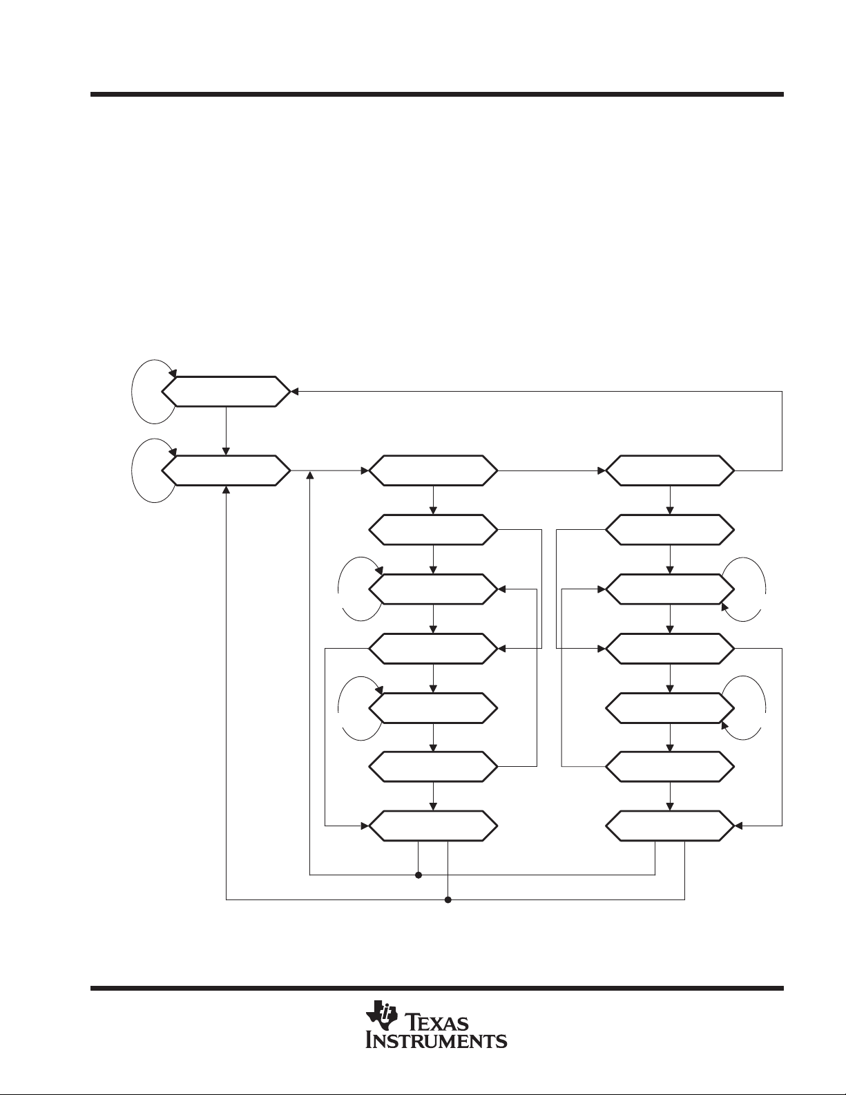
Serial-test information is conveyed by means of a 4-wire test bus or T AP , that conforms to IEEE Std 1149.1-1990.
T est instructions, test data, and test control signals all are passed along this serial-test bus. The TAP controller
monitors two signals from the test bus, TCK and TMS. The T AP controller extracts the synchronization (TCK)
and state control (TMS) signals from the test bus and generates the appropriate on-chip control signals for the
test structures in the device. Figure 1 shows the TAP-controller state diagram.
The T AP controller is fully synchronous to the TCK signal. Input data is captured on the rising edge of TCK and
output data changes on the falling edge of TCK. This scheme ensures data to be captured is valid for fully
one-half of the TCK cycle.
The functional block diagram shows the IEEE Std 1 149.1-1990 4-wire test bus and boundary-scan architecture
and the relationship among the test bus, the T AP controller, and the test registers. As shown, the device contains
an 8-bit instruction register and four test-data registers: a 48-bit boundary-scan register, a 3-bit
boundary-control register, a 1-bit bypass register, and a 32-bit device identification register.
Test-Logic-Reset
TMS = H
TMS = L
TMS = L
Run-Test/Idle Select-DR-Scan
TMS = L
Capture-DR
TMS = L
Shift-DR
TMS = L
TMS = H
TMS = H
Exit1-DR
TMS = L
Pause-DR
TMS = L
TMS = H
Exit2-DR
TMS = H
TMS = HTMS = H
TMS = H TMS = H
TMS = L
TMS = L
Select-IR-Scan
TMS = H
TMS = L
Capture-IR
TMS = L
Shift-IR
TMS = L
TMS = H
TMS = H
Exit1-IR
TMS = L
Pause-IR
TMS = L
TMS = H
Exit2-IR
TMS = H
Update-DR
TMS = LTMS = H
Figure 1. TAP-Controller State Diagram
POST OFFICE BOX 655303 • DALLAS, TEXAS 75265
Update-IR
TMS = LTMS = H
5

SN54LVTH18512, SN54LVTH182512, SN74LVTH18512, SN74LVTH182512
3.3-V ABT SCAN TEST DEVICES
WITH 18-BIT UNIVERSAL BUS TRANSCEIVERS
SCBS671B – AUGUST 1996 – REVISED OCTOBER 1997
state diagram description
The TAP controller is a synchronous finite-state machine that provides test control signals throughout the
device. The state diagram shown in Figure 1 is in accordance with IEEE Std 1 149.1-1990. The TAP controller
proceeds through its states based on the level of TMS at the rising edge of TCK.
As shown, the T AP controller consists of 16 states. There are six stable states (indicated by a looping arrow in
the state diagram) and ten unstable states. A stable state is a state the T AP controller can retain for consecutive
TCK cycles. Any state that does not meet this criterion is an unstable state.
There are two main paths through the state diagram: one to access and control the selected data register and
one to access and control the instruction register. Only one register can be accessed at a time.
Test-Logic-Reset
The device powers up in the T est-Logic-Reset state. In the stable Test-Logic-Reset state, the test logic is reset
and is disabled so that the normal logic function of the device is performed. The instruction register is reset to
an opcode that selects the optional IDCODE instruction, if supported, or the BYP ASS instruction. Certain data
registers can also be reset to their power-up values.
The state machine is constructed such that the T AP controller returns to the Test-Logic-Reset state in no more
than five TCK cycles if TMS is left high. The TMS pin has an internal pullup resistor that forces it high if left
unconnected or if a board defect causes it to be open circuited.
For the ’LVTH18512 and ’LVTH182512, the instruction register is reset to the binary value 10000001, which
selects the IDCODE instruction. Bits 47–44 in the boundary-scan register are reset to logic 1, ensuring that
these cells, which control A-port and B-port outputs, are set to benign values (i.e., if test mode were invoked
the outputs would be at the high-impedance state). Reset-value of other bits in the boundary-scan register
should be considered indeterminate. The boundary-control register is reset to the binary value 010, which
selects the PSA test operation.
Run-T est/Idle
The T AP controller must pass through the Run-T est/Idle state (from T est-Logic-Reset) before executing any test
operations. The Run-Test/Idle state also can be entered following data-register or instruction-register scans.
Run-Test/Idle is a stable state in which the test logic can be actively running a test or can be idle. The test
operations selected by the boundary-control register are performed while the TAP controller is in the
Run-Test/Idle state.
Select-DR-Scan, Select-lR-Scan
No specific function is performed in the Select-DR-Scan and Select-lR-Scan states, and the T AP controller exits
either of these states on the next TCK cycle. These states allow the selection of either data-register scan or
instruction-register scan.
Capture-DR
When a data-register scan is selected, the TAP controller must pass through the Capture-DR state. In the
Capture-DR state, the selected data register captures a data value as specified by the current instruction. Such
capture operations occur on the rising edge of TCK, upon which the T AP controller exits the Capture-DR state.
6
POST OFFICE BOX 655303 • DALLAS, TEXAS 75265

SN54LVTH18512, SN54LVTH182512, SN74LVTH18512, SN74LVTH182512
3.3-V ABT SCAN TEST DEVICES
WITH 18-BIT UNIVERSAL BUS TRANSCEIVERS
SCBS671B – AUGUST 1996 – REVISED OCTOBER 1997
Shift-DR
Upon entry to the Shift-DR state, the data register is placed in the scan path between TDI and TDO, and on the
first falling edge of TCK, TDO goes from the high-impedance state to an active state. TDO enables to the logic
level present in the least-significant bit of the selected data register.
While in the stable Shift-DR state, data is serially shifted through the selected data register on each TCK cycle.
The first shift occurs on the first rising edge of TCK after entry to the Shift-DR state (i.e., no shifting occurs during
the TCK cycle in which the T AP controller changes from Capture-DR to Shift-DR or from Exit2-DR to Shift-DR).
The last shift occurs on the rising edge of TCK, upon which the TAP controller exits the Shift-DR state.
Exit1-DR, Exit2-DR
The Exit1-DR and Exit2-DR states are temporary states that end a data-register scan. It is possible to return
to the Shift-DR state from either Exit1-DR or Exit2-DR without recapturing the data register. On the first falling
edge of TCK after entry to Exit1-DR, TDO goes from the active state to the high-impedance state.
Pause-DR
No specific function is performed in the stable Pause-DR state, in which the TAP controller can remain
indefinitely. The Pause-DR state suspends and resumes data-register scan operations without loss of data.
Update-DR
If the current instruction calls for the selected data register to be updated with current data, such update occurs
on the falling edge of TCK, following entry to the Update-DR state.
Capture-IR
When an instruction-register scan is selected, the TAP controller must pass through the Capture-IR state. In
the Capture-IR state, the instruction register captures its current status value. This capture operation occurs
on the rising edge of TCK, upon which the T AP controller exits the Capture-IR state. For the ’LVTH18512 and
’LVTH182512, the status value loaded in the Capture-IR state is the fixed binary value 10000001.
Shift-IR
Upon entry to the Shift-IR state, the instruction register is placed in the scan path between TDI and TDO. On
the first falling edge of TCK, TDO goes from the high-impedance state to the active state. TDO enables to the
logic level present in the least-significant bit of the instruction register.
While in the stable Shift-IR state, instruction data is serially shifted through the instruction register on each TCK
cycle. The first shift occurs on the first rising edge of TCK after entry to the Shift-IR state (i.e., no shifting occurs
during the TCK cycle in which the TAP controller changes from Capture-IR to Shift-IR or from Exit2-IR to
Shift-IR). The last shift occurs on the rising edge of TCK, upon which the T AP controller exits the Shift-IR state.
Exit1-IR, Exit2-IR
The Exit1-IR and Exit2-IR states are temporary states that end an instruction-register scan. It is possible to
return to the Shift-IR state from either Exit1-IR or Exit2-IR without recapturing the instruction register. On the
first falling edge of TCK after entry to Exit1-IR, TDO goes from the active state to the high-impedance state.
Pause-IR
No specific function is performed in the stable Pause-IR state, in which the TAP controller can remain
indefinitely. The Pause-IR state suspends and resumes instruction-register scan operations without loss
of data.
Update-IR
The current instruction is updated and takes effect on the falling edge of TCK, following entry to the
Update-IR state.
POST OFFICE BOX 655303 • DALLAS, TEXAS 75265
7
SN54LVTH18512, SN54LVTH182512, SN74LVTH18512, SN74LVTH182512
3.3-V ABT SCAN TEST DEVICES
WITH 18-BIT UNIVERSAL BUS TRANSCEIVERS
SCBS671B – AUGUST 1996 – REVISED OCTOBER 1997
register overview
With the exception of the bypass and device-identification registers, any test register can be thought of as a
serial shift register with a shadow latch on each bit. The bypass and device-identification registers differ in that
they contain only a shift register. During the appropriate capture state (Capture-IR for instruction register,
Capture-DR for data registers), the shift register can be parallel loaded from a source specified by the current
instruction. During the appropriate shift state (Shift-IR or Shift-DR), the contents of the shift register are shifted
out from TDO while new contents are shifted in at TDI. During the appropriate update state (Update-IR or
Update-DR), the shadow latches are updated from the shift register.
instruction register description
The instruction register (IR) is eight bits long and tells the device what instruction is to be executed. Information
contained in the instruction includes the mode of operation (either normal mode, in which the device performs
its normal logic function, or test mode, in which the normal logic function is inhibited or altered), the test operation
to be performed, which of the four data registers is to be selected for inclusion in the scan path during
data-register scans, and the source of data to be captured into the selected data register during Capture-DR.
T able 3 lists the instructions supported by the ’L VTH18512 and ’L VTH182512. The even-parity feature specified
for SCOPE devices is supported in this device. Bit 7 of the instruction opcode is the parity bit. Any instructions
that are defined for SCOPE devices but are not supported by this device default to BYPASS.
During Capture-IR, the IR captures the binary value 10000001. As an instruction is shifted in, this value is shifted
out via TDO and can be inspected as verification that the IR is in the scan path. During Update-IR, the value
that has been shifted into the IR is loaded into shadow latches. At this time, the current instruction is updated
and any specified mode change takes effect. At power up or in the Test-Logic-Reset state, the IR is reset to the
binary value 10000001, which selects the IDCODE instruction. The IR order of scan is shown in Figure 2.
Bit 7
Parity
(MSB)
Bit 6 Bit 5 Bit 4 Bit 3 Bit 2 Bit 1
Bit 0
(LSB)
TDOTDI
Figure 2. Instruction Register Order of Scan
8
POST OFFICE BOX 655303 • DALLAS, TEXAS 75265
SN54LVTH18512, SN54LVTH182512, SN74LVTH18512, SN74LVTH182512
3.3-V ABT SCAN TEST DEVICES
WITH 18-BIT UNIVERSAL BUS TRANSCEIVERS
SCBS671B – AUGUST 1996 – REVISED OCTOBER 1997
data register description
boundary-scan register
The boundary-scan register (BSR) is 48 bits long. It contains one boundary-scan cell (BSC) for each
normal-function input pin and one BSC for each normal-function I/O pin (one single cell for both input data and
output data). The BSR is used to store test data that is to be applied externally to the device output pins, and/or
to capture data that appears internally at the outputs of the normal on-chip logic and/or externally at the device
input pins.
The source of data to be captured into the BSR during Capture-DR is determined by the current instruction. The
contents of the BSR can change during Run-Test/Idle as determined by the current instruction. At power up or
in T est-Logic-Reset, BSCs 47–44 are reset to logic 1, ensuring that these cells, which control A-port and B-port
outputs are set to benign values (i.e., if test mode were invoked, the outputs would be at the high-impedance
state). Reset values of other BSCs should be considered indeterminate.
The BSR order of scan is from TDI through bits 47–0 to TDO. T able 1 shows the BSR bits and their associated
device pin signals.
Table 1. Boundary-Scan Register Configuration
BSR BIT
NUMBER
47 2OEAB 35 2A9-I/O 17 2B9-I/O
46 1OEAB 34 2A8-I/O 16 2B8-I/O
45 2OEBA 33 2A7-I/O 15 2B7-I/O
44 1OEBA 32 2A6-I/O 14 2B6-I/O
43 2CLKAB 31 2A5-I/O 13 2B5-I/O
42 1CLKAB 30 2A4-I/O 12 2B4-I/O
41 2CLKBA 29 2A3-I/O 11 2B3-I/O
40 1CLKBA 28 2A2-I/O 10 2B2-I/O
39 2LEAB 27 2A1-I/O 9 2B1-I/O
38 1LEAB 26 1A9-I/O 8 1B9-I/O
37 2LEBA 25 1A8-I/O 7 1B8-I/O
36 1LEBA 24 1A7-I/O 6 1B7-I/O
–– –– 23 1A6-I/O 5 1B6-I/O
–– –– 22 1A5-I/O 4 1B5-I/O
–– –– 21 1A4-I/O 3 1B4-I/O
–– –– 20 1A3-I/O 2 1B3-I/O
–– –– 19 1A2-I/O 1 1B2-I/O
–– –– 18 1A1-I/O 0 1B1-I/O
DEVICE
SIGNAL
BSR BIT
NUMBER
DEVICE
SIGNAL
BSR BIT
NUMBER
DEVICE
SIGNAL
POST OFFICE BOX 655303 • DALLAS, TEXAS 75265
9
SN54LVTH18512, SN54LVTH182512, SN74LVTH18512, SN74LVTH182512
3.3-V ABT SCAN TEST DEVICES
WITH 18-BIT UNIVERSAL BUS TRANSCEIVERS
SCBS671B – AUGUST 1996 – REVISED OCTOBER 1997
boundary-control register
The boundary-control register (BCR) is three bits long. The BCR is used in the context of the boundary-run test
(RUNT) instruction to implement additional test operations not included in the basic SCOPE instruction set.
Such operations include PRPG, PSA, and binary count up (COUNT). Table 4 shows the test operations that
are decoded by the BCR.
During Capture-DR, the contents of the BCR are not changed. At power up or in Test-Logic-Reset, the BCR is
reset to the binary value 010, which selects the PSA test operation. The BCR order of scan is shown in Figure 3.
Bit 2
(MSB)
Bit 1
Bit 0
(LSB)
TDOTDI
Figure 3. Boundary-Control Register Order of Scan
bypass register
The bypass register is a 1-bit scan path that can be selected to shorten the length of the system scan path,
reducing the number of bits per test pattern that must be applied to complete a test operation. During
Capture-DR, the bypass register captures a logic 0. The bypass register order of scan is shown in Figure 4.
Bit 0
TDOTDI
Figure 4. Bypass Register Order of Scan
10
POST OFFICE BOX 655303 • DALLAS, TEXAS 75265
SN54LVTH18512, SN54LVTH182512, SN74LVTH18512, SN74LVTH182512
3.3-V ABT SCAN TEST DEVICES
WITH 18-BIT UNIVERSAL BUS TRANSCEIVERS
SCBS671B – AUGUST 1996 – REVISED OCTOBER 1997
device-identification register
The device-identification register (IDR) is 32 bits long. It can be selected and read to identify the manufacturer,
part number, and version of this device.
For the ’LVTH18512, the binary value 00000000000000111011000000101111 (0003B02F, hex) is captured
(during Capture-DR state) in the IDR to identify this device as Texas Instruments SN54/74LVTH18512.
For the ’LVTH182512, the binary value 00000000000000111100000000101111 (0003C02F, hex) is captured
(during Capture-DR state) in the device-identification register to identify this device as Texas Instruments
SN54/74LVTH182512.
The IDR order of scan is from TDI through bits 31–0 to TDO. T able 2 shows the IDR bits and their significance.
Table 2. Device-Identification Register Configuration
IDR BIT
NUMBER
31 VERSION3 27 PAR TNUMBER15 11 MANUFACTURER10
30 VERSION2 26 PARTNUMBER14 10 MANUFACTURER09
29 VERSION1 25 PARTNUMBER13 9 MANUFACTURER08
28 VERSION0 24 PARTNUMBER12 8 MANUFACTURER07
–– –– 23 PARTNUMBER11 7 MANUFACTURER06
–– –– 22 PARTNUMBER10 6 MANUFACTURER05
–– –– 21 PARTNUMBER09 5 MANUFACTURER04
–– –– 20 PARTNUMBER08 4 MANUFACTURER03
–– –– 19 PARTNUMBER07 3 MANUFACTURER02
–– –– 18 PARTNUMBER06 2 MANUFACTURER01
–– –– 17 PARTNUMBER05 1 MANUFACTURER00
–– –– 16 PARTNUMBER04 0 LOGIC1
–– –– 15 PARTNUMBER03 –– ––
–– –– 14 PARTNUMBER02 –– ––
–– –– 13 PARTNUMBER01 –– ––
–– –– 12 PARTNUMBER00 –– ––
†
Note that for TI products, bits 11–0 of the device-identification register always contain the binary value 000000101111
(02F, hex).
IDENTIFICATION
SIGNIFICANCE
IDR BIT
NUMBER
IDENTIFICATION
SIGNIFICANCE
IDR BIT
NUMBER
IDENTIFICATION
SIGNIFICANCE
†
†
†
†
†
†
†
†
†
†
†
†
POST OFFICE BOX 655303 • DALLAS, TEXAS 75265
11

SN54LVTH18512, SN54LVTH182512, SN74LVTH18512, SN74LVTH182512
3.3-V ABT SCAN TEST DEVICES
WITH 18-BIT UNIVERSAL BUS TRANSCEIVERS
SCBS671B – AUGUST 1996 – REVISED OCTOBER 1997
instruction-register opcode description
The instruction-register opcodes are shown in Table 3. The following descriptions detail the operation of
each instruction.
Table 3. Instruction-Register Opcodes
BINARY CODE
BIT 7 → BIT 0
MSB → LSB
00000000 EXTEST Boundary scan Boundary scan Test
10000001 IDCODE Identification read Device identification Normal
10000010 SAMPLE/PRELOAD Sample boundary Boundary scan Normal
0000001 1 BYPASS
10000100 BYPASS
00000101 BYPASS
00000110 HIGHZ Control boundary to high impedance Bypass Modified test
100001 11 CLAMP Control boundary to 1/0 Bypass Test
10001000 BYPASS
00001001 RUNT Boundary-run test Bypass Test
00001010 READBN Boundary read Boundary scan Normal
1000101 1 READBT Boundary read Boundary scan Test
00001 100 CELLTST Boundary self test Boundary scan Normal
10001 101 TOPHIP Boundary toggle outputs Bypass Test
10001 110 SCANCN Boundary-control register scan Boundary control Normal
00001 11 1 SCANCT Boundary-control register scan Boundary control Test
All others BYP ASS Bypass scan Bypass Normal
†
Bit 7 is used to maintain even parity in the 8-bit instruction.
‡
The BYPASS instruction is executed in lieu of a SCOPE instruction that is not supported in the ’LVTH18512 or ’LVTH182512.
†
SCOPE OPCODE DESCRIPTION
‡
‡
‡
‡
SELECTED DATA
REGISTER
Bypass scan Bypass Normal
Bypass scan Bypass Normal
Bypass scan Bypass Normal
Bypass scan Bypass Normal
MODE
boundary scan
This instruction conforms to the IEEE Std 1149.1-1990 EXTEST instruction. The BSR is selected in the scan
path. Data appearing at the device input and I/O pins is captured in the associated BSCs. Data that has been
scanned into the I/O BSCs for pins in the output mode is applied to the device I/O pins. Data present at the device
pins, except for output enables, is passed through the BSCs to the normal on-chip logic. For I/O pins, the
operation of a pin as input or output is determined by the contents of the output-enable BSCs (bits 47–44 of the
BSR). When a given output enable is active (logic 0), the associated I/O pins operate in the output mode.
Otherwise, the I/O pins operate in the input mode. The device operates in the test mode.
identification read
This instruction conforms to the IEEE Std 1149.1-1990 IDCODE instruction. The IDR is selected in the scan
path. The device operates in the normal mode.
sample boundary
This instruction conforms to the IEEE Std 1 149.1-1990 SAMPLE/PRELOAD instruction. The BSR is selected
in the scan path. Data appearing at the device input pins and I/O pins in the input mode is captured in the
associated BSCs, while data appearing at the outputs of the normal on-chip logic is captured in the BSCs
associated with I/O pins in the output mode. The device operates in the normal mode.
12
POST OFFICE BOX 655303 • DALLAS, TEXAS 75265

SN54LVTH18512, SN54LVTH182512, SN74LVTH18512, SN74LVTH182512
3.3-V ABT SCAN TEST DEVICES
WITH 18-BIT UNIVERSAL BUS TRANSCEIVERS
SCBS671B – AUGUST 1996 – REVISED OCTOBER 1997
bypass scan
This instruction conforms to the IEEE Std 1 149.1-1990 BYP ASS instruction. The bypass register is selected in
the scan path. A logic 0 value is captured in the bypass register during Capture-DR. The device operates in the
normal mode.
control boundary to high impedance
This instruction conforms to the IEEE Std 1 149.1a-1993 HIGHZ instruction. The bypass register is selected in
the scan path. A logic 0 value is captured in the bypass register during Capture-DR. The device operates in a
modified test mode in which all device I/O pins are placed in the high-impedance state, the device input pins
remain operational, and the normal on-chip logic function is performed.
control boundary to 1/0
This instruction conforms to the IEEE Std 1 149.1a-1993 CLAMP instruction. The bypass register is selected in
the scan path. A logic 0 value is captured in the bypass register during Capture-DR. Data in the I/O BSCs for
pins in the output mode is applied to the device I/O pins. The device operates in the test mode.
boundary-run test
The bypass register is selected in the scan path. A logic 0 value is captured in the bypass register during
Capture-DR. The device operates in the test mode. The test operation specified in the BCR is executed during
Run-Test /Idle. The five test operations decoded by the BCR are: sample inputs/toggle outputs (TOPSIP),
PRPG, PSA, simultaneous PSA and PRPG (PSA/PRPG), and simultaneous PSA and binary count up
(PSA/COUNT).
boundary read
The BSR is selected in the scan path. The value in the BSR remains unchanged during Capture-DR. This
instruction is useful for inspecting data after a PSA operation.
boundary self test
The BSR is selected in the scan path. All BSCs capture the inverse of their current values during Capture-DR.
In this way , the contents of the shadow latches can be read out to verify the integrity of both shift-register and
shadow-latch elements of the BSR. The device operates in the normal mode.
boundary toggle outputs
The bypass register is selected in the scan path. A logic 0 value is captured in the bypass register during
Capture-DR. Data in the shift-register elements of the selected output-mode BSCs is toggled on each rising
edge of TCK in Run-T est/Idle and is then updated in the shadow latches and thereby applied to the associated
device I/O pins on each falling edge of TCK in Run-Test/Idle. Data in the input-mode BSCs remains constant.
Data appearing at the device input or I/O pins is not captured in the input-mode BSCs. The device operates in
the test mode.
boundary-control-register scan
The BCR is selected in the scan path. The value in the BCR remains unchanged during Capture-DR. This
operation must be performed before a boundary-run test operation to specify which test operation is to
be executed.
POST OFFICE BOX 655303 • DALLAS, TEXAS 75265
13

SN54LVTH18512, SN54LVTH182512, SN74LVTH18512, SN74LVTH182512
3.3-V ABT SCAN TEST DEVICES
WITH 18-BIT UNIVERSAL BUS TRANSCEIVERS
SCBS671B – AUGUST 1996 – REVISED OCTOBER 1997
boundary-control-register opcode description
The BCR opcodes are decoded from BCR bits 2–0 as shown in T able 4. The selected test operation is performed
while the RUNT instruction is executed in the Run-T est/Idle state. The following descriptions detail the operation
of each BCR instruction and illustrate the associated PSA and PRPG algorithms.
Table 4. Boundary-Control Register Opcodes
BINARY CODE
BIT 2 → BIT 0
MSB → LSB
X00 Sample inputs/toggle outputs (TOPSIP)
X01 Pseudo-random pattern generation/36-bit mode (PRPG)
X10 Parallel-signature analysis/36-bit mode (PSA)
011 Simultaneous PSA and PRPG/18-bit mode (PSA/PRPG)
111 Simultaneous PSA and binary count up/18-bit mode (PSA/COUNT)
While the control input BSCs (bits 47–36) are not included in the toggle, PSA, PRPG, or COUNT algorithms,
the output-enable BSCs (bits 47–44 of the BSR) control the drive state (active or high impedance) of the selected
device output pins. These BCR instructions are only valid when both bytes of the device are operating in one
direction of data flow (i.e., 1OEAB
≠ 1OEBA and 2OEAB ≠ 2OEBA) and in the same direction of data flow (i.e.,
1OEAB = 2OEAB and 1OEBA = 2OEBA). Otherwise, the bypass instruction is operated.
DESCRIPTION
sample inputs/toggle outputs (TOPSIP)
Data appearing at the selected device input-mode I/O pins is captured in the shift-register elements of the
associated BSCs on each rising edge of TCK. Data in the shift-register elements of the selected output-mode
BSCs is toggled on each rising edge of TCK, updated in the shadow latches, and applied to the associated
device I/O pins on each falling edge of TCK.
14
POST OFFICE BOX 655303 • DALLAS, TEXAS 75265
SN54LVTH18512, SN54LVTH182512, SN74LVTH18512, SN74LVTH182512
3.3-V ABT SCAN TEST DEVICES
WITH 18-BIT UNIVERSAL BUS TRANSCEIVERS
SCBS671B – AUGUST 1996 – REVISED OCTOBER 1997
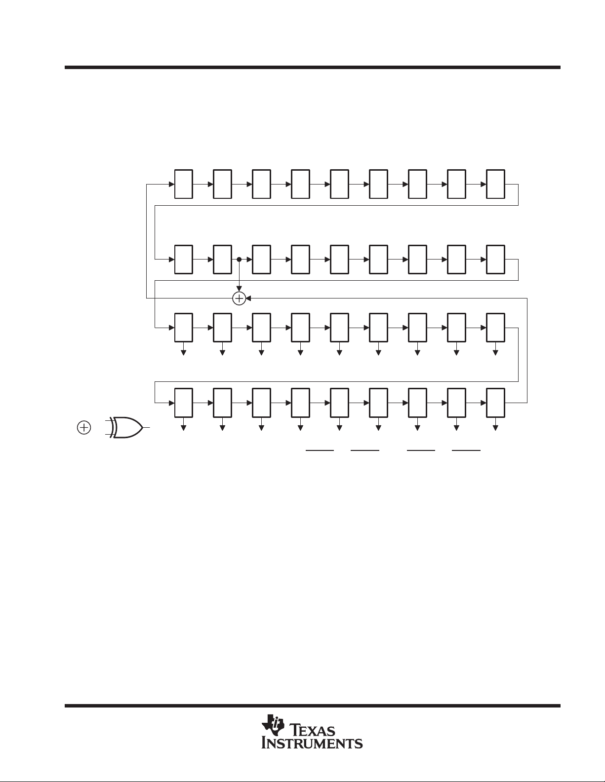
pseudo-random pattern generation (PRPG)
A pseudo-random pattern is generated in the shift-register elements of the selected BSCs on each rising edge
of TCK, updated in the shadow latches, and applied to the associated device output-mode I/O pins on each
falling edge of TCK. Figures 5 and 6 show the 36-bit linear-feedback shift-register algorithms through which the
patterns are generated. An initial seed value should be scanned into the BSR before performing this operation.
A seed value of all zeroes does not produce additional patterns.
2A7-I/O 2A6-I/O 2A5-I/O 2A4-I/O 2A3-I/O 2A2-I/O 2A1-I/O2A8-I/O2A9-I/O
1A7-I/O 1A6-I/O 1A5-I/O 1A4-I/O 1A3-I/O 1A2-I/O 1A1-I/O1A8-I/O1A9-I/O
2B8-I/O 2B7-I/O 2B6-I/O 2B5-I/O 2B4-I/O 2B3-I/O 2B2-I/O 2B1-I/O2B9-I/O
=
1B8-I/O 1B7-I/O 1B6-I/O 1B5-I/O 1B4-I/O 1B3-I/O 1B2-I/O 1B1-I/O1B9-I/O
Figure 5. 36-Bit PRPG Configuration (1OEAB = 2OEAB = 0, 1OEBA = 2OEBA = 1)
POST OFFICE BOX 655303 • DALLAS, TEXAS 75265
15

SN54LVTH18512, SN54LVTH182512, SN74LVTH18512, SN74LVTH182512
3.3-V ABT SCAN TEST DEVICES
WITH 18-BIT UNIVERSAL BUS TRANSCEIVERS
SCBS671B – AUGUST 1996 – REVISED OCTOBER 1997
2B7-I/O 2B6-I/O 2B5-I/O 2B4-I/O 2B3-I/O 2B2-I/O 2B1-I/O2B8-I/O2B9-I/O
1B7-I/O 1B6-I/O 1B5-I/O 1B4-I/O 1B3-I/O 1B2-I/O 1B1-I/O1B8-I/O1B9-I/O
2A8-I/O 2A7-I/O 2A6-I/O 2A5-I/O 2A4-I/O 2A3-I/O 2A2-I/O 2A1-I/O2A9-I/O
=
1A8-I/O 1A7-I/O 1A6-I/O 1A5-I/O 1A4-I/O 1A3-I/O 1A2-I/O 1A1-I/O1A9-I/O
Figure 6. 36-Bit PRPG Configuration (1OEAB = 2OEAB = 1, 1OEBA = 2OEBA = 0)
16
POST OFFICE BOX 655303 • DALLAS, TEXAS 75265

SN54LVTH18512, SN54LVTH182512, SN74LVTH18512, SN74LVTH182512
3.3-V ABT SCAN TEST DEVICES
WITH 18-BIT UNIVERSAL BUS TRANSCEIVERS
SCBS671B – AUGUST 1996 – REVISED OCTOBER 1997
parallel-signature analysis (PSA)
Data appearing at the selected device input-mode I/O pins is compressed into a 36-bit parallel signature in the
shift-register elements of the selected BSCs on each rising edge of TCK. Data in the shadow latches of the
selected output-mode BSCs remains constant and is applied to the associated device I/O pins. Figures 7 and 8
show the 36-bit linear-feedback shift-register algorithms through which the signature is generated. An initial
seed value should be scanned into the BSR before performing this operation.
2A7-I/O 2A6-I/O 2A5-I/O 2A4-I/O 2A3-I/O 2A2-I/O 2A1-I/O2A8-I/O2A9-I/O
1A7-I/O 1A6-I/O 1A5-I/O 1A4-I/O 1A3-I/O 1A2-I/O 1A1-I/O1A8-I/O1A9-I/O
2B8-I/O 2B7-I/O 2B6-I/O 2B5-I/O 2B4-I/O 2B3-I/O 2B2-I/O 2B1-I/O2B9-I/O
=
=
1B8-I/O 1B7-I/O 1B6-I/O 1B5-I/O 1B4-I/O 1B3-I/O 1B2-I/O 1B1-I/O1B9-I/O
Figure 7. 36-Bit PSA Configuration (1OEAB = 2OEAB = 0, 1OEBA = 2OEBA = 1)
POST OFFICE BOX 655303 • DALLAS, TEXAS 75265
17

SN54LVTH18512, SN54LVTH182512, SN74LVTH18512, SN74LVTH182512
3.3-V ABT SCAN TEST DEVICES
WITH 18-BIT UNIVERSAL BUS TRANSCEIVERS
SCBS671B – AUGUST 1996 – REVISED OCTOBER 1997
2B7-I/O 2B6-I/O 2B5-I/O 2B4-I/O 2B3-I/O 2B2-I/O 2B1-I/O2B8-I/O2B9-I/O
1B7-I/O 1B6-I/O 1B5-I/O 1B4-I/O 1B3-I/O 1B2-I/O 1B1-I/O1B8-I/O1B9-I/O
2A8-I/O 2A7-I/O 2A6-I/O 2A5-I/O 2A4-I/O 2A3-I/O 2A2-I/O 2A1-I/O2A9-I/O
=
=
1A8-I/O 1A7-I/O 1A6-I/O 1A5-I/O 1A4-I/O 1A3-I/O 1A2-I/O 1A1-I/O1A9-I/O
Figure 8. 36-Bit PSA Configuration (1OEAB = 2OEAB = 1, 1OEBA = 2OEBA = 0)
18
POST OFFICE BOX 655303 • DALLAS, TEXAS 75265

SN54LVTH18512, SN54LVTH182512, SN74LVTH18512, SN74LVTH182512
3.3-V ABT SCAN TEST DEVICES
WITH 18-BIT UNIVERSAL BUS TRANSCEIVERS
SCBS671B – AUGUST 1996 – REVISED OCTOBER 1997
simultaneous PSA and PRPG (PSA/PRPG)
Data appearing at the selected device input-mode I/O pins is compressed into an 18-bit parallel signature in
the shift-register elements of the selected input-mode BSCs on each rising edge of TCK. At the same time, an
18-bit pseudo-random pattern is generated in the shift-register elements of the selected output-mode BSCs on
each rising edge of TCK, updated in the shadow latches, and applied to the associated device I/O pins on each
falling edge of TCK. Figures 9 and 10 show the 18-bit linear-feedback shift-register algorithms through which
the signature and patterns are generated. An initial seed value should be scanned into the BSR before
performing this operation. A seed value of all zeroes does not produce additional patterns.
2A7-I/O 2A6-I/O 2A5-I/O 2A4-I/O 2A3-I/O 2A2-I/O 2A1-I/O2A8-I/O2A9-I/O
1A7-I/O 1A6-I/O 1A5-I/O 1A4-I/O 1A3-I/O 1A2-I/O 1A1-I/O1A8-I/O1A9-I/O
2B8-I/O 2B7-I/O 2B6-I/O 2B5-I/O 2B4-I/O 2B3-I/O 2B2-I/O 2B1-I/O2B9-I/O
=
=
1B8-I/O 1B7-I/O 1B6-I/O 1B5-I/O 1B4-I/O 1B3-I/O 1B2-I/O 1B1-I/O1B9-I/O
Figure 9. 18-Bit PSA/PRPG Configuration (1OEAB = 2OEAB = 0, 1OEBA = 2OEBA = 1)
POST OFFICE BOX 655303 • DALLAS, TEXAS 75265
19

SN54LVTH18512, SN54LVTH182512, SN74LVTH18512, SN74LVTH182512
3.3-V ABT SCAN TEST DEVICES
WITH 18-BIT UNIVERSAL BUS TRANSCEIVERS
SCBS671B – AUGUST 1996 – REVISED OCTOBER 1997
2B7-I/O 2B6-I/O 2B5-I/O 2B4-I/O 2B3-I/O 2B2-I/O 2B1-I/O2B8-I/O2B9-I/O
1B7-I/O 1B6-I/O 1B5-I/O 1B4-I/O 1B3-I/O 1B2-I/O 1B1-I/O1B8-I/O1B9-I/O
2A8-I/O 2A7-I/O 2A6-I/O 2A5-I/O 2A4-I/O 2A3-I/O 2A2-I/O 2A1-I/O2A9-I/O
=
=
1A8-I/O 1A7-I/O 1A6-I/O 1A5-I/O 1A4-I/O 1A3-I/O 1A2-I/O 1A1-I/O1A9-I/O
Figure 10. 18-Bit PSA/PRPG Configuration (1OEAB = 2OEAB = 1, 1OEBA = 2OEBA = 0)
20
POST OFFICE BOX 655303 • DALLAS, TEXAS 75265

SN54LVTH18512, SN54LVTH182512, SN74LVTH18512, SN74LVTH182512
3.3-V ABT SCAN TEST DEVICES
WITH 18-BIT UNIVERSAL BUS TRANSCEIVERS
SCBS671B – AUGUST 1996 – REVISED OCTOBER 1997
simultaneous PSA and binary count up (PSA/COUNT)
Data appearing at the selected device input-mode I/O pins is compressed into an 18-bit parallel signature in
the shift-register elements of the selected input-mode BSCs on each rising edge of TCK. At the same time, an
18-bit binary count-up pattern is generated in the shift-register elements of the selected output-mode BSCs on
each rising edge of TCK, updated in the shadow latches, and applied to the associated device I/O pins on each
falling edge of TCK. Figures 1 1 and 12 show the 18-bit linear-feedback shift-register algorithms through which
the signature is generated. An initial seed value should be scanned into the BSR before performing
this operation.
2A7-I/O 2A6-I/O 2A5-I/O 2A4-I/O 2A3-I/O 2A2-I/O 2A1-I/O2A8-I/O2A9-I/O
1A7-I/O 1A6-I/O 1A5-I/O 1A4-I/O 1A3-I/O 1A2-I/O 1A1-I/O1A8-I/O1A9-I/O
MSB
2B8-I/O 2B7-I/O 2B6-I/O 2B5-I/O 2B4-I/O 2B3-I/O 2B2-I/O 2B1-I/O2B9-I/O
LSB
=
=
1B8-I/O 1B7-I/O 1B6-I/O 1B5-I/O 1B4-I/O 1B3-I/O 1B2-I/O 1B1-I/O1B9-I/O
Figure 11. 18-Bit PSA/COUNT Configuration (1OEAB = 2OEAB = 0, 1OEBA = 2OEBA = 1)
POST OFFICE BOX 655303 • DALLAS, TEXAS 75265
21

SN54LVTH18512, SN54LVTH182512, SN74LVTH18512, SN74LVTH182512
3.3-V ABT SCAN TEST DEVICES
WITH 18-BIT UNIVERSAL BUS TRANSCEIVERS
SCBS671B – AUGUST 1996 – REVISED OCTOBER 1997
2B7-I/O 2B6-I/O 2B5-I/O 2B4-I/O 2B3-I/O 2B2-I/O 2B1-I/O2B8-I/O2B9-I/O
1B9-I/O
MSB
2A8-I/O 2A7-I/O 2A6-I/O 2A5-I/O 2A4-I/O 2A3-I/O 2A2-I/O 2A1-I/O2A9-I/O
=
=
1A8-I/O 1A7-I/O 1A6-I/O 1A5-I/O 1A4-I/O 1A3-I/O 1A2-I/O 1A1-I/O1A9-I/O
1B7-I/O 1B6-I/O 1B5-I/O 1B4-I/O 1B3-I/O 1B2-I/O 1B1-I/O1B8-I/O
LSB
Figure 12. 18-Bit PSA/COUNT Configuration (1OEAB = 2OEAB = 1, 1OEBA = 2OEBA = 0)
22
POST OFFICE BOX 655303 • DALLAS, TEXAS 75265

SN54LVTH18512, SN54LVTH182512, SN74LVTH18512, SN74LVTH182512
3.3-V ABT SCAN TEST DEVICES
WITH 18-BIT UNIVERSAL BUS TRANSCEIVERS
SCBS671B – AUGUST 1996 – REVISED OCTOBER 1997
timing description
All test operations of the ’L VTH18512 and ’LVTH182512 are synchronous to the TCK signal. Data on the TDI,
TMS, and normal-function inputs is captured on the rising edge of TCK. Data appears on the TDO and
normal-function output pins on the falling edge of TCK. The T AP controller is advanced through its states (as
shown in Figure 1) by changing the value of TMS on the falling edge of TCK and then applying a rising edge
to TCK.
A simple timing example is shown in Figure 13. In this example, the TAP controller begins in the
Test-Logic-Reset state and is advanced through its states, as necessary, to perform one instruction-register
scan and one data-register scan. While in the Shift-IR and Shift-DR states, TDI is used to input serial data, and
TDO is used to output serial data. The TAP controller is then returned to the Test-Logic-Reset state. Table 5
details the operation of the test circuitry during each TCK cycle.
Table 5. Explanation of Timing Example
TCK
CYCLE(S)
1 Test-Logic-Reset
2 Run-Test/Idle
3 Select-DR-Scan
4 Select-IR-Scan
5 Capture-IR
6 Shift-IR
7–13 Shift-IR
14 Exit1-IR TDO becomes inactive (goes to the high-impedance state) on the falling edge of TCK.
15 Update-IR The IR is updated with the new instruction (BYPASS) on the falling edge of TCK.
16 Select-DR-Scan
17 Capture-DR
18 Shift-DR
19–20 Shift-DR The binary value 101 is shifted in via TDI, while the binary value 010 is shifted out via TDO.
21 Exit1-DR TDO becomes inactive (goes to the high-impedance state) on the falling edge of TCK.
22 Update-DR The selected data register is updated with the new data on the falling edge of TCK.
23 Select-DR-Scan
24 Select-IR-Scan
25 Test-Logic-Reset Test operation completed
TAP STATE
AFTER TCK
DESCRIPTION
TMS is changed to a logic 0 value on the falling edge of TCK to begin advancing the TAP controller toward
the desired state.
The IR captures the 8-bit binary value 10000001 on the rising edge of TCK as the TAP controller exits the
Capture-IR state.
TDO becomes active and TDI is made valid on the falling edge of TCK. The first bit is shifted into the TAP
on the rising edge of TCK as the TAP controller advances to the next state.
One bit is shifted into the IR on each TCK rising edge. With TDI held at a logic 1 value, the 8-bit binary value
11111111 is serially scanned into the IR. At the same time, the 8-bit binary value 10000001 is serially scanned
out of the IR via TDO. In TCK cycle 13, TMS is changed to a logic 1 value to end the IR scan on the next
TCK cycle. The last bit of the instruction is shifted as the TAP controller advances from Shift-IR to Exit1-IR.
The bypass register captures a logic 0 value on the rising edge of TCK as the TAP controller exits the
Capture-DR state.
TDO becomes active and TDI is made valid on the falling edge of TCK. The first bit is shifted into the TAP
on the rising edge of TCK as the TAP controller advances to the next state.
POST OFFICE BOX 655303 • DALLAS, TEXAS 75265
23

SN54LVTH18512, SN54LVTH182512, SN74LVTH18512, SN74LVTH182512
3.3-V ABT SCAN TEST DEVICES
WITH 18-BIT UNIVERSAL BUS TRANSCEIVERS
SCBS671B – AUGUST 1996 – REVISED OCTOBER 1997
1 2 3 4 5 6 7 8 9 10 11 12 13 14 15 16 17 18 19 20 21 22 23 24 25
TCK
TMS
TDI
TDO
TAP
Controller
State
Run-Test/Idle
Test-Logic-Reset
Select-DR-Scan
Capture-IR
Select-IR-Scan
Shift-IR
3-State (TDO) or Don’t Care (TDI)
Exit1-IR
Update-IR
Capture-DR
Select-DR-Scan
Shift-DR
Exit1-DR
Update-DR
Select-IR-Scan
Select-DR-Scan
Figure 13. Timing Example
absolute maximum ratings over operating free-air temperature range (unless otherwise noted)
Supply voltage range, VCC –0.5 V to 4.6 V. . . . . . . . . . . . . . . . . . . . . . . . . . . . . . . . . . . . . . . . . . . . . . . . . . . . . . . . .
Input voltage range, VI (see Note 1) –0.5 V to 7 V. . . . . . . . . . . . . . . . . . . . . . . . . . . . . . . . . . . . . . . . . . . . . . . . . .
Voltage range applied to any output in the high or power-off state, V
Current into any output in the low state, I
: SN54LVTH18512 96 mA. . . . . . . . . . . . . . . . . . . . . . . . . . . . . . . . . .
O
SN54LVTH182512 (A port or TDO) 96 mA. . . . . . . . . . . . . . . . . .
SN54LVTH182512 (B port) 30 mA. . . . . . . . . . . . . . . . . . . . . . . . .
SN74LVTH18512 128 mA. . . . . . . . . . . . . . . . . . . . . . . . . . . . . . . . .
SN74LVTH182512 (A port or TDO) 128 mA. . . . . . . . . . . . . . . . .
SN74LVTH182512 (B port) 30 mA. . . . . . . . . . . . . . . . . . . . . . . . .
Current into any output in the high state, I
(see Note 2): SN54LVTH18512 48 mA. . . . . . . . . . . . . . . . . . . . .
O
SN54LVTH182512 (A port or TDO) 48 mA. . . . . .
SN54LVTH182512 (B port) 30 mA. . . . . . . . . . . . .
SN74LVTH18512 64 mA. . . . . . . . . . . . . . . . . . . . .
SN74LVTH182512 (A port or TDO) 64 mA. . . . . .
SN74LVTH182512 (B port) 30 mA. . . . . . . . . . . . .
Input clamp current, I
Output clamp current, I
Package thermal impedance,
Storage temperature range, T
†
Stresses beyond those listed under “absolute maximum ratings” may cause permanent damage to the device. These are stress ratings only, and
functional operation of the device at these or any other conditions beyond those indicated under “recommended operating conditions” is not
implied. Exposure to absolute-maximum-rated conditions for extended periods may affect device reliability.
NOTES: 1. The input and output negative-voltage ratings can be exceeded if the input and output clamp-current ratings are observed.
2. This current only flows when the output is in the high state and VO > VCC.
3. The package thermal impedance is calculated in accordance with JESD 51.
(V
< 0) –50 mA. . . . . . . . . . . . . . . . . . . . . . . . . . . . . . . . . . . . . . . . . . . . . . . . . . . . . . . . . . .
IK
I
(V
< 0) –50 mA. . . . . . . . . . . . . . . . . . . . . . . . . . . . . . . . . . . . . . . . . . . . . . . . . . . . . . . .
OK
O
qJA (see Note 3): DGG package 73°C/W. . . . . . . . . . . . . . . . . . . . . . . . . . . . . . .
–65°C to 150°C. . . . . . . . . . . . . . . . . . . . . . . . . . . . . . . . . . . . . . . . . . . . . . . . . . .
stg
(see Note 1) –0.5 V to 7 V. . . . . . . . .
O
Test-Logic-Reset
†
24
POST OFFICE BOX 655303 • DALLAS, TEXAS 75265

UNIT
SN54LVTH18512, SN54LVTH182512, SN74LVTH18512, SN74LVTH182512
3.3-V ABT SCAN TEST DEVICES
WITH 18-BIT UNIVERSAL BUS TRANSCEIVERS
SCBS671B – AUGUST 1996 – REVISED OCTOBER 1997
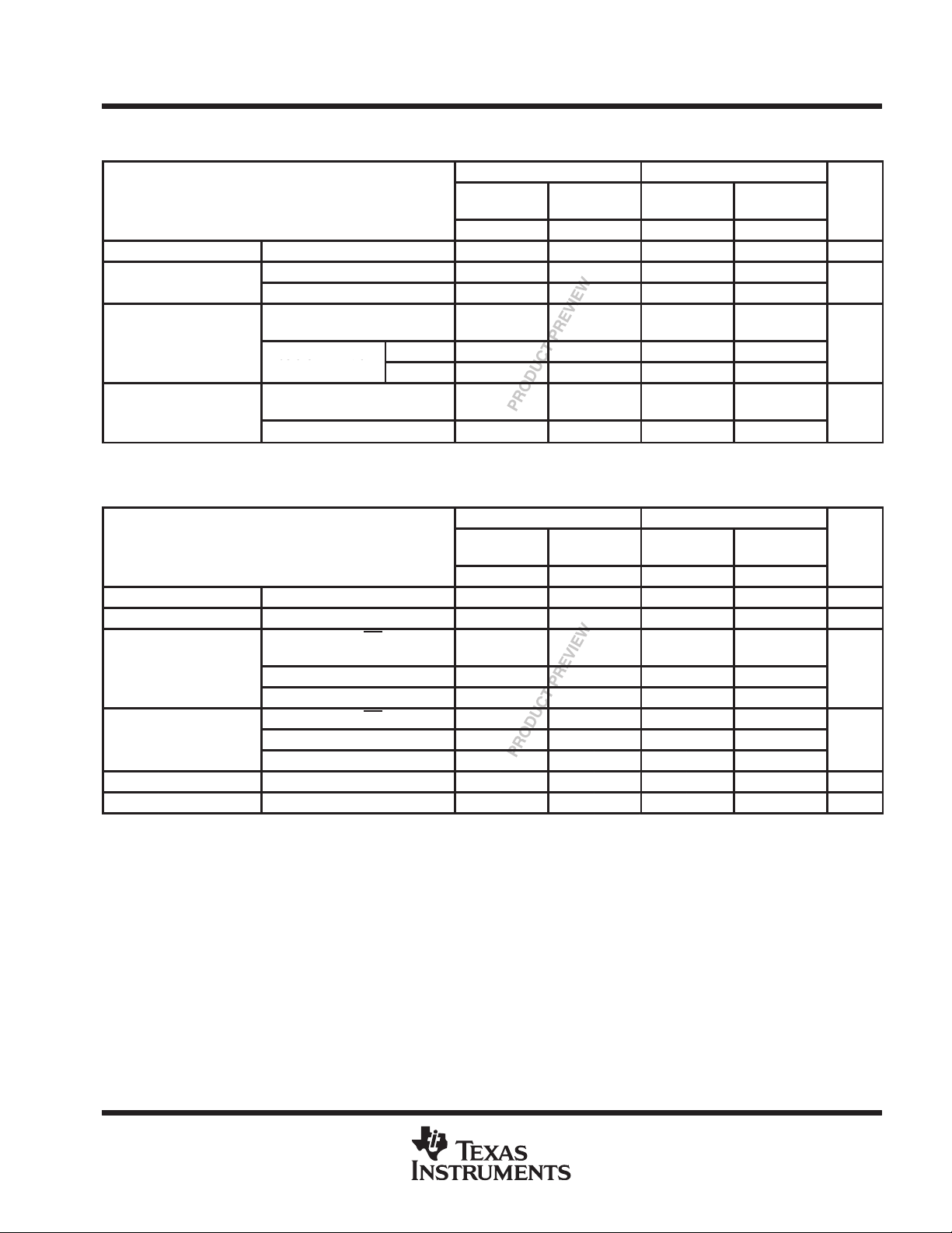
recommended operating conditions (see Note 4)
SN54LVTH18512 SN74LVTH18512
MIN MAX MIN MAX
V
V
V
V
I
OH
I
OL
I
OL
∆t/∆v Input transition rise or fall rate Outputs enabled 10 10 ns/V
T
†
Current duty cycle ≤ 50%, f ≥ 1 kHz
NOTE 4: Unused control inputs must be held high or low to prevent them from floating.
Supply voltage 2.7 3.6 2.7 3.6 V
CC
High-level input voltage 2 2 V
IH
Low-level input voltage 0.8 0.8 V
IL
Input voltage 5.5 5.5 V
I
High-level output current –24 –32 mA
Low-level output current 24 32 mA
†
Low-level output current 48 64 mA
Operating free-air temperature –55 125 –40 85 °C
A
PRODUCT PREVIEW information concerns products in the formative or
design phase of development. Characteristic data and other
specifications are design goals. Texas Instruments reserves the right to
change or discontinue these products without notice.
POST OFFICE BOX 655303 • DALLAS, TEXAS 75265
25

SN54LVTH18512, SN54LVTH182512, SN74LVTH18512, SN74LVTH182512
PARAMETER
TEST CONDITIONS
UNIT
V
V
V
V
V
3 V
,
CLK,
I
TDI, TMS
A
‡
orts
‡
I
§
V
V
A
V
CC
3.3-V ABT SCAN TEST DEVICES
WITH 18-BIT UNIVERSAL BUS TRANSCEIVERS
SCBS671B – AUGUST 1996 – REVISED OCTOBER 1997
electrical characteristics over recommended operating free-air temperature range (unless
otherwise noted)
SN54LVTH18512 SN74LVTH18512
MIN TYP†MAX MIN TYP†MAX
V
IK
V
OH
OL
CLK
LE, TCK
OE,
I
A or B
p
I
off
I(hold)
I
OZH
I
OZL
I
OZPU
I
OZPD
I
CC
∆I
CC
C
i
C
io
C
o
†
All typical values are at VCC = 3.3 V, TA = 25°C.
‡
Unused pins at VCC or GND
§
The parameter I
¶
This is the increase in supply current for each input that is at the specified TTL voltage level rather than VCC or GND.
A or B
ports
TDO VCC = 3.6 V, VO = 3 V 1 1 µA
TDO VCC = 3.6 V, VO = 0.5 V –1 –1 µA
TDO VCC = 0 to 1.5 V, VO = 0.5 V or 3 V ±50 ±50 µA
TDO VCC = 1.5 V to 0, VO = 0.5 V or 3 V ±50 ±50 µA
¶
I(hold)
VCC = 2.7 V, II = –18 mA –1.2 –1.2 V
VCC = 2.7 V to 3.6 V, IOH = –100 µA VCC–0.2 VCC–0.2
VCC = 2.7 V, IOH = –3 mA 2.4 2.4
IOH = –8 mA 2.4 2.4
VCC = 3 V
= 2.7
CC
=
CC
VCC = 3.6 V, VI = VCC or GND ±1 ±1
VCC = 0 or 3.6 V, VI = 5.5 V 10 10
VCC = 3.6 V
VCC = 3.6 V
VCC = 0, VI or VO = 0 to 4.5 V ±100 µA
= 3
CC
=
= 3.6 V,
IO = 0,
VI = VCC or GND
VCC = 3 V to 3.6 V, One input at VCC – 0.6 V,
Other inputs at VCC or GND
VI = 3 V or 0 4 4 pF
VO = 3 V or 0 10 10 pF
VO = 3 V or 0 8 8 pF
includes the off-state output leakage current.
IOH = –24 mA 2
IOH = –32 mA 2
IOL = 100 µA 0.2 0.2
IOL = 24 mA 0.5 0.5
IOL = 16 mA 0.4 0.4
IOL = 32 mA 0.5 0.5
IOL = 48 mA 0.55
IOL = 64 mA 0.55
VI = 5.5 V 5 5
VI = V
CC
VI = 0 –25 –100 –25 –100
VI = 5.5 V 20 20
VI = V
CC
VI = 0 –5 –5
VI = 0.8 V 75 500 75 150 500
VI = 2 V –75 –500 –75 –150 –500
Outputs high 0.6 2 0.6 2
Outputs low 18 24 18 24
Outputs disabled 0.6 2 0.6 2
1 1
1 1
0.5 0.5 mA
V
µ
µ
mA
PRODUCT PREVIEW information concerns products in the formative or
design phase of development. Characteristic data and other
specifications are design goals. Texas Instruments reserves the right to
change or discontinue these products without notice.
26
POST OFFICE BOX 655303 • DALLAS, TEXAS 75265
twPulse duration
ns
A before LEAB↓ or
h
SN54LVTH18512, SN54LVTH182512, SN74LVTH18512, SN74LVTH182512
3.3-V ABT SCAN TEST DEVICES
WITH 18-BIT UNIVERSAL BUS TRANSCEIVERS
SCBS671B – AUGUST 1996 – REVISED OCTOBER 1997
timing requirements over recommended operating free-air temperature range (unless otherwise
noted) (normal mode) (see Figure 14)
SN54LVTH18512 SN74LVTH18512
f
clock
t
su
t
VCC = 3.3 V
± 0.3 V
MIN MAX MIN MAX MIN MAX MIN MAX
Clock frequency CLKAB or CLKBA 0 100 0 80 0 100 0 80 MHz
CLKAB or CLKBA high or low 4.4 5.6 4.4 5.6
LEAB or LEBA high 3 3 3 3
Setup time
Hold time
A before CLKAB↑ or
B before CLKBA↑
A before LEAB↓ or
B before LEBA↓
A after CLKAB↑ or
B after CLKBA↑
A after LEAB↓ or B after LEBA↓ 3.1 3.5 3.1 3.5
CLK high 1.5 0.7 1.5 0.7
CLK low 1.6 1.6 1.6 1.6
2.8 3 2.8 3
1.4 1.1 1.4 1.1
VCC = 2.7 V
timing requirements over recommended operating free-air temperature range (unless otherwise
noted) (test mode) (see Figure 14)
SN54LVTH18512 SN74LVTH18512
f
clock
t
w
t
su
t
h
t
d
t
r
VCC = 3.3 V
± 0.3 V
MIN MAX MIN MAX MIN MAX MIN MAX
Clock frequency TCK 0 50 0 40 0 50 0 40 MHz
Pulse duration TCK high or low 9.5 10.5 9.5 10.5 ns
A, B, CLK, LE, or OE
Setup time
Hold time
Delay time Power up to TCK↑ 50 50 50 50 ns
Rise time VCC power up 1 1 1 1 µs
before TCK↑
TDI before TCK↑
TMS before TCK↑ 2.5 3.5 2.5 3.5
A, B, CLK, LE, or OE after TCK↑ 1.7 1 1.7 1
TDI after TCK↑
TMS after TCK↑ 1.5 1 1.5 1
6.5 7 6.5 7
2.5 3.5 2.5 3.5
1.5 1 1.5 1
VCC = 2.7 V
VCC = 3.3 V
± 0.3 V
VCC = 3.3 V
± 0.3 V
VCC = 2.7 V
VCC = 2.7 V
UNIT
ns
ns
UNIT
ns
ns
PRODUCT PREVIEW information concerns products in the formative or
design phase of development. Characteristic data and other
specifications are design goals. Texas Instruments reserves the right to
change or discontinue these products without notice.
POST OFFICE BOX 655303 • DALLAS, TEXAS 75265
27

SN54LVTH18512, SN54LVTH182512, SN74LVTH18512, SN74LVTH182512
A or B
B or A
ns
CLKAB or CLKBA
B or A
ns
LEAB or LEBA
B or A
ns
OEAB
OEBA
B or A
ns
OEAB
OEBA
B or A
ns
TCK↓
A or B
ns
TCK↓
TDO
ns
TCK↓
A or B
ns
TCK↓
TDO
ns
TCK↓
A or B
ns
TCK↓
TDO
ns
3.3-V ABT SCAN TEST DEVICES
WITH 18-BIT UNIVERSAL BUS TRANSCEIVERS
SCBS671B – AUGUST 1996 – REVISED OCTOBER 1997
switching characteristics over recommended operating free-air temperature range (unless
otherwise noted) (normal mode) (see Figure 14)
SN54LVTH18512 SN74LVTH18512
PARAMETER
f
max
t
PLH
t
PHL
t
PLH
t
PHL
t
PLH
t
PHL
t
PZH
t
PZL
t
PHZ
t
PLZ
FROM
(INPUT)
CLKAB or CLKBA 100 80 100 80 MHz
or
or
TO
(OUTPUT)
VCC = 3.3 V
± 0.3 V
MIN MAX MIN MAX MIN MAX MIN MAX
1.5 5.1 5.8 1.5 4.9 5.6
1.5 5.1 5.8 1.5 4.9 5.6
1.5 6.3 7.2 1.5 5.8 6.8
1.5 6.3 7.2 1.5 5.8 6.8
1.5 7.8 9.2 1.5 7.4 8.4
1.5 6 6.6 1.5 5.7 6.4
1.5 7.6 8.5 1.5 7.1 8.3
1.5 7.6 8.5 1.5 7.1 8.3
2.5 8.3 8.8 2.5 7.8 8.4
2.5 8.3 8.8 2.5 7.8 8.4
VCC = 2.7 V
VCC = 3.3 V
± 0.3 V
VCC = 2.7 V
UNIT
switching characteristics over recommended operating free-air temperature range (unless
otherwise noted) (test mode) (see Figure 14)
SN54LVTH18512 SN74LVTH18512
PARAMETER
f
max
t
PLH
t
PHL
t
PLH
t
PHL
t
PZH
t
PZL
t
PZH
t
PZL
t
PHZ
t
PLZ
t
PHZ
t
PLZ
FROM
(INPUT)
TCK 50 40 50 40 MHz
TO
(OUTPUT)
VCC = 3.3 V
± 0.3 V
MIN MAX MIN MAX MIN MAX MIN MAX
2.5 15 18 2.5 14 17
2.5 15 18 2.5 14 17
1 6 7 1 5.5 6.5
1.5 7 8 1.5 6.5 7.5
4 18 21 4 17 20
4 18 21 4 17 20
1 6 7 1 5.5 6.5
1.5 6 7 1.5 5.5 6.5
4 19 21 4 18 20
4 18 19.5 4 17 18.5
1.5 7.5 9 1.5 7 8.5
1.5 7.5 8.5 1.5 7 8
VCC = 2.7 V
VCC = 3.3 V
± 0.3 V
VCC = 2.7 V
UNIT
PRODUCT PREVIEW information concerns products in the formative or
design phase of development. Characteristic data and other
specifications are design goals. Texas Instruments reserves the right to
change or discontinue these products without notice.
28
POST OFFICE BOX 655303 • DALLAS, TEXAS 75265
UNIT
IOHHigh-level output current
mA
IOLLow-level output current
mA
SN54LVTH18512, SN54LVTH182512, SN74LVTH18512, SN74LVTH182512
3.3-V ABT SCAN TEST DEVICES
WITH 18-BIT UNIVERSAL BUS TRANSCEIVERS
SCBS671B – AUGUST 1996 – REVISED OCTOBER 1997
recommended operating conditions (see Note 4)
SN54LVTH182512 SN74LVTH182512
MIN MAX MIN MAX
V
V
V
V
I
OL
∆t/∆v Input transition rise or fall rate Outputs enabled 10 10 ns/V
T
†
Current duty cycle ≤ 50%, f ≥ 1 kHz
NOTE 4: Unused control inputs must be held high or low to prevent them from floating.
Supply voltage 2.7 3.6 2.7 3.6 V
CC
High-level input voltage 2 2 V
IH
Low-level input voltage 0.8 0.8 V
IL
Input voltage 5.5 5.5 V
I
p
p
†
Low-level output current A port, TDO 48 64 mA
Operating free-air temperature –55 125 –40 85 °C
A
A port, TDO –24 –32
B port –12 –12
A port, TDO 24 32
B port 12 12
PRODUCT PREVIEW information concerns products in the formative or
design phase of development. Characteristic data and other
specifications are design goals. Texas Instruments reserves the right to
change or discontinue these products without notice.
POST OFFICE BOX 655303 • DALLAS, TEXAS 75265
29
SN54LVTH18512, SN54LVTH182512, SN74LVTH18512, SN74LVTH182512
PARAMETER
TEST CONDITIONS
UNIT
V
,
V
TDO
V
V
,
CLK,
I
TDI, TMS
A
‡
orts
‡
I
§
V
V
A
V
CC
3.3-V ABT SCAN TEST DEVICES
WITH 18-BIT UNIVERSAL BUS TRANSCEIVERS
SCBS671B – AUGUST 1996 – REVISED OCTOBER 1997
electrical characteristics over recommended operating free-air temperature range (unless
otherwise noted)
SN54LVTH182512 SN74LVTH182512
MIN TYP†MAX MIN TYP†MAX
V
IK
A, B, TDO VCC = 2.7 V to 3.6 V, IOH = –100 µA VCC–0.2 VCC–0.2
OH
V
OL
I
I
off
I(hold)
I
OZH
I
OZL
I
OZPU
I
OZPD
I
CC
∆I
CC
C
i
C
io
C
o
†
All typical values are at VCC = 3.3 V, TA = 25°C.
‡
Unused pins at VCC or GND
§
The parameter I
¶
This is the increase in supply current for each input that is at the specified TTL voltage level rather than VCC or GND.
A port,
TDO
B port VCC = 3 V, IOH = –12 mA 2 2
A, B, TDO VCC = 2.7 V, IOL = 100 µA 0.2 0.2
A port,
B port VCC = 3 V, IOL = 12 mA 0.8 0.8
CLK
LE, TCK
OE,
A or B
p
A or B
ports
TDO VCC = 3.6 V, VO = 3 V 1 1 µA
TDO VCC = 3.6 V, VO = 0.5 V –1 –1 µA
TDO VCC = 0 to 1.5 V, VO = 0.5 V or 3 V ±50 ±50 µA
TDO VCC = 1.5 V to 0, VO = 0.5 V or 3 V ±50 ±50 µA
¶
I(hold)
VCC = 2.7 V, II = –18 mA –1.2 –1.2 V
VCC = 2.7 V, IOH = –3 mA 2.4 2.4
IOH = –8 mA 2.4 2.4
VCC = 3 V
VCC = 2.7 V, IOL = 24 mA 0.5 0.5
= 3
CC
VCC = 3.6 V, VI = VCC or GND ±1 ±1
VCC = 0 or 3.6 V, VI = 5.5 V 10 10
VCC = 3.6 V
VCC = 3.6 V
VCC = 0, VI or VO = 0 to 4.5 V ±100 µA
= 3
CC
=
= 3.6 V,
IO = 0,
VI = VCC or GND
VCC = 3 V to 3.6 V, One input at VCC – 0.6 V,
Other inputs at VCC or GND
VI = 3 V or 0 4 4 pF
VO = 3 V or 0 10 10 pF
VO = 3 V or 0 8 8 pF
includes the off-state output leakage current.
IOH = –24 mA 2
IOH = –32 mA 2
IOL = 16 mA 0.4 0.4
IOL = 32 mA 0.5 0.5
IOL = 48 mA 0.55
IOL = 64 mA 0.55
VI = 5.5 V 5 5
VI = V
CC
VI = 0 –25 –100 –25 –100
VI = 5.5 V 20 20
VI = V
CC
VI = 0 –5 –5
VI = 0.8 V 75 500 75 150 500
VI = 2 V –75 –500 –75 –150 –500
Outputs high 0.6 2 0.6 2
Outputs low 18 24 18 24
Outputs disabled 0.6 2 0.6 2
1 1
1 1
0.5 0.5 mA
V
µ
µ
mA
PRODUCT PREVIEW information concerns products in the formative or
design phase of development. Characteristic data and other
specifications are design goals. Texas Instruments reserves the right to
change or discontinue these products without notice.
30
POST OFFICE BOX 655303 • DALLAS, TEXAS 75265

twPulse duration
ns
A before LEAB↓ or
h
SN54LVTH18512, SN54LVTH182512, SN74LVTH18512, SN74LVTH182512
3.3-V ABT SCAN TEST DEVICES
WITH 18-BIT UNIVERSAL BUS TRANSCEIVERS
SCBS671B – AUGUST 1996 – REVISED OCTOBER 1997
timing requirements over recommended operating free-air temperature range (unless otherwise
noted) (normal mode) (see Figure 14)
SN54LVTH182512 SN74LVTH182512
f
clock
t
su
t
VCC = 3.3 V
± 0.3 V
MIN MAX MIN MAX MIN MAX MIN MAX
Clock frequency CLKAB or CLKBA 0 100 0 80 0 100 0 80 MHz
CLKAB or CLKBA high or low 4.4 5.6 4.4 5.6
LEAB or LEBA high 3 3 3 3
Setup time
Hold time
A before CLKAB↑ or
B before CLKBA↑
A before LEAB↓ or
B before LEBA↓
A after CLKAB↑ or
B after CLKBA↑
A after LEAB↓ or B after LEBA↓ 3.1 3.5 3.1 3.5
CLK high 1.5 0.7 1.5 0.7
CLK low 1.6 1.6 1.6 1.6
2.8 3 2.8 3
1.4 1.1 1.4 1.1
VCC = 2.7 V
timing requirements over recommended operating free-air temperature range (unless otherwise
noted) (test mode) (see Figure 14)
SN54LVTH182512 SN74LVTH182512
f
clock
t
w
t
su
t
h
t
d
t
r
VCC = 3.3 V
± 0.3 V
MIN MAX MIN MAX MIN MAX MIN MAX
Clock frequency TCK 0 50 0 40 0 50 0 40 MHz
Pulse duration TCK high or low 9.5 10.5 9.5 10.5 ns
A, B, CLK, LE, or OE
Setup time
Hold time
Delay time Power up to TCK↑ 50 50 50 50 ns
Rise time VCC power up 1 1 1 1 µs
before TCK↑
TDI before TCK↑
TMS before TCK↑ 2.5 3.5 2.5 3.5
A, B, CLK, LE, or OE after TCK↑ 1.7 1 1.7 1
TDI after TCK↑
TMS after TCK↑ 1.5 1 1.5 1
6.5 7 6.5 7
2.5 3.5 2.5 3.5
1.5 1 1.5 1
VCC = 2.7 V
VCC = 3.3 V
± 0.3 V
VCC = 3.3 V
± 0.3 V
VCC = 2.7 V
VCC = 2.7 V
UNIT
ns
ns
UNIT
ns
ns
PRODUCT PREVIEW information concerns products in the formative or
design phase of development. Characteristic data and other
specifications are design goals. Texas Instruments reserves the right to
change or discontinue these products without notice.
POST OFFICE BOX 655303 • DALLAS, TEXAS 75265
31

SN54LVTH18512, SN54LVTH182512, SN74LVTH18512, SN74LVTH182512
A
B
ns
B
A
ns
CLKAB
B
ns
CLKBA
A
ns
LEAB
B
ns
LEBA
A
ns
OEAB
OEBA
B or A
ns
OEAB
OEBA
B or A
ns
TCK↓
A or B
ns
TCK↓
TDO
ns
TCK↓
A or B
ns
TCK↓
TDO
ns
TCK↓
A or B
ns
TCK↓
TDO
ns
3.3-V ABT SCAN TEST DEVICES
WITH 18-BIT UNIVERSAL BUS TRANSCEIVERS
SCBS671B – AUGUST 1996 – REVISED OCTOBER 1997
switching characteristics over recommended operating free-air temperature range (unless
otherwise noted) (normal mode) (see Figure 14)
SN54LVTH182512 SN74LVTH182512
PARAMETER
f
max
t
PLH
t
PHL
t
PLH
t
PHL
t
PLH
t
PHL
t
PLH
t
PHL
t
PLH
t
PHL
t
PLH
t
PHL
t
PZH
t
PZL
t
PHZ
t
PLZ
FROM
(INPUT)
CLKAB or CLKBA 100 80 100 80 MHz
or
or
TO
(OUTPUT)
VCC = 3.3 V
± 0.3 V
MIN MAX MIN MAX MIN MAX MIN MAX
1.5 6 6.7 1.5 5.7 6.4
1.5 6 6.7 1.5 5.7 6.4
1.5 5.1 5.8 1.5 4.9 5.6
1.5 5.1 5.8 1.5 4.9 5.6
1.5 7.1 8.1 1.5 6.7 7.7
1.5 7.1 8.1 1.5 6.7 7.7
1.5 6.3 7.2 1.5 5.8 6.8
1.5 6.3 7.2 1.5 5.8 6.8
1.5 8.7 9.7 1.5 8.2 9.2
1.5 6.5 6.9 1.5 6.2 6.7
1.5 7.8 9.2 1.5 7.4 8.4
1.5 6 6.6 1.5 5.7 6.4
1.5 8.4 9.6 1.5 7.9 8.7
1.5 8.4 9.6 1.5 7.9 8.7
2.5 9.1 9.3 2.5 8.4 8.9
2.5 9.1 9.3 2.5 8.4 8.9
VCC = 2.7 V
VCC = 3.3 V
± 0.3 V
VCC = 2.7 V
UNIT
switching characteristics over recommended operating free-air temperature range (unless
otherwise noted) (test mode) (see Figure 14)
SN54LVTH182512 SN74LVTH182512
PARAMETER
f
max
t
PLH
t
PHL
t
PLH
t
PHL
t
PZH
t
PZL
t
PZH
t
PZL
t
PHZ
t
PLZ
t
PHZ
t
PLZ
FROM
(INPUT)
TCK 50 40 50 40 MHz
TO
(OUTPUT)
VCC = 3.3 V
± 0.3 V
MIN MAX MIN MAX MIN MAX MIN MAX
2.5 15 18 2.5 14 17
2.5 15 18 2.5 14 17
1 6 7 1 5.5 6.5
1.5 7 8 1.5 6.5 7.5
4 18 21 4 17 20
4 18 21 4 17 20
1 6 7 1 5.5 6.5
1.5 6 7 1.5 5.5 6.5
4 19 21 4 18 20
4 18 19.5 4 17 18.5
1.5 7.5 9 1.5 7 8.5
1.5 7.5 8.5 1.5 7 8
VCC = 2.7 V
VCC = 3.3 V
± 0.3 V
VCC = 2.7 V
UNIT
PRODUCT PREVIEW information concerns products in the formative or
design phase of development. Characteristic data and other
specifications are design goals. Texas Instruments reserves the right to
change or discontinue these products without notice.
32
POST OFFICE BOX 655303 • DALLAS, TEXAS 75265

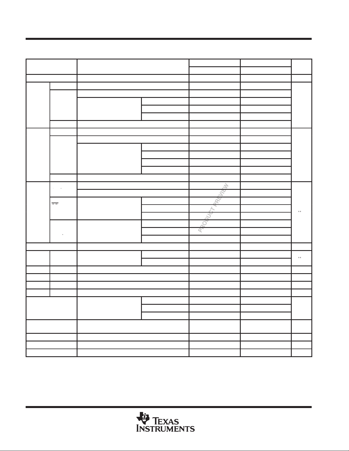
From Output
Under Test
Input
SN54LVTH18512, SN54LVTH182512, SN74LVTH18512, SN74LVTH182512
CL = 50 pF
(see Note A)
1.5 V 1.5 V
VOLTAGE WAVEFORMS
PULSE DURATION
500 Ω
LOAD CIRCUIT
t
w
3.3-V ABT SCAN TEST DEVICES
WITH 18-BIT UNIVERSAL BUS TRANSCEIVERS
SCBS671B – AUGUST 1996 – REVISED OCTOBER 1997
PARAMETER MEASUREMENT INFORMATION
6 V
500 Ω
S1
Open
GND
2.7 V
0 V
Timing Input
Data Input
TEST S1
t
PLH/tPHL
t
PLZ/tPZL
t
PHZ/tPZH
t
1.5 V 1.5 V
VOLTAGE WAVEFORMS
SETUP AND HOLD TIMES
su
Open
GND
1.5 V
t
6 V
2.7 V
0 V
h
2.7 V
0 V
Input
t
PLH
Output
t
PHL
Output
PROPAGATION DELAY TIMES
INVERTING AND NONINVERTING OUTPUTS
NOTES: A. CL includes probe and jig capacitance.
B. Waveform 1 is for an output with internal conditions such that the output is low except when disabled by the output control.
Waveform 2 is for an output with internal conditions such that the output is high except when disabled by the output control.
C. All input pulses are supplied by generators having the following characteristics: PRR ≤ 10 MHz, ZO = 50 Ω, tr ≤ 2.5 ns, tf≤ 2.5 ns.
D. The outputs are measured one at a time with one transition per measurement.
1.5 V 1.5 V
1.5 V
VOLTAGE WAVEFORMS
Figure 14. Load Circuit and Voltage Waveforms
t
PHL
1.5 V
t
PLH
1.5 V1.5 V
2.7 V
0 V
V
OH
V
OL
V
OH
V
OL
Output
Control
Output
Waveform 1
S1 at 6 V
(see Note B)
Output
Waveform 2
S1 at GND
(see Note B)
1.5 V
t
PZL
t
PLZ
1.5 V
t
t
PZH
ENABLE AND DISABLE TIMES
LOW- AND HIGH-LEVEL ENABLING
PHZ
1.5 V
VOLTAGE WAVEFORMS
1.5 V
VOL + 0.3 V
VOH – 0.3 V
2.7 V
0 V
3 V
V
OL
V
OH
≈ 0 V
POST OFFICE BOX 655303 • DALLAS, TEXAS 75265
33

PACKAGE OPTION ADDENDUM
www.ti.com
5-Sep-2005
PACKAGING INFORMATION
Orderable Device Status
(1)
Package
Type
Package
Drawing
Pins Package
Qty
Eco Plan
74LVTH182512DGGRE4 ACTIVE TSSOP DGG 64 2000 Green (RoHS &
no Sb/Br)
74LVTH18512DGGRE4 ACTIVE TSSOP DGG 64 2000 Green (RoHS &
no Sb/Br)
SN74LVTH182512DGGR ACTIVE TSSOP DGG 64 2000 Green (RoHS &
no Sb/Br)
SN74LVTH18512DGGR ACTIVE TSSOP DGG 64 2000 Green (RoHS &
no Sb/Br)
(1)
The marketing status values are defined as follows:
ACTIVE: Product device recommended for new designs.
LIFEBUY: TI has announced that the device will be discontinued, and a lifetime-buy period is in effect.
NRND: Not recommended for new designs. Device is in production to support existing customers, but TI does not recommend using this part in
a new design.
PREVIEW: Device has been announced but is not in production. Samples may or may not be available.
OBSOLETE: TI has discontinued the production of the device.
(2)
Eco Plan - The planned eco-friendly classification: Pb-Free (RoHS) or Green (RoHS & no Sb/Br) - please check
http://www.ti.com/productcontent for the latest availability information and additional product content details.
TBD: The Pb-Free/Green conversion plan has not been defined.
Pb-Free (RoHS): TI's terms "Lead-Free" or "Pb-Free" mean semiconductor products that are compatible with the current RoHS requirements
for all 6 substances, including the requirement that lead not exceed 0.1% by weight in homogeneous materials. Where designed to be soldered
at high temperatures, TI Pb-Free products are suitable for use in specified lead-free processes.
Green (RoHS & no Sb/Br): TI defines "Green" to mean Pb-Free (RoHS compatible), and free of Bromine (Br) and Antimony (Sb) based flame
retardants (Br or Sb do not exceed 0.1% by weight in homogeneous material)
(2)
Lead/Ball Finish MSL Peak Temp
CU NIPDAU Level-1-260C-UNLIM
CU NIPDAU Level-1-260C-UNLIM
CU NIPDAU Level-1-260C-UNLIM
CU NIPDAU Level-1-260C-UNLIM
(3)
(3)
MSL, Peak Temp. -- The Moisture Sensitivity Level rating according to the JEDEC industry standard classifications, and peak solder
temperature.
Important Information and Disclaimer:The information provided on this page represents TI's knowledge and belief as of the date that it is
provided. TI bases its knowledge and belief on information provided by third parties, and makes no representation or warranty as to the
accuracy of such information. Efforts are underway to better integrate information from third parties. TI has taken and continues to take
reasonable steps to provide representative and accurate information but may not have conducted destructive testing or chemical analysis on
incoming materials and chemicals. TI and TI suppliers consider certain information to be proprietary, and thus CAS numbers and other limited
information may not be available for release.
In no event shall TI's liability arising out of such information exceed the total purchase price of the TI part(s) at issue in this document sold by TI
to Customer on an annual basis.
Addendum-Page 1

MECHANICAL DATA
MTSS003D – JANUARY 1995 – REVISED JANUARY 1998
DGG (R-PDSO-G**) PLASTIC SMALL-OUTLINE PACKAGE
48 PINS SHOWN
0,50
48
1
1,20 MAX
0,27
0,17
25
24
A
0,15
0,05
0,08
M
6,20
8,30
6,00
7,90
Seating Plane
0,10
0,15 NOM
Gage Plane
0,25
0°–8°
0,75
0,50
DIM
NOTES: A. All linear dimensions are in millimeters.
B. This drawing is subject to change without notice.
C. Body dimensions do not include mold protrusion not to exceed 0,15.
D. Falls within JEDEC MO-153
PINS **
A MAX
A MIN
48
12,60
12,40
56
14,10
13,90
64
17,10
16,90
4040078/F 12/97
POST OFFICE BOX 655303 • DALLAS, TEXAS 75265

IMPORTANT NOTICE
Texas Instruments Incorporated and its subsidiaries (TI) reserve the right to make corrections, modifications,
enhancements, improvements, and other changes to its products and services at any time and to discontinue
any product or service without notice. Customers should obtain the latest relevant information before placing
orders and should verify that such information is current and complete. All products are sold subject to TI’s terms
and conditions of sale supplied at the time of order acknowledgment.
TI warrants performance of its hardware products to the specifications applicable at the time of sale in
accordance with TI’s standard warranty. Testing and other quality control techniques are used to the extent TI
deems necessary to support this warranty . Except where mandated by government requirements, testing of all
parameters of each product is not necessarily performed.
TI assumes no liability for applications assistance or customer product design. Customers are responsible for
their products and applications using TI components. To minimize the risks associated with customer products
and applications, customers should provide adequate design and operating safeguards.
TI does not warrant or represent that any license, either express or implied, is granted under any TI patent right,
copyright, mask work right, or other TI intellectual property right relating to any combination, machine, or process
in which TI products or services are used. Information published by TI regarding third-party products or services
does not constitute a license from TI to use such products or services or a warranty or endorsement thereof.
Use of such information may require a license from a third party under the patents or other intellectual property
of the third party, or a license from TI under the patents or other intellectual property of TI.
Reproduction of information in TI data books or data sheets is permissible only if reproduction is without
alteration and is accompanied by all associated warranties, conditions, limitations, and notices. Reproduction
of this information with alteration is an unfair and deceptive business practice. TI is not responsible or liable for
such altered documentation.
Resale of TI products or services with statements different from or beyond the parameters stated by TI for that
product or service voids all express and any implied warranties for the associated TI product or service and
is an unfair and deceptive business practice. TI is not responsible or liable for any such statements.
Following are URLs where you can obtain information on other Texas Instruments products and application
solutions:
Products Applications
Amplifiers amplifier.ti.com Audio www.ti.com/audio
Data Converters dataconverter.ti.com Automotive www.ti.com/automotive
DSP dsp.ti.com Broadband www.ti.com/broadband
Interface interface.ti.com Digital Control www.ti.com/digitalcontrol
Logic logic.ti.com Military www.ti.com/military
Power Mgmt power.ti.com Optical Networking www.ti.com/opticalnetwork
Microcontrollers microcontroller.ti.com Security www.ti.com/security
Telephony www.ti.com/telephony
Video & Imaging www.ti.com/video
Wireless www.ti.com/wireless
Mailing Address: Texas Instruments
Post Office Box 655303 Dallas, Texas 75265
Copyright 2005, Texas Instruments Incorporated
 Loading...