

Texas Instruments SN74LVTH16835DGGR, SN74LVTH16835DL, SN74LVTH16835DLR Datasheet
SN54LVTH16835, SN74LVTH16835
3.3-V ABT 18-BIT UNIVERSAL BUS DRIVERS
WITH 3-STATE OUTPUTS
SCBS713C – MARCH 1998 – REVISED APRIL 1999
1
POST OFFICE BOX 655303 • DALLAS, TEXAS 75265
D
Members of the Texas Instruments
Widebus
Family
D
State-of-the-Art Advanced BiCMOS
Technology (ABT) Design for 3.3-V
Operation and Low Static-Power
Dissipation
D
Support Mixed-Mode Signal Operation
(5-V Input and Output Voltages With
3.3-V V
CC
)
D
Support Unregulated Battery Operation
Down to 2.7 V
D
T ypical V
OLP
(Output Ground Bounce)
< 0.8 V at V
CC
= 3.3 V, TA = 25°C
D
I
off
and Power-Up 3-State Support Hot
Insertion
D
Bus Hold on Data Inputs Eliminates the
Need for External Pullup/Pulldown
Resistors
D
Distributed VCC and GND Pin Configuration
Minimizes High-Speed Switching Noise
D
Flow-Through Architecture Optimizes PCB
Layout
D
Latch-Up Performance Exceeds 500 mA Per
JESD 17
D
ESD Protection Exceeds 2000 V Per
MIL-STD-883, Method 3015; Exceeds 200 V
Using Machine Model (C = 200 pF, R = 0)
D
Package Options Include Plastic Shrink
Small-Outline (DL) and Thin Shrink
Small-Outline (DGG) Packages and 380-mil
Fine-Pitch Ceramic Flat (WD) Package
Using 25-mil Center-to-Center Spacings
description
The ’L VTH16835 devices are 18-bit universal bus drivers designed for low-voltage (3.3-V) VCC operation, but
with the capability to provide a TTL interface to a 5-V system environment.
Data flow from A to Y is controlled by the output-enable (OE
) input. These devices operate in the transparent
mode when the latch-enable (LE) input is high. The A data is latched if the clock (CLK) input is held at a high
or low logic level. If LE is low, the A data is stored in the latch/flip-flop on the low-to-high transition of the clock.
When OE
is high, the outputs are in the high-impedance state.
Active bus-hold circuitry is provided to hold unused or floating data inputs at a valid logic level.
When V
CC
is between 0 and 1.5 V , the devices are in the high-impedance state during power up or power down.
However, to ensure the high-impedance state above 1.5 V, OE
should be tied to VCC through a pullup resistor;
the minimum value of the resistor is determined by the current-sinking capability of the driver.
Copyright 1999, Texas Instruments Incorporated
UNLESS OTHERWISE NOTED this document contains PRODUCTION
DATA information current as of publication date. Products conform to
specifications per the terms of Texas Instruments standard warranty.
Production processing does not necessarily include testing of all
parameters.
Widebus is a trademark of Texas Instruments Incorporated.
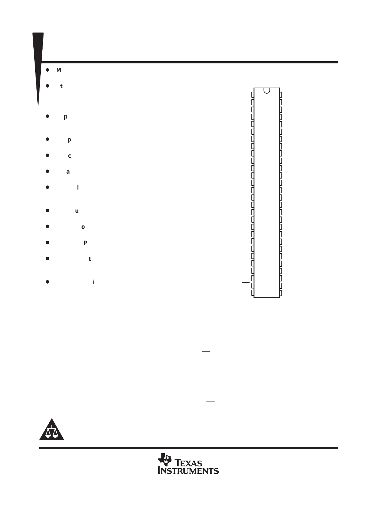
SN54LVTH16835. . . WD PACKAGE
SN74LVTH16835... DGG OR DL PACKAGE
(TOP VIEW)
1
2
3
4
5
6
7
8
9
10
11
12
13
14
15
16
17
18
19
20
21
22
23
24
25
26
27
28
56
55
54
53
52
51
50
49
48
47
46
45
44
43
42
41
40
39
38
37
36
35
34
33
32
31
30
29
NC
NC
Y1
GND
Y2
Y3
V
CC
Y4
Y5
Y6
GND
Y7
Y8
Y9
Y10
Y1 1
Y12
GND
Y13
Y14
Y15
V
CC
Y16
Y17
GND
Y18
OE
LE
GND
NC
A1
GND
A2
A3
V
CC
A4
A5
A6
GND
A7
A8
A9
A10
A1 1
A12
GND
A13
A14
A15
V
CC
A16
A17
GND
A18
CLK
GND
NC – No internal connection
Please be aware that an important notice concerning availability, standard warranty, and use in critical applications of
Texas Instruments semiconductor products and disclaimers thereto appears at the end of this data sheet.
SN54LVTH16835, SN74LVTH16835
3.3-V ABT 18-BIT UNIVERSAL BUS DRIVERS
WITH 3-STATE OUTPUTS
SCBS713C – MARCH 1998 – REVISED APRIL 1999
2
POST OFFICE BOX 655303 • DALLAS, TEXAS 75265
description (continued)
These devices are fully specified for hot-insertion applications using I
off
and power-up 3-state. The I
off
circuitry
disables the outputs, preventing damaging current backflow through the devices when they are powered down.
The power-up 3-state circuitry places the outputs in the high-impedance state during power up and power down,
which prevents driver conflict.
The SN54L VTH16835 is characterized for operation over the full military temperature range of –55°C to 125°C.
The SN74LVTH16835 is characterized for operation from –40°C to 85°C.
FUNCTION TABLE
INPUTS
OUTPUT
OE LE CLK A
Y
H X X X Z
L HXL L
LHXH H
LL↑LL
LL↑HH
LLHX Y
0
†
LLLX Y
0
‡
†
Output level before the indicated steady-state
input conditions were established, provided
that CLK is high before LE goes low
‡
Output level before the indicated steady-state
input conditions were established
SN54LVTH16835, SN74LVTH16835
3.3-V ABT 18-BIT UNIVERSAL BUS DRIVERS
WITH 3-STATE OUTPUTS
SCBS713C – MARCH 1998 – REVISED APRIL 1999
3
POST OFFICE BOX 655303 • DALLAS, TEXAS 75265
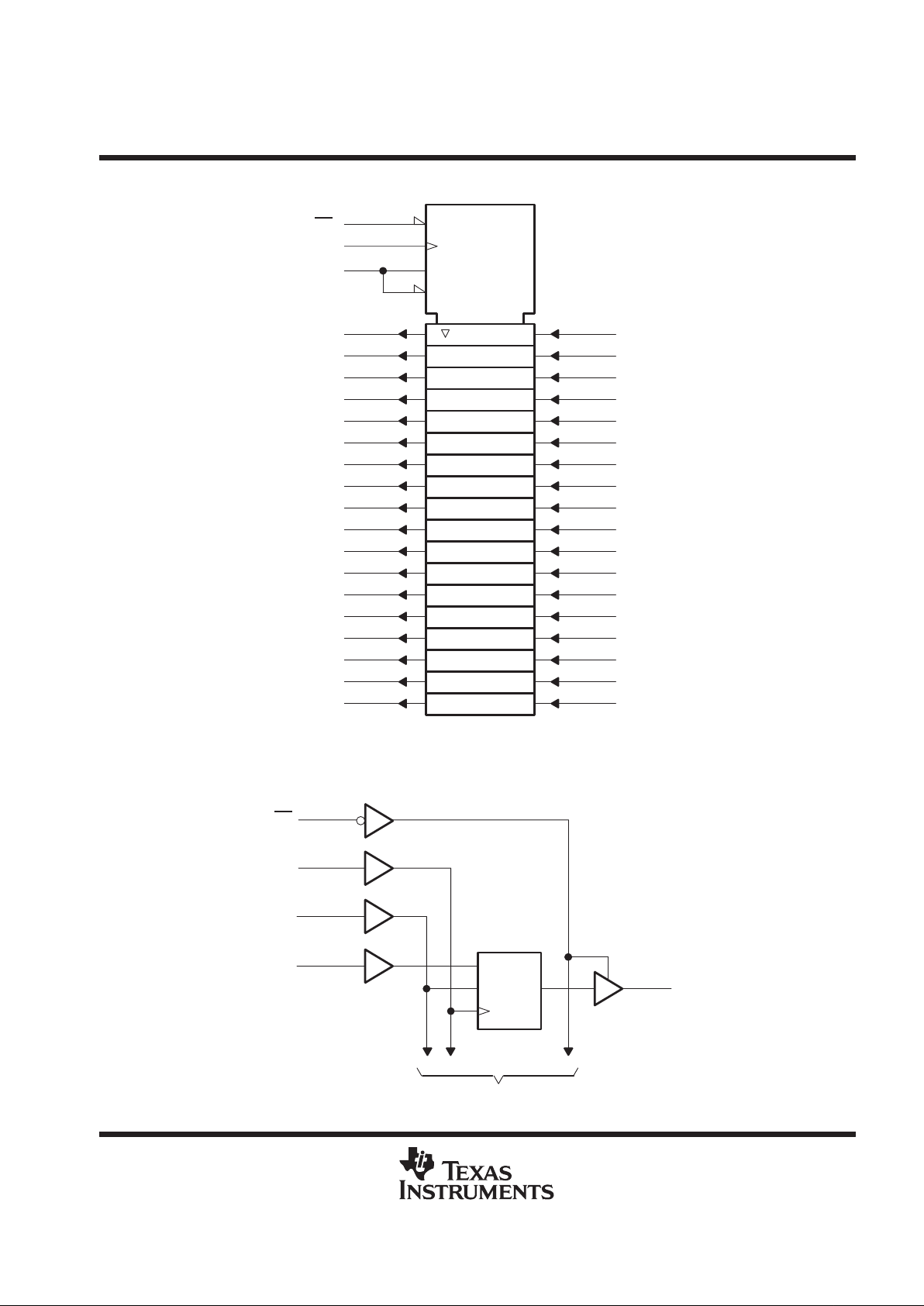
logic symbol
†
A6
47
A7
45
A8
44
A9
43
A10
42
A11
41
A12
40
A13
38
A14
37
A15
36
A16
34
A17
33
A18
31
OE
EN1
27
30
CLK
5
Y2
6
Y3
9
Y5
10
Y6
12
Y7
13
Y8
14
Y9
15
Y10
16
Y11
17
Y12
19
Y13
20
Y14
21
Y15
23
Y16
24
Y17
26
Y18
C3
28
LE
G2
†
This symbol is in accordance with ANSI/IEEE Std 91-1984 and IEC Publication 617-12.
2C3
8
Y4
1
1
3
Y1 A1
54
3D
A2
52
A3
51
A4
49
A5
48
logic diagram (positive logic)
OE
CLK
Y1
1D
C1
CLK
To 17 Other Channels
LE
A1
27
30
28
54
3
 Loading...