

Page 1
查询SN54LVT245供应商
SN54LVT245B, SN74LVT245B
3.3-V ABT OCTAL BUS TRANSCEIVERS
WITH 3-STATE OUTPUTS
SCES004D – JANUARY 1995 – REVISED APRIL 2000
D
State-of-the-Art Advanced BiCMOS
Technology (ABT) Design for 3.3-V
Operation and Low Static-Power
Dissipation
D
Support Mixed-Mode Signal Operation (5-V
Input and Output Voltages With 3.3-V V
D
Support Unregulated Battery Operation
Down to 2.7 V
D
Typical V
(Output Ground Bounce)
OLP
<0.8 V at VCC = 3.3 V, TA = 25°C
D
I
and Power-Up 3-State Support Hot
off
Insertion
D
Latch-Up Performance Exceeds 100 mA Per
JESD 78, Class II
D
ESD Protection Exceeds JESD 22
– 2000-V Human-Body Model (A114-A)
– 200-V Machine Model (A115-A)
– 1000-V Charged-Device Model (C101)
D
Package Options Include Plastic
Small-Outline (DW), Shrink Small-Outline
(DB), and Thin Shrink Small-Outline (PW)
Packages, Ceramic Chip Carriers (FK),
Ceramic Flat (W) Packages, and Ceramic
(J) DIPs
CC
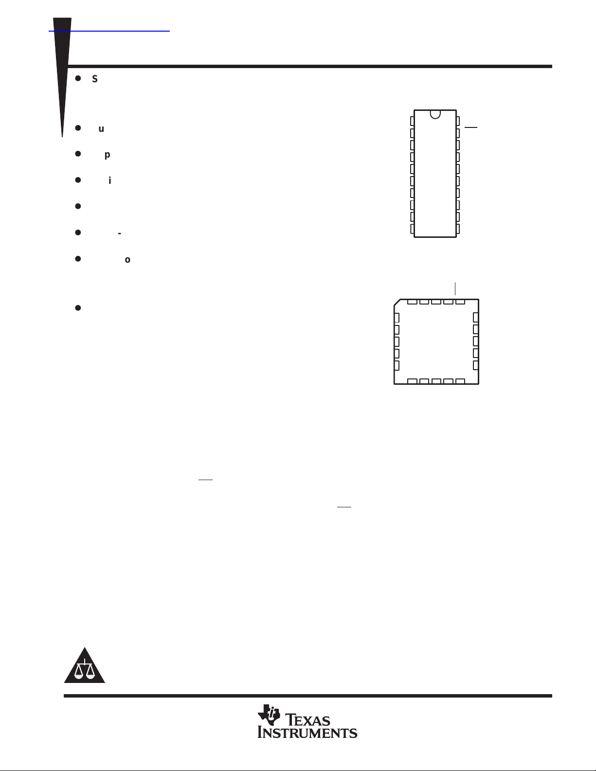
SN54LVT245B...J OR W PACKAGE
SN74LVT245B. .. DB, DW, OR PW PACKAGE
)
SN54LVT245B. . . FK PACKAGE
A3
A4
A5
A6
A7
(TOP VIEW)
1
DIR
2
A1
3
A2
4
A3
5
A4
6
A5
7
A6
8
A7
9
A8
GND
10
(TOP VIEW)
A2A1DIR
3212019
4
5
6
7
8
910111213
20
19
18
17
16
15
14
13
12
V
CC
OE
B1
B2
B3
B4
B5
B6
B7
11
B8
CC
OE
V
B1
18
B2
17
16
B3
15
B4
14
B5
description
These octal bus transceivers are designed
specifically for low-voltage (3.3-V) V
CC
A8
operation,
GND
B8
B7
B6
but with the capability to provide a TTL interface
to a 5-V system environment.
These devices are designed for asynchronous communication between data buses. They transmit data from
the A bus to the B bus or from the B bus to the A bus, depending on the logic level at the direction-control (DIR)
input. The output-enable (OE) input can be used to disable the devices so the buses are effectively isolated.
When VCC is between 0 and 1.5 V , the device is in the high-impedance state during power up or power down.
However, to ensure the high-impedance state above 1.5 V, OE should be tied to VCC through a pullup resistor;
the minimum value of the resistor is determined by the current-sinking capability of the driver.
These devices are fully specified for hot-insertion applications using I
and power-up 3-state. The I
off
disables the outputs, preventing damaging current backflow through the devices when they are powered down.
The power-up 3-state circuitry places the outputs in the high-impedance state during power up and power down,
which prevents driver conflict.
The SN54LVT245B is characterized for operation over the full military temperature range of –55°C to 125°C.
The SN74LVT245B is characterized for operation from –40°C to 85°C.
Please be aware that an important notice concerning availability, standard warranty, and use in critical applications of
Texas Instruments semiconductor products and disclaimers thereto appears at the end of this data sheet.
circuitry
off
UNLESS OTHERWISE NOTED this document contains PRODUCTION
DATA information current as of publication date. Products conform to
specifications per the terms of Texas Instruments standard warranty.
Production processing does not necessarily include testing of all
parameters.
POST OFFICE BOX 655303 • DALLAS, TEXAS 75265
Copyright 2000, Texas Instruments Incorporated
1
Page 2
SN54LVT245B, SN74LVT245B
OPERATION
3.3-V ABT OCTAL BUS TRANSCEIVERS
WITH 3-STATE OUTPUTS
SCES004D – JANUARY 1995 – REVISED APRIL 2000
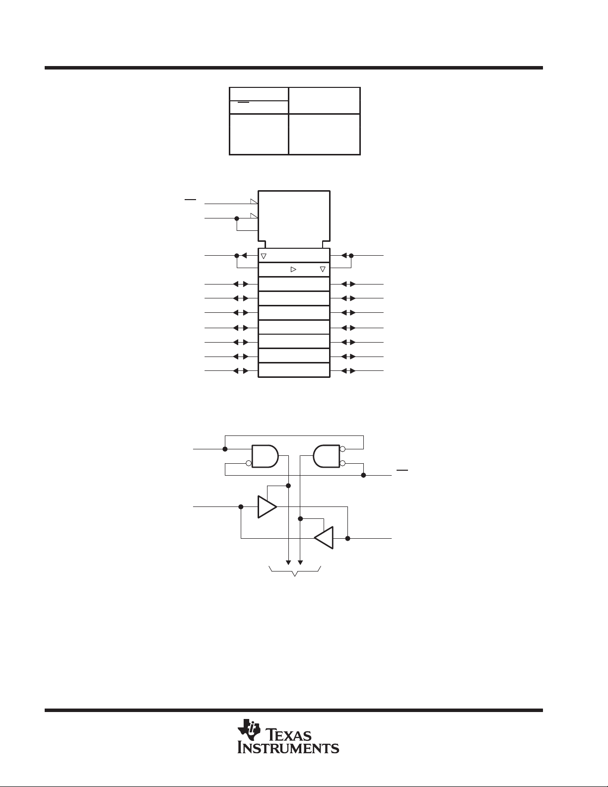
INPUTS
OE DIR
L L B data to A bus
L H A data to B bus
H X Isolation
FUNCTION TABLE
logic symbol
†
This symbol is in accordance with ANSI/IEEE Std 91-1984 and IEC Publication 617-12.
†
OE
DIR
A1
A2
A3
A4
A5
A6
A7
A8
19
1
2
3
4
5
6
7
8
9
G3
3EN1[BA]
3EN2[AB]
1
2
logic diagram (positive logic)
1
DIR
18
17
16
15
14
13
12
11
B1
B2
B3
B4
B5
B6
B7
B8
A1
19
OE
2
18
B1
To Seven Other Channels
2
POST OFFICE BOX 655303 • DALLAS, TEXAS 75265
Page 3
UNIT
SN54LVT245B, SN74LVT245B
3.3-V ABT OCTAL BUS TRANSCEIVERS
WITH 3-STATE OUTPUTS
SCES004D – JANUARY 1995 – REVISED APRIL 2000
absolute maximum ratings over operating free-air temperature range (unless otherwise noted)
†
Supply voltage range, VCC –0.5 V to 4.6 V. . . . . . . . . . . . . . . . . . . . . . . . . . . . . . . . . . . . . . . . . . . . . . . . . . . . . . . . .
Input voltage range, VI (see Note 1) –0.5 V to 7 V. . . . . . . . . . . . . . . . . . . . . . . . . . . . . . . . . . . . . . . . . . . . . . . . . .
Voltage range applied to any output in the high-impedance
or power-off state, V
Voltage range applied to any output in the high state, V
(see Note 1) –0.5 V to 7 V. . . . . . . . . . . . . . . . . . . . . . . . . . . . . . . . . . . . . . . . . . . . . . . .
O
(see Note 1) –0.5 V to V
O
CC
+ 0.5 V. . . . . . . . . . . . .
Current into any output in the low state, IO: SN54LVT245B 96 mA. . . . . . . . . . . . . . . . . . . . . . . . . . . . . . . . . . .
SN74LVT245B 128 mA. . . . . . . . . . . . . . . . . . . . . . . . . . . . . . . . . . .
Current into any output in the high state, I
(see Note 2): SN54LVT245B 48 mA. . . . . . . . . . . . . . . . . . . . . . . .
O
SN74LVT245B 64 mA. . . . . . . . . . . . . . . . . . . . . . . .
Input clamp current, I
Output clamp current, I
Package thermal impedance, θ
(V
< 0) –50 mA. . . . . . . . . . . . . . . . . . . . . . . . . . . . . . . . . . . . . . . . . . . . . . . . . . . . . . . . . . .
IK
I
(V
< 0) –50 mA. . . . . . . . . . . . . . . . . . . . . . . . . . . . . . . . . . . . . . . . . . . . . . . . . . . . . . . .
OK
O
(see Note 3): DB package 70°C/W. . . . . . . . . . . . . . . . . . . . . . . . . . . . . . . . .
JA
DW package 58°C/W. . . . . . . . . . . . . . . . . . . . . . . . . . . . . . . . .
PW package 83°C/W. . . . . . . . . . . . . . . . . . . . . . . . . . . . . . . . .
Storage temperature range, T
†
Stresses beyond those listed under “absolute maximum ratings” may cause permanent damage to the device. These are stress ratings only, and
functional operation of the device at these or any other conditions beyond those indicated under “recommended operating conditions” is not
implied. Exposure to absolute-maximum-rated conditions for extended periods may affect device reliability.
NOTES: 1. The input and output negative-voltage ratings may be exceeded if the input and output clamp-current ratings are observed.
2. This current flows only when the output is in the high state and VO > VCC.
3. The package thermal impedance is calculated in accordance with JESD 51.
–65°C to 150°C. . . . . . . . . . . . . . . . . . . . . . . . . . . . . . . . . . . . . . . . . . . . . . . . . . .
stg
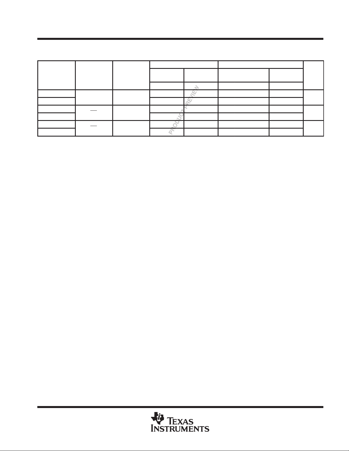
recommended operating conditions (see Note 4)
SN54LVT245B SN74LVT245B
MIN MAX MIN MAX
V
CC
V
IH
V
IL
V
I
I
OH
I
OL
∆t/∆v Input transition rise or fall rate Outputs enabled 10 10 ns/V
∆t/∆V
T
A
NOTE 4: All unused inputs of the device must be held at VCC or GND to ensure proper device operation. Refer to the TI application report,
Supply voltage 2.7 3.6 2.7 3.6 V
High-level input voltage 2 2 V
Low-level input voltage 0.8 0.8 V
Input voltage 5.5 5.5 V
High-level output current –24 –32 mA
Low-level output current 48 64 mA
Power-up ramp rate 200 200 µs/V
CC
Operating free-air temperature –55 125 –40 85 °C
Implications of Slow or Floating CMOS Inputs
, literature number SCBA004.
PRODUCT PREVIEW information concerns products in the formative or
design phase of development. Characteristic data and other
specifications are design goals. Texas Instruments reserves the right to
change or discontinue these products without notice.
POST OFFICE BOX 655303 • DALLAS, TEXAS 75265
3
Page 4
SN54LVT245B, SN74LVT245B
PARAMETER
TEST CONDITIONS
UNIT
V
V
V
V
V
2.7 V
V
V
V
V
Control inputs
‡
V
CC
3.3-V ABT OCTAL BUS TRANSCEIVERS
WITH 3-STATE OUTPUTS
SCES004D – JANUARY 1995 – REVISED APRIL 2000
electrical characteristics over recommended operating free-air temperature range (unless
otherwise noted)
SN54LVT245B SN74LVT245B
MIN TYP†MAX MIN TYP†MAX
V
IK
OH
OL
I
I
A or B ports
I
off
I
OZH
I
OZL
I
OZPU
I
OZPD
I
CC
§
∆I
CC
C
i
C
io
∗
On products compliant to MIL-PRF-38535, this parameter is not production tested.
†
All typical values are at VCC = 3.3 V, TA = 25°C.
‡
Unused terminals are at VCC or GND.
§
This is the increase in supply current for each input that is at the specified TTL-voltage level rather than VCC or GND.
VCC = 2.7 V, II = –18 mA –1.2 –1.2 V
VCC = 2.7 V to 3.6 V, IOH = –100 µA VCC–0.2 VCC–0.2
VCC = 2.7 V, IOH = –8 mA 2.4 2.4
= 3
CC
=
CC
= 3
CC
VCC = 3.6 V, VI = VCC or GND ±1 ±1
p
VCC = 0 or 3.6 V, VI = 5.5 V 10 10
VCC = 3.6 V
VCC = 0, VI or VO = 0 to 4.5 V ±100 µA
VCC = 3.6 V, VO = 3 V 5 5 µA
VCC = 3.6 V, VO = 0.5 V –5 –5 µA
VCC = 0 to 1.5 V, VO = 0.5 V to 3 V,
OE
= don’t care
VCC = 1.5 V to 0, VO = 0.5 V to 3 V,
OE
= don’t care
=
= 3.6 V,
IO = 0,
VI = VCC or GND
VCC = 3 V to 3.6 V, One input at VCC – 0.6 V,
Other inputs at VCC or GND
VI = 3 V or 0 4 4 pF
VO = 3 V or 0 9 9 pF
IOH = –24 mA 2
IOH = –32 mA 2
IOL = 100 µA 0.2 0.2
IOL = 24 mA 0.5 0.5
IOL = 16 mA 0.4 0.4
IOL = 32 mA 0.5 0.5
IOL = 48 mA 0.55
IOL = 64 mA 0.55
VI = 5.5 V 20 20
VI = V
CC
VI = 0 –5 –5
Outputs high 0.19 0.19
Outputs low 5 5
Outputs disabled 0.19 0.19
1 1
∗
±100
∗
±100
0.2 0.2 mA
µA
±100 µA
±100 µA
mA
PRODUCT PREVIEW information concerns products in the formative or
design phase of development. Characteristic data and other
specifications are design goals. Texas Instruments reserves the right to
change or discontinue these products without notice.
4
POST OFFICE BOX 655303 • DALLAS, TEXAS 75265
Page 5
A or B
B or A
ns
OE
A or B
ns
OE
A or B
ns
SN54LVT245B, SN74LVT245B
3.3-V ABT OCTAL BUS TRANSCEIVERS
WITH 3-STATE OUTPUTS
SCES004D – JANUARY 1995 – REVISED APRIL 2000
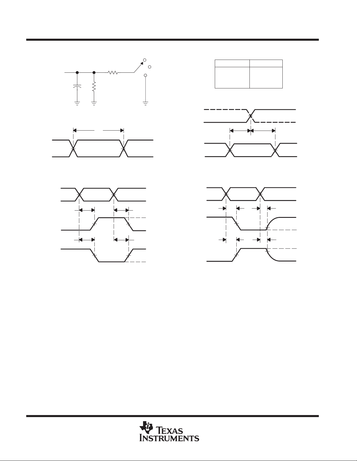
switching characteristics over recommended operating free-air temperature range, CL = 50 pF
(unless otherwise noted) (see Figure 1)
SN54LVT245B SN74LVT245B
PARAMETER
t
PLH
t
PHL
t
PZH
t
PZL
t
PHZ
t
PLZ
†
All typical values are at VCC = 3.3 V, TA = 25°C.
FROM
(INPUT)
TO
(OUTPUT)
VCC = 3.3 V
± 0.3 V
MIN MAX MIN MAX MIN TYP†MAX MIN MAX
1.1 3.7 4.2 1.2 2.3 3.5 4
1.1 3.7 4.2 1.2 2.1 3.5 4
1.2 5.7 7.4 1.3 3.2 5.5 7.1
1.6 5.7 6.8 1.7 3.4 5.5 6.5
2.1 6.2 6.8 2.2 3.5 5.9 6.5
2.1 5.3 5.5 2.2 3.4 5 5.1
VCC = 2.7 V
VCC = 3.3 V
± 0.3 V
VCC = 2.7 V
UNIT
PRODUCT PREVIEW information concerns products in the formative or
design phase of development. Characteristic data and other
specifications are design goals. Texas Instruments reserves the right to
change or discontinue these products without notice.
POST OFFICE BOX 655303 • DALLAS, TEXAS 75265
5
Page 6
SN54LVT245B, SN74LVT245B
3.3-V ABT OCTAL BUS TRANSCEIVERS
WITH 3-STATE OUTPUTS
SCES004D – JANUARY 1995 – REVISED APRIL 2000
PARAMETER MEASUREMENT INFORMATION
S1
1.5 V
1.5 V
1.5 V1.5 V
500 Ω
t
w
1.5 V
500 Ω
From Output
Under Test
CL = 50 pF
(see Note A)
LOAD CIRCUIT
Input
Input
Output
Output
INVERTING AND NONINVERTING OUTPUTS
NOTES: A. CL includes probe and jig capacitance.
B. Waveform 1 is for an output with internal conditions such that the output is low except when disabled by the output control.
Waveform 2 is for an output with internal conditions such that the output is high except when disabled by the output control.
C. All input pulses are supplied by generators having the following characteristics: PRR ≤ 10 MHz, ZO = 50 Ω, tr ≤ 2.5 ns, tf≤ 2.5 ns.
D. The outputs are measured one at a time with one transition per measurement.
1.5 V
VOLTAGE WAVEFORMS
PULSE DURATION
1.5 V 1.5 V
t
PLH
t
PHL
VOLTAGE WAVEFORMS
PROPAGATION DELAY TIMES
t
PHL
t
PLH
6 V
GND
2.7 V
0 V
V
OH
V
OL
V
OH
V
OL
Open
2.7 V
0 V
Timing Input
Data Input
Output
Control
Output
Waveform 1
S1 at 6 V
(see Note B)
Output
Waveform 2
S1 at GND
(see Note B)
TEST S1
t
PLH/tPHL
t
PLZ/tPZL
t
PHZ/tPZH
t
su
1.5 V 1.5 V
VOLTAGE WAVEFORMS
SETUP AND HOLD TIMES
t
PZL
1.5 V
t
PZH
1.5 V
VOLTAGE WAVEFORMS
ENABLE AND DISABLE TIMES
LOW- AND HIGH-LEVEL ENABLING
Open
GND
1.5 V
t
6 V
h
1.5 V1.5 V
VOL + 0.3 V
VOH – 0.3 V
t
PLZ
t
PHZ
2.7 V
0 V
2.7 V
0 V
2.7 V
0 V
3 V
V
OL
V
OH
≈ 0 V
Figure 1. Load Circuit and Voltage Waveforms
6
POST OFFICE BOX 655303 • DALLAS, TEXAS 75265
Page 7

IMPORTANT NOTICE
T exas Instruments and its subsidiaries (TI) reserve the right to make changes to their products or to discontinue
any product or service without notice, and advise customers to obtain the latest version of relevant information
to verify, before placing orders, that information being relied on is current and complete. All products are sold
subject to the terms and conditions of sale supplied at the time of order acknowledgment, including those
pertaining to warranty, patent infringement, and limitation of liability.
TI warrants performance of its semiconductor products to the specifications applicable at the time of sale in
accordance with TI’s standard warranty. Testing and other quality control techniques are utilized to the extent
TI deems necessary to support this warranty . Specific testing of all parameters of each device is not necessarily
performed, except those mandated by government requirements.
Customers are responsible for their applications using TI components.
In order to minimize risks associated with the customer’s applications, adequate design and operating
safeguards must be provided by the customer to minimize inherent or procedural hazards.
TI assumes no liability for applications assistance or customer product design. TI does not warrant or represent
that any license, either express or implied, is granted under any patent right, copyright, mask work right, or other
intellectual property right of TI covering or relating to any combination, machine, or process in which such
semiconductor products or services might be or are used. TI’s publication of information regarding any third
party’s products or services does not constitute TI’s approval, warranty or endorsement thereof.
Copyright 2000, Texas Instruments Incorporated
 Loading...