Texas Instruments SN74LVCZ240ADBR, SN74LVCZ240ADGVR, SN74LVCZ240ADW, SN74LVCZ240ADWR, SN74LVCZ240AN Datasheet
...
SN74LVCZ240A
OCTAL BUFFER/DRIVER
WITH 3-STATE OUTPUTS
SCES273B – JUNE 1999 – REVISED JANUARY 2000
1
POST OFFICE BOX 655303 • DALLAS, TEXAS 75265
D
EPIC
(Enhanced-Performance Implanted
CMOS) Submicron Process
D
T ypical V
OLP
(Output Ground Bounce)
<0.8 V at VCC = 3.3 V, TA = 25°C
D
T ypical V
OHV
(Output VOH Undershoot)
>2 V at V
CC
= 3.3 V, TA = 25°C
D
I
off
and Power-Up 3-State Support Hot
Insertion
D
Supports Mixed-Mode Signal Operation on
All Ports (5-V Input/Output Voltage With
3.3-V VCC)
D
Latch-Up Performance Exceeds 100 mA Per
JESD 78, Class II
D
Package Options Include Shrink
Small-Outline (DB), Plastic Thin Very
Small-Outline (DGV), Small-Outline (DW),
and Thin Shrink Small-Outline (PW)
Packages
description
This octal buffer/driver is designed for 2.7-V to 3.6-V VCC operation.
The SN74LVCZ240A is designed specifically to improve the performance and density of 3-state memory
address drivers, clock drivers, and bus-oriented receivers and transmitters.
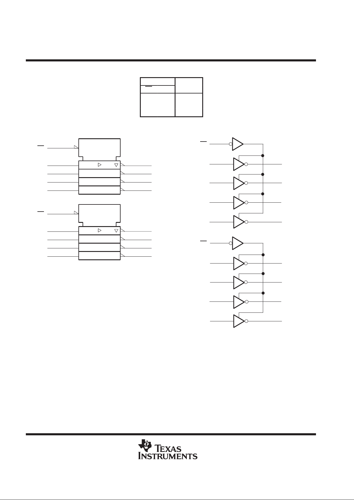
This device is organized as two 4-bit buffers/drivers with separate output-enable (OE) inputs. When OE is low ,
the device passes data from the A inputs to the Y outputs. When OE is high, the outputs are in the
high-impedance state.
Inputs can be driven from either 3.3-V or 5-V devices. This feature allows the use of these devices as translators
in a mixed 3.3-V/5-V system environment.
When VCC is between 0 and 1.5 V , the device is in the high-impedance state during power up or power down.
However, to ensure the high-impedance state above 1.5 V, OE should be tied to VCC through a pullup resistor;
the minimum value of the resistor is determined by the current-sinking capability of the driver.
This device is fully specified for hot-insertion applications using I
off
and power-up 3-state. The I
off
circuitry
disables the outputs, preventing damaging current backflow through the device when it is powered down. The
power-up 3-state circuitry places the outputs in the high-impedance state during power up and power down,
which prevents driver conflict.
The SN74LVCZ240A is characterized for operation from –40°C to 85°C.
Copyright 2000, Texas Instruments Incorporated
PRODUCTION DATA information is current as of publication date.
Products conform to specifications per the terms of Texas Instruments
standard warranty. Production processing does not necessarily include
testing of all parameters.
Please be aware that an important notice concerning availability, standard warranty, and use in critical applications of
Texas Instruments semiconductor products and disclaimers thereto appears at the end of this data sheet.
EPIC is a trademark of Texas Instruments Incorporated.
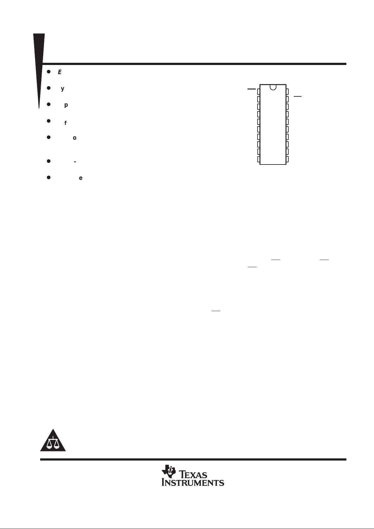
DB, DGV, DW, OR PW PACKAGE
(TOP VIEW)
1
2
3
4
5
6
7
8
9
10
20
19
18
17
16
15
14
13
12
11
1OE
1A1
2Y4
1A2
2Y3
1A3
2Y2
1A4
2Y1
GND
V
CC
2OE
1Y1
2A4
1Y2
2A3
1Y3
2A2
1Y4
2A1

SN74LVCZ240A
OCTAL BUFFER/DRIVER
WITH 3-STATE OUTPUTS
SCES273B – JUNE 1999 – REVISED JANUARY 2000
2
POST OFFICE BOX 655303 • DALLAS, TEXAS 75265
FUNCTION TABLE
(each buffer)
INPUTS
OUTPUT
OE A
Y
L H L
L LH
H X Z
logic symbol
†
†
This symbol is in accordance with ANSI/IEEE Std 91-1984 and
IEC Publication 617-12.
2
1A1
4
1A2
6
1A3
8
1A4
EN
1
1Y1
18
1Y2
16
1Y3
14
1Y4
12
11
2A1
13
2A2
15
2A3
17
2A4
EN
19
2Y1
9
2Y2
7
2Y3
5
2Y4
3
1OE
2OE
logic diagram (positive logic)
1
2
4
6
8
19
11
13
15
17 3
5
7
9
12
14
16
18
1A1
1A2
1A3
1A4
1Y1
2A1
2A2
2A3
2A4
2Y1
1Y2
1Y3
1Y4
2Y2
2Y3
2Y4
1OE
2OE
 Loading...