

Texas Instruments SN74LVCHR162245ADGGR, SN74LVCHR162245ADL, SN74LVCHR162245ADLR, SN74LVCHR16245AGR, SN74LVCHR16245ALR Datasheet
SN74LVCHR16245A
16-BIT BUS TRANSCEIVER
WITH 3-STATE OUTPUTS
SCAS582G – NOVEMBER 1996 – REVISED JUNE 1999
1
POST OFFICE BOX 655303 • DALLAS, TEXAS 75265
D
Member of the Texas Instruments
Widebus
Family
D
EPIC
(Enhanced-Performance Implanted
CMOS) Submicron Process
D
T ypical V
OLP
(Output Ground Bounce)
< 0.8 V at V
CC
= 3.3 V, TA = 25°C
D
T ypical V
OHV
(Output VOH Undershoot)
> 2 V at V
CC
= 3.3 V, TA = 25°C
D
Supports Mixed-Mode Signal Operation on
All Ports (5-V Input/Output Voltage With
3.3-V V
CC
)
D
Power Off Disables Inputs/Outputs,
Permitting Live Insertion
D
ESD Protection Exceeds 2000 V Per
MIL-STD-883, Method 3015; Exceeds 200 V
Using Machine Model (C = 200 pF, R = 0)
D
Latch-Up Performance Exceeds 250 mA Per
JESD 17
D
Bus Hold on Data Inputs Eliminates the
Need for External Pullup/Pulldown
Resistors
D
All Outputs Have Equivalent 26-Ω Series
Resistors, So No External Resistors Are
Required
D
Package Options Include Plastic 300-mil
Shrink Small-Outline (DL) and Thin Shrink
Small-Outline (DGG) Packages
NOTE: For order entry:
The DGG package is abbreviated to G.
For tape and reel:
The DGGR package is abbreviated to GR, and
the DLR package is abbreviated to LR.
description
This 16-bit (dual-octal) noninverting bus transceiver is designed for 1.65-V to 3.6-V VCC operation.
The SN74LVCHR16245A is designed for asynchronous communication between data buses. The
control-function implementation minimizes external-timing requirements.
This device can be used as two 8-bit transceivers or one 16-bit transceiver. It allows data transmission from the
A bus to the B bus or from the B bus to the A bus, depending on the logic level at the direction-control (DIR)
input. The output-enable (OE
) input can disable the device so that the buses are effectively isolated.
All outputs, which are designed to sink up to 12 mA, include equivalent 26-W series resistors to reduce
overshoot and undershoot.
T o ensure the high-impedance state during power up or power down, OE
should be tied to VCC through a pullup
resistor; the minimum value of the resistor is determined by the current-sinking capability of the driver.
PRODUCTION DATA information is current as of publication date.
Products conform to specifications per the terms of Texas Instruments
standard warranty. Production processing does not necessarily include
testing of all parameters.
Copyright 1999, Texas Instruments Incorporated
Please be aware that an important notice concerning availability, standard warranty, and use in critical applications of
Texas Instruments semiconductor products and disclaimers thereto appears at the end of this data sheet.
EPIC and Widebus are trademarks of Texas Instruments Incorporated.
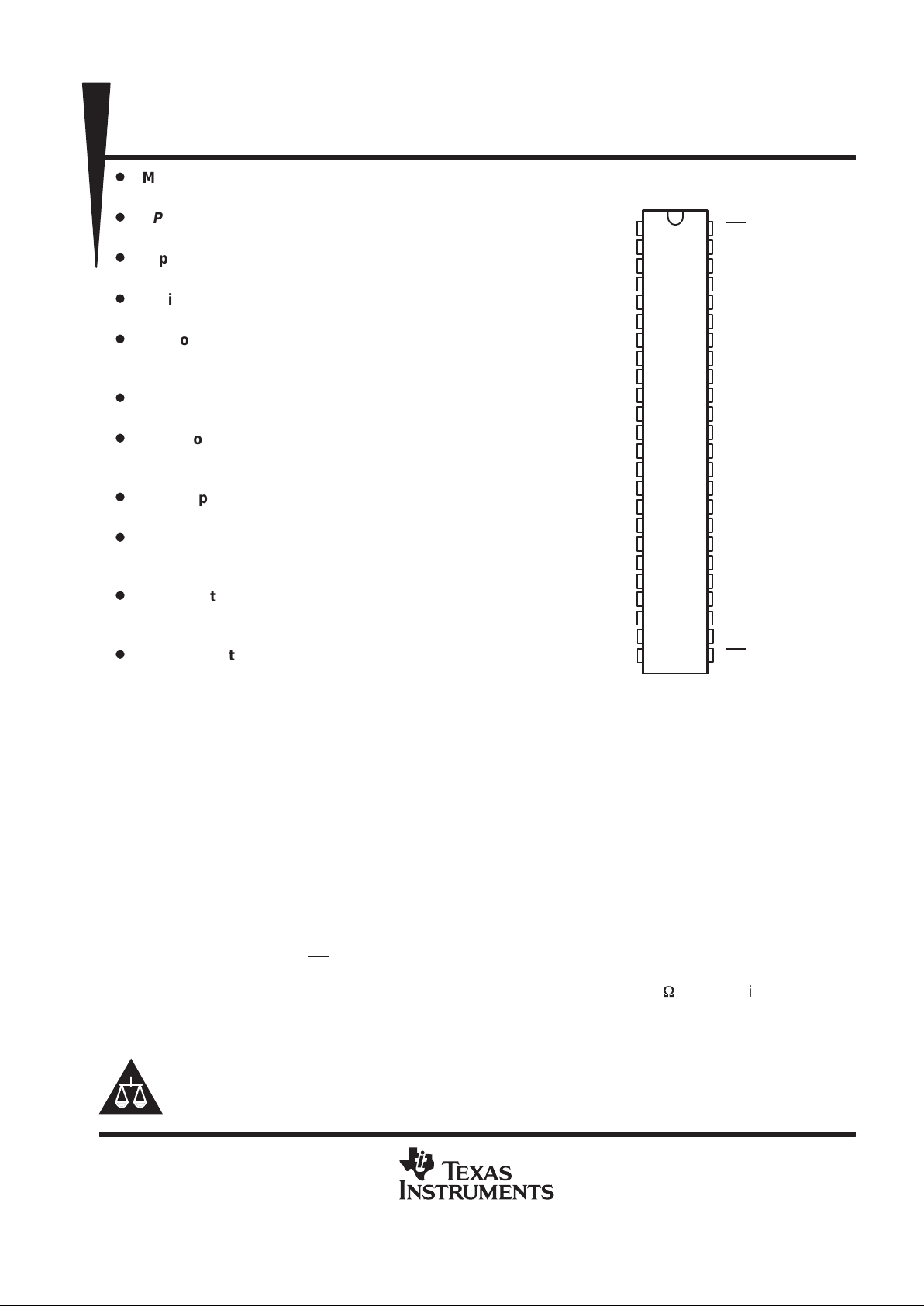
DGG OR DL PACKAGE
(TOP VIEW)
1
2
3
4
5
6
7
8
9
10
11
12
13
14
15
16
17
18
19
20
21
22
23
24
48
47
46
45
44
43
42
41
40
39
38
37
36
35
34
33
32
31
30
29
28
27
26
25
1DIR
1B1
1B2
GND
1B3
1B4
V
CC
1B5
1B6
GND
1B7
1B8
2B1
2B2
GND
2B3
2B4
V
CC
2B5
2B6
GND
2B7
2B8
2DIR
1OE
1A1
1A2
GND
1A3
1A4
V
CC
1A5
1A6
GND
1A7
1A8
2A1
2A2
GND
2A3
2A4
V
CC
2A5
2A6
GND
2A7
2A8
2OE

SN74LVCHR16245A
16-BIT BUS TRANSCEIVER
WITH 3-STATE OUTPUTS
SCAS582G – NOVEMBER 1996 – REVISED JUNE 1999
2
POST OFFICE BOX 655303 • DALLAS, TEXAS 75265
description (continued)
Inputs can be driven from either 3.3-V or 5-V devices. This feature allows the use of these devices as translators
in a mixed 3.3-V/5-V system environment.
Active bus-hold circuitry is provided to hold unused or floating data inputs at a valid logic level.
The SN74LVCHR16245A is characterized for operation from –40°C to 85°C.
FUNCTION TABLE
(each 8-bit section)
INPUTS
OE DIR
OPERATION
L L B data to A bus
L H A data to B bus
H X Isolation
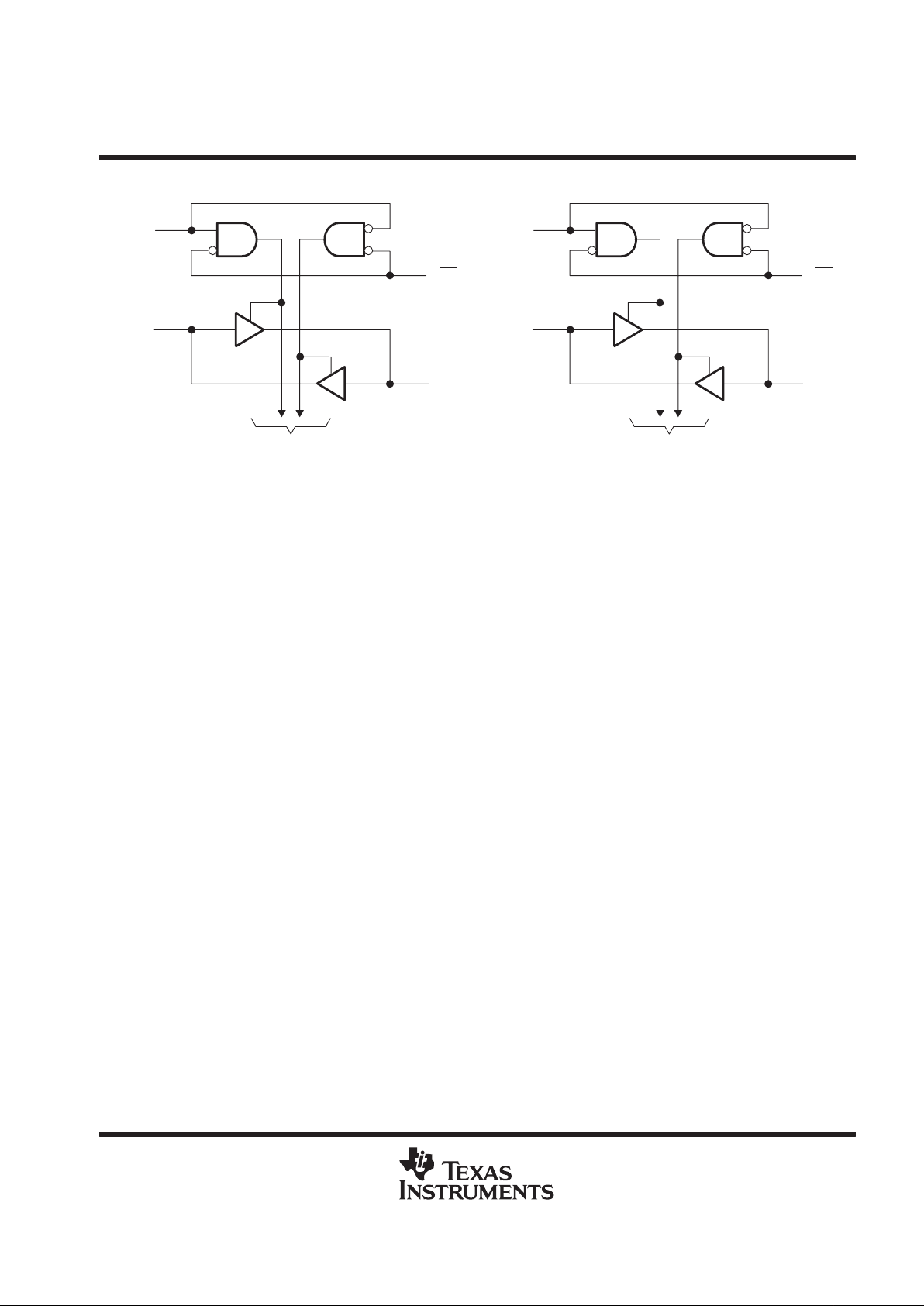
logic symbol
†
1A2
46
1A3
44
1A4
43
1A5
41
1A6
40
1A7
38
1A8
37
2A2
35
2A3
33
2A4
32
2A5
30
2A6
29
2A7
27
2A8
26
1OE
2OE
†
This symbol is in accordance with ANSI/IEEE Std 91-1984 and IEC Publication 617-12.
1A1
47
G3
48
3 EN1 [BA]
1
1DIR
3 EN2 [AB]
G6
25
6 EN4 [BA]
24
2DIR
6 EN5 [AB]
1B1
2
1B2
3
1B3
5
1B4
6
1B5
8
1B6
9
1B7
11
1B8
12
2A1
36
2B1
13
2B2
14
2B3
16
2B4
17
2B5
19
2B6
20
2B7
22
2B8
23
1
4
2
5
SN74LVCHR16245A
16-BIT BUS TRANSCEIVER
WITH 3-STATE OUTPUTS
SCAS582G – NOVEMBER 1996 – REVISED JUNE 1999
3
POST OFFICE BOX 655303 • DALLAS, TEXAS 75265
logic diagram (positive logic)
To Seven Other Channels
1DIR
1A1
1B1
1OE
To Seven Other Channels
2DIR
2A1
2B1
2OE
1
47
24
36
48
2
25
13
absolute maximum ratings over operating free-air temperature range (unless otherwise noted)
†
Supply voltage range, V
CC
–0.5 V to 6.5 V. . . . . . . . . . . . . . . . . . . . . . . . . . . . . . . . . . . . . . . . . . . . . . . . . . . . . . . . .
Input voltage range, V
I
(see Note 1) –0.5 V to 6.5 V. . . . . . . . . . . . . . . . . . . . . . . . . . . . . . . . . . . . . . . . . . . . . . . . .
Voltage range applied to any output in the high-impedance or power-off state, V
O
(see Note 1) –0.5 V to 6.5 V. . . . . . . . . . . . . . . . . . . . . . . . . . . . . . . . . . . . . . . . . . . . . . . . . . . . . . . . . . . . . . . . . . .
Voltage range applied to any output in the high or low state, V
O
(see Notes 1 and 2) –0.5 V to VCC + 0.5 V. . . . . . . . . . . . . . . . . . . . . . . . . . . . . . . . . . . . . . . . . . . . . . . . . . . . . . .
Input clamp current, I
IK
(VI < 0) –50 mA. . . . . . . . . . . . . . . . . . . . . . . . . . . . . . . . . . . . . . . . . . . . . . . . . . . . . . . . . . .
Output clamp current, I
OK
(VO < 0) –50 mA. . . . . . . . . . . . . . . . . . . . . . . . . . . . . . . . . . . . . . . . . . . . . . . . . . . . . . . .
Continuous output current, I
O
±50 mA. . . . . . . . . . . . . . . . . . . . . . . . . . . . . . . . . . . . . . . . . . . . . . . . . . . . . . . . . . . . .
Continuous current through each V
CC
or GND ±100 mA. . . . . . . . . . . . . . . . . . . . . . . . . . . . . . . . . . . . . . . . . . . . .
Package thermal impedance, θ
JA
(see Note 3): DGG package 89°C/W. . . . . . . . . . . . . . . . . . . . . . . . . . . . . . . .
DL package 97°C/W. . . . . . . . . . . . . . . . . . . . . . . . . . . . . . . . . .
Storage temperature range, T
stg
–65°C to 150°C. . . . . . . . . . . . . . . . . . . . . . . . . . . . . . . . . . . . . . . . . . . . . . . . . . .
†
Stresses beyond those listed under “absolute maximum ratings” may cause permanent damage to the device. These are stress ratings only, and
functional operation of the device at these or any other conditions beyond those indicated under “recommended operating conditions” is not
implied. Exposure to absolute-maximum-rated conditions for extended periods may affect device reliability.
NOTES: 1. The input negative-voltage and output voltage ratings may be exceeded if the input and output current ratings are observed.
2. The value of VCC is provided in the recommended operating conditions table.
3. The package thermal impedance is calculated in accordance with JESD 51.
 Loading...