

Datasheet SN74LVCC3245ADBLE, SN74LVCC3245ADBR, SN74LVCC3245ADW, SN74LVCC3245ADWR, SN74LVCC3245APWLE Datasheet (Texas Instruments)
...
OPERATION
SN74LVCC3245A
OCTAL BUS TRANSCEIVER WITH ADJUSTABLE OUTPUT VOLTAGE
AND 3-STATE OUTPUTS
SCAS585F – NOVEMBER 1996 – REVISED AUGUST 1998
D
EPIC
(Enhanced-Performance Implanted
CMOS) Submicron Process
D
ESD Protection Exceeds 2000 V Per
MIL-STD-883, Method 3015; Exceeds 200 V
Using Machine Model (C = 200 pF, R = 0)
D
Latch-Up Performance Exceeds 250 mA Per
JESD 17
D
Package Options Include Plastic
Small-Outline (DW), Shrink Small-Outline
(DB), and Thin Shrink Small-Outline (PW)
Packages
description
This 8-bit (octal) noninverting bus transceiver
contains two separate supply rails. The B port is
designed to track V
, which accepts voltages
CCB
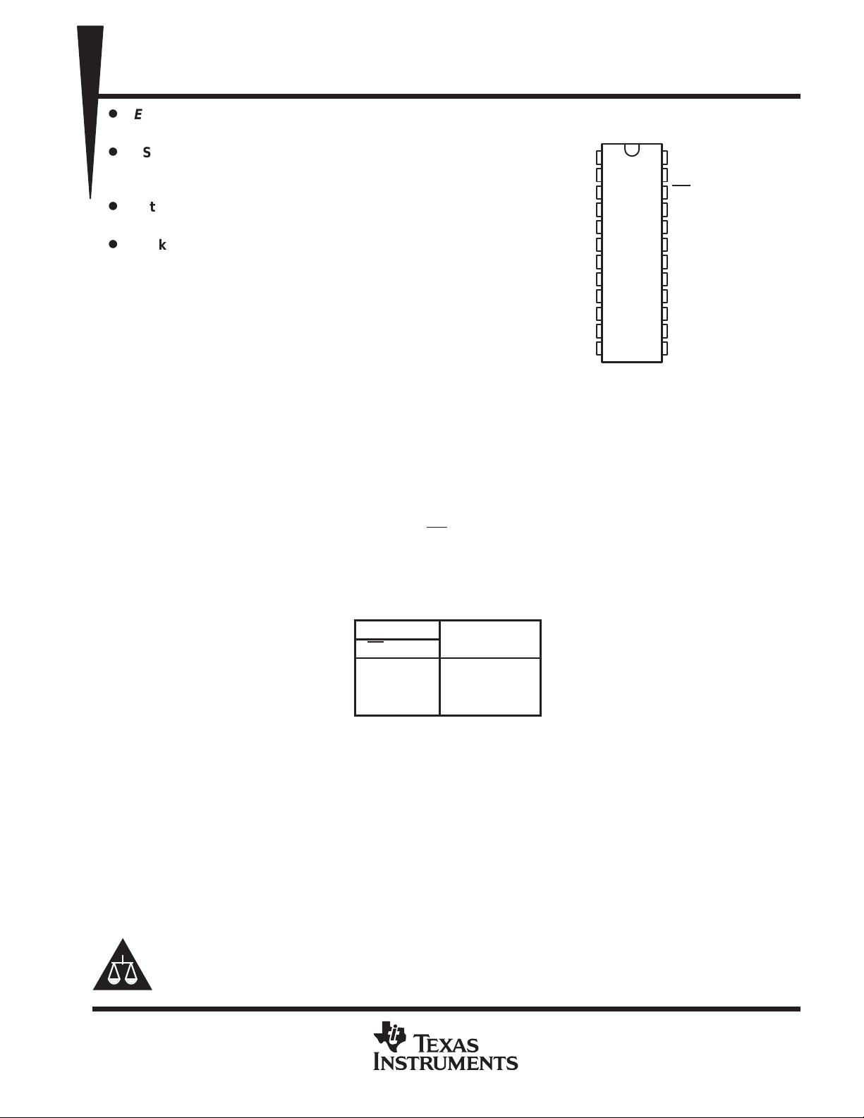
DB, DW, OR PW PACKAGE
(TOP VIEW)
V
GND
GND
NC – No internal connection
CCA
DIR
A1
A2
A3
A4
A5
A6
A7
A8
1
2
3
4
5
6
7
8
9
10
11
12
24
23
22
21
20
19
18
17
16
15
14
13
V
CCB
NC
OE
B1
B2
B3
B4
B5
B6
B7
B8
GND
from 3 V to 5.5 V, and the A port is designed to
track V
, which operates at 2.3 V to 3.6 V . This
CCA
allows for translation from a 3.3-V to a 5-V system
environment and vice versa, or from a 2.5-V to a
3.3-V system environment and vice versa.
The SN74LVCC3245A is designed for asynchronous communication between data buses. The device
transmits data from the A bus to the B bus or from the B bus to the A bus, depending on the logic level at the
direction-control (DIR) input. The output-enable (OE
) input can be used to disable the device so the buses are
effectively isolated.
The SN74LVCC3245A is characterized for operation from –40°C to 85°C.
FUNCTION TABLE
INPUTS
OE DIR
L L B data to A bus
L H A data to B bus
H X Isolation
Please be aware that an important notice concerning availability, standard warranty, and use in critical applications of
Texas Instruments semiconductor products and disclaimers thereto appears at the end of this data sheet.
EPIC is a trademark of Texas Instruments Incorporated.
PRODUCTION DATA information is current as of publication date.
Products conform to specifications per the terms of Texas Instruments
standard warranty. Production processing does not necessarily include
testing of all parameters.
POST OFFICE BOX 655303 • DALLAS, TEXAS 75265
Copyright 1998, Texas Instruments Incorporated
1
SN74LVCC3245A
OCTAL BUS TRANSCEIVER WITH ADJUSTABLE OUTPUT VOLTAGE
AND 3-STATE OUTPUTS
SCAS585F – NOVEMBER 1996 – REVISED AUGUST 1998
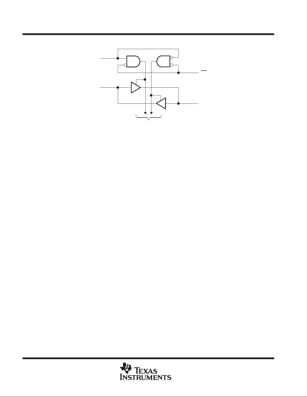
logic diagram (positive logic)
2
DIR
22
OE
3
A1
21
B1
To Seven Other Channels
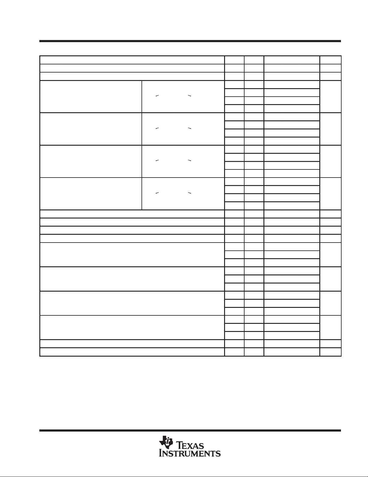
absolute maximum ratings over operating free-air temperature range (unless otherwise noted)
Supply voltage range, V
Input voltage range, V
and V
CCA
: All A port (see Note 2) –0.5 V to V
I
All B port (see Note 1) –0.5 V to V
Except I/O ports (see Note 2) –0.5 V to V
Output voltage range, V
Input clamp current, I
Output clamp current, I
Continuous output current, I
Continuous current through V
Package thermal impedance, θ
Storage temperature range, T
†
Stresses beyond those listed under “absolute maximum ratings” may cause permanent damage to the device. These are stress ratings only, and
functional operation of the device at these or any other conditions beyond those indicated under “recommended operating conditions” is not
implied. Exposure to absolute-maximum-rated conditions for extended periods may affect device reliability.
NOTES: 1. This value is limited to 6 V maximum.
2. This value is limited to 4.6 V maximum.
3. The package thermal impedance is calculated in accordance with JESD 51.
(see Note 1): All A port –0.5 V to V
O
(VI < 0) –50 mA. . . . . . . . . . . . . . . . . . . . . . . . . . . . . . . . . . . . . . . . . . . . . . . . . . . . . . . . . . .
IK
(VO < 0) –50 mA. . . . . . . . . . . . . . . . . . . . . . . . . . . . . . . . . . . . . . . . . . . . . . . . . . . . . . . .
OK
±50 mA. . . . . . . . . . . . . . . . . . . . . . . . . . . . . . . . . . . . . . . . . . . . . . . . . . . . . . . . . . . . .
O
CCA
JA
–65°C to 150°C. . . . . . . . . . . . . . . . . . . . . . . . . . . . . . . . . . . . . . . . . . . . . . . . . . .
stg
–0.5 V to 6 V. . . . . . . . . . . . . . . . . . . . . . . . . . . . . . . . . . . . . . . . . . . . . . .
CCB
All B port –0.5 V to V
, V
(see Note 3): DB package 104°C/W. . . . . . . . . . . . . . . . . . . . . . . . . . . . . . . .
, or GND ±100 mA. . . . . . . . . . . . . . . . . . . . . . . . . . . . . . . . . . . . . . . . .
CCB
DW package 81°C/W. . . . . . . . . . . . . . . . . . . . . . . . . . . . . . . . .
PW package 120°C/W. . . . . . . . . . . . . . . . . . . . . . . . . . . . . . . .
CCA
CCB
CCA
CCA
CCB
+ 0.5 V. . . . . . . . . . . . . . . . . . . . . . . . . . . . . . .
+ 0.5 V. . . . . . . . . . . . . . . . . . . . . . . . . . . . . . .
+ 0.5 V. . . . . . . . . . . . . . . . . . . . . . . . .
+ 0.5 V. . . . . . . . . . . . . . . . . . . . . . . . . . . . .
+ 0.5 V. . . . . . . . . . . . . . . . . . . . . . . . . . . . .
†
2
POST OFFICE BOX 655303 • DALLAS, TEXAS 75265
V
High-level input voltage
V
≤ 0.1 V
V
≥ V
0.1 V
V
V
High-level input voltage
V
V
V
V
V
V
Low-level input voltage
V
V
V
V
V
V
Low-level input voltage
V
≤ 0.1 V
V
≥ V
0.1 V
V
SN74LVCC3245A
OCTAL BUS TRANSCEIVER WITH ADJUSTABLE OUTPUT VOLTAGE
AND 3-STATE OUTPUTS
SCAS585F – NOVEMBER 1996 – REVISED AUGUST 1998
recommended operating conditions (see Note 4)
V
CCAVCCB
V
V
V
V
V
V
I
OHA
I
OHB
I
OLA
I
OLB
∆t/∆v Input transition rise or fall rate 0 10 ns/V
T
NOTE 4: All unused inputs of the device must be held at the associated VCC or GND to ensure proper device operation. Refer to the TI application
Supply voltage 2.3 3.3 3.6 V
CCA
Supply voltage 3 5 5.5 V
CCB
2.3 V 3 V 1.7
IHA
IHB
ILA
ILB
Input voltage 0 V
IA
Input voltage 0 V
IB
Output voltage 0 V
OA
Output voltage 0 V
OB
High-level output current
High-level output current
Low-level output current
Low-level output current
Operating free-air temperature –40 85 °C
A
report,
p
p
p
p
OB
OA
OB
OA
Implications of Slow or Floating CMOS Inputs
≤ 0.1 V,
≤ 0.1 V,
,
OB
≥
OA
≥
OB
,
OA
, literature number SCBA004.
CCB
CCA
CCB
CCA
–
– 0.1
– 0.1
–
2.7 V 3 V 2
3 V 3.6 V 2
3.6 V 5.5 V 2
2.3 V 3 V 2
2.7 V 3 V 2
3 V 3.6 V 2
3.6 V 5.5 V 3.85
2.3 V 3 V 0.7
2.7 V 3 V 0.8
3 V 3.6 V 0.8
3.6 V 5.5 V 0.8
2.3 V 3 V 0.8
2.7 V 3 V 0.8
3 V 3.6 V 0.8
3.6 V 5.5 V 1.65
2.3 V 3 V –8
2.7 V 3 V –12
3.3 V 3 V –24
2.3 V 3.3 V –12
2.7 V
3.3 V 3 V –24
2.3 V 3 V 8
2.7 V 3 V 12
3.3 V 3 V 24
2.3 V 3.3 V 12
2.7 V
3.3 V 3 V 24
3.3 V –12
3.3 V 12
MIN NOM MAX UNIT
CCA
CCB
CCA
CCB
V
V
V
V
mA
mA
mA
mA
POST OFFICE BOX 655303 • DALLAS, TEXAS 75265
3
SN74LVCC3245A
V
I
mA
V
I
mA
I
mA
I
mA
I
mA
V
V
I
mA
3 V
IIControl inputs
V
V
GND
3.6 V
A
B port
V
or GND
I
0
3.6 V
I
A to B
A port
V
GND
I
0
3.6 V
A
‡
C
pF
OCTAL BUS TRANSCEIVER WITH ADJUSTABLE OUTPUT VOLTAGE
AND 3-STATE OUTPUTS
SCAS585F – NOVEMBER 1996 – REVISED AUGUST 1998
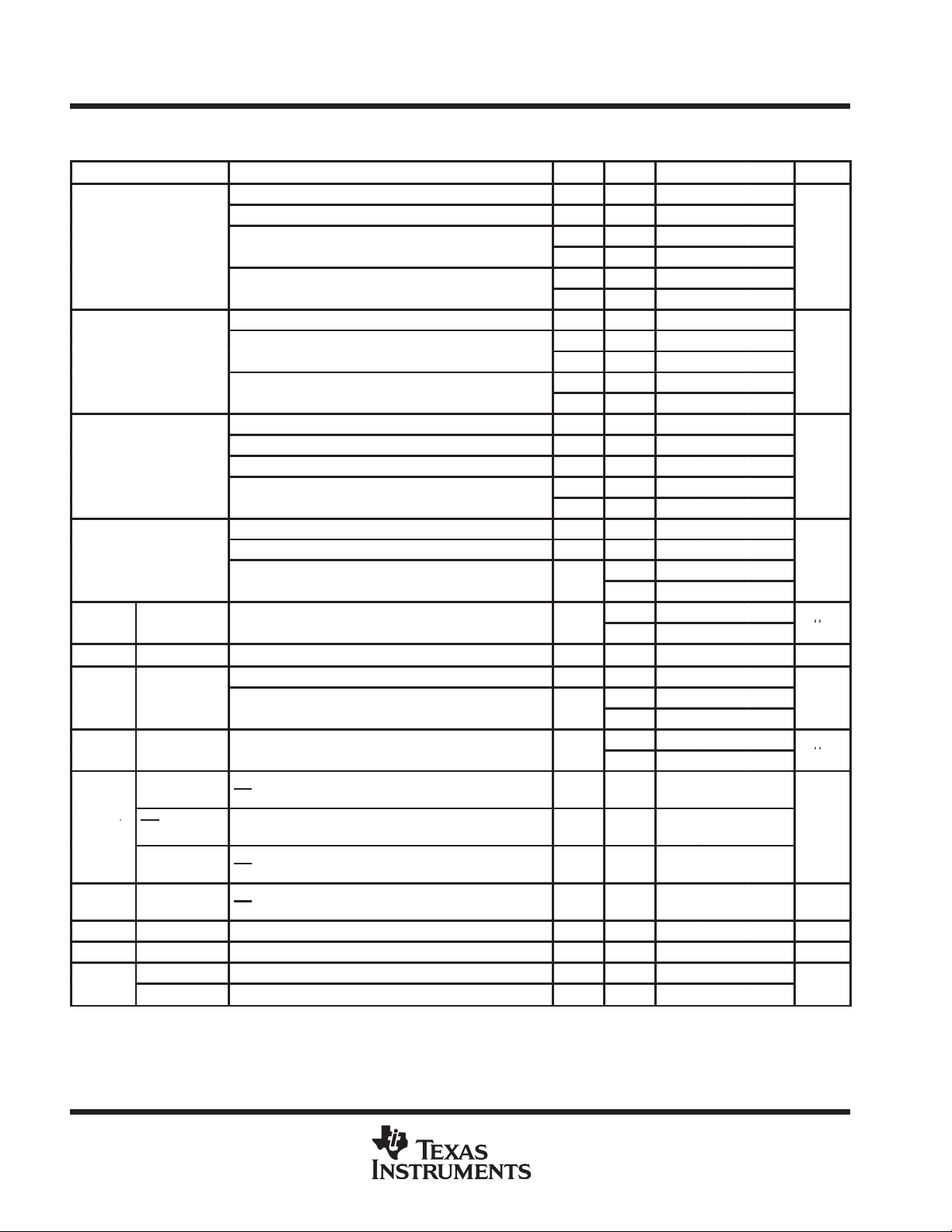
electrical characteristics over recommended operating free-air temperature range (unless
otherwise noted)
PARAMETER TEST CONDITIONS
IOH = –100 µA 3 V 3 V 2.9 3
IOH = –8 mA 2.3 V 3 V 2
OHA
V
OHB
V
OLA
OLB
p
†
I
OZ
I
CCA
CCB
∆I
CCA
∆I
CCB
C
i
C
io
pd
†
For I/O ports, the parameter IOZ includes the input leakage current.
‡
This is the increase in supply current for each input that is at one of the specified voltage levels rather than 0 V or the associated VCC.
A or B ports
B to A
A port
OE
DIR
‡
B port
Control inputs VI = V
A or B ports VO = V
A to B Outputs enabled 3.3 V 5 V 38
B to A Outputs enabled 3.3 V 5 V 36.5
= –12
OH
= –24
OH
IOH = –100 µA 3 V 3 V 2.9 3
= –12
OH
= –24
OH
IOL = 100 µA 3 V 3 V 0.1
IOL = 8 mA 2.3 V 3 V 0.6
IOL = 12 mA 2.7 V 3 V 0.1 0.5
= 24
OL
IOL = 100 µA 3 V 3 V 0.1
IOL = 12 mA 2.3 V 3 V 0.4
= 24
OL
=
I
VO = V
A port = V
p
p
VI = V
OE
VI = V
DIR at V
VI = V
OE
VI = V
OE
or
CCA
or GND, VI = VIL or V
CCA/B
or GND, IO = 0 3.6 V Open 5 50
CCA
=
CCB
=
CCA
– 0.6 V, Other inputs at V
CCA
at GND and DIR at V
– 0.6 V, Other inputs at V
CCA
CCA
– 0.6 V, Other inputs at V
CCA
at GND
– 2.1 V, Other inputs at V
CCB
at GND and DIR at GND
or GND Open Open 4 pF
CCA
or GND 3.3 V 5 V 18.5 pF
CCA/B
or
,
,
CCA
=
O
=
O
CCA
CCA
CCA
CCB
IH
or GND,
or GND,
or GND,
or GND,
V
CCAVCCB
2.7 V 3 V 2.2 2.5
3 V 3 V 2.4 2.8
3 V 3 V 2.2 2.6
2.7 V 4.5 V 2 2.3
2.3 V 3 V 2.4
2.7 V 3 V 2.4 2.8
3 V 3 V 2.2 2.6
2.7 V 4.5 V 3.2 4.2
3 V 3 V 0.2 0.5
2.7 V 4.5 V 0.2 0.5
4.5 V 0.2 0.5
3.6 V ±0.1 ±1
5.5 V ±0.1 ±1
3.6 V 3.6 V ±0.5 ±5 µA
3.6 V 5 50
5.5 V 5 50
3.6 V 5 50
5.5 V 8 80
3.6 V 3.6 V 0.35 0.5
3.6 V 3.6 V 0.35 0.5
3.6 V 3.6 V 0.35 0.5
3.6 V 5.5 V 1 1.5 mA
MIN TYP MAX UNIT
3 V 0.2 0.5
V
V
µ
µA
µ
mA
p
4
POST OFFICE BOX 655303 • DALLAS, TEXAS 75265

(INPUT)
(OUTPUT)
A
B
ns
B
A
ns
OE
A
ns
OE
B
ns
OE
A
ns
OE
B
ns
SN74LVCC3245A
OCTAL BUS TRANSCEIVER WITH ADJUSTABLE OUTPUT VOLTAGE
AND 3-STATE OUTPUTS
SCAS585F – NOVEMBER 1996 – REVISED AUGUST 1998
switching characteristics over recommended operating free-air temperature range (unless
otherwise noted) (see Figures 1 through 4)
V
PARAMETER
t
PHL
t
PLH
t
PHL
t
PLH
t
PZL
t
PZH
t
PZL
t
PZH
t
PLZ
t
PHZ
t
PLZ
t
PHZ
FROM
TO
= 2.5 V ± 0.2 V ,
CCA
V
= 3.3 V ± 0.3 V
CCB
MIN MAX MIN MAX MIN MAX
1 9.4 1 6 1 7.1
1 9.1 1 5.3 1 7.2
1 11.2 1 5.8 1 6.4
1 9.9 1 7 1 7.6
1 14.5 1 9.2 1 9.7
1 12.9 1 9.5 1 9.5
1 13 1 8.1 1 9.2
1 12.8 1 8.4 1 9.9
1 7.1 1 5.5 1 6.6
1 6.9 1 7.8 1 6.9
1 8.8 1 7.3 1 7.5
1 8.9 1 7 1 7.9
V
= 2.7 V TO 3.6 V,
CCA
V
= 5 V ± 0.5 V
CCB
V
= 2.7 V TO 3.6 V,
CCA
V
= 3.3 V ± 0.3 V
CCB
UNIT
POST OFFICE BOX 655303 • DALLAS, TEXAS 75265
5

SN74LVCC3245A
OCTAL BUS TRANSCEIVER WITH ADJUSTABLE OUTPUT VOLTAGE
AND 3-STATE OUTPUTS
SCAS585F – NOVEMBER 1996 – REVISED AUGUST 1998
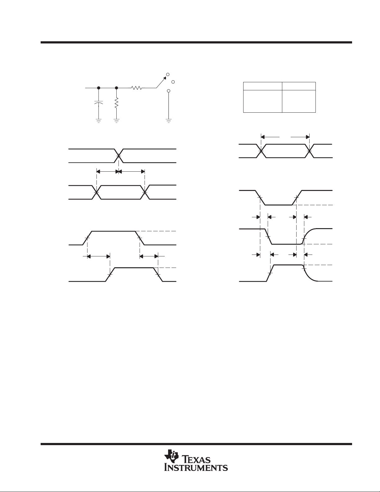
PARAMETER MEASUREMENT INFORMATION FOR A PORT
V
From Output
Under Test
CL = 30 pF
(see Note A)
= 2.5 V ± 0.2 V AND V
CCA
500 Ω
500 Ω
S1
2 × V
Open
GND
CC
= 3.3 V ± 0.3 V
CCB
TEST S1
t
pd
t
PLZ/tPZL
t
PHZ/tPZH
Open
2 × V
GND
CC
LOAD CIRCUIT
Timing
Input
t
Data
Input
Input
t
PLH
Output
NOTES: A. CL includes probe and jig capacitance.
B. Waveform 1 is for an output with internal conditions such that the output is low except when disabled by the output control.
Waveform 2 is for an output with internal conditions such that the output is high except when disabled by the output control.
C. All input pulses are supplied by generators having the following characteristics: PRR ≤ 10 MHz, ZO = 50 Ω, tr ≤ 2 ns, tf ≤ 2 ns.
D. The outputs are measured one at a time with one transition per measurement.
E. t
PLZ
F. t
PZL
G. t
PLH
VCC/2
VOLTAGE WAVEFORMS
SETUP AND HOLD TIMES
VCC/2 VCC/2
VOLTAGE WAVEFORMS
PROPAGATION DELAY TIMES
and t
PHZ
and t
PZH
and t
PHL
VCC/2
t
su
are the same as t
are the same as ten.
are the same as tpd.
h
VCC/2
VCC/2 VCC/2
.
dis
t
PHL
V
0 V
V
0 V
V
0 V
V
V
CC
CC
CC
OH
OL
Input
Output
Control
(low-level
enabling)
Output
Waveform 1
S1 at 2 × V
(see Note B)
Output
Waveform 2
S1 at GND
(see Note B)
VOLTAGE WAVEFORMS
PULSE DURATION
t
PZL
CC
t
PZH
VOLTAGE WAVEFORMS
ENABLE AND DISABLE TIMES
VCC/2
VCC/2
t
w
V
0 V
V
0 V
V
V
V
0 V
CC
CC
CC
OL
OH
VCC/2VCC/2
VCC/2VCC/2
t
PLZ
VOL + 0.15 V
t
PHZ
VOH – 0.15 V
Figure 1. Load Circuit and Voltage Waveforms
6
POST OFFICE BOX 655303 • DALLAS, TEXAS 75265
From Output
Under Test
CL = 50 pF
(see Note A)
OCTAL BUS TRANSCEIVER WITH ADJUSTABLE OUTPUT VOLTAGE
AND 3-STATE OUTPUTS
SCAS585F – NOVEMBER 1996 – REVISED AUGUST 1998
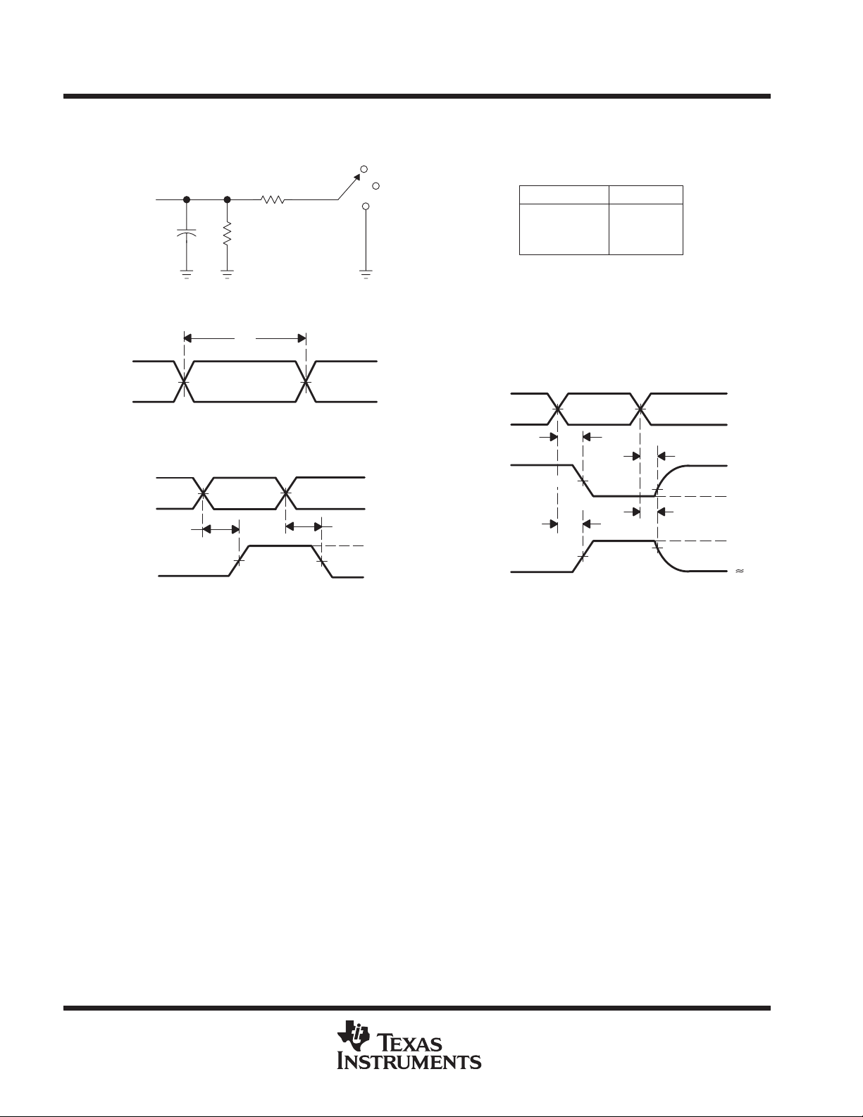
PARAMETER MEASUREMENT INFORMATION FOR B PORT
V
= 2.5 V ± 0.2 V AND V
CCA
500 Ω
500 Ω
S1
2 × V
Open
GND
CC
= 3.3 V ± 0.3 V
CCB
TEST S1
t
pd
t
PLZ/tPZL
t
PHZ/tPZH
SN74LVCC3245A
Open
2 × V
CC
GND
LOAD CIRCUIT
Timing
Input
t
Data
Input
Input
t
PLH
Output
NOTES: A. CL includes probe and jig capacitance.
B. Waveform 1 is for an output with internal conditions such that the output is low except when disabled by the output control.
Waveform 2 is for an output with internal conditions such that the output is high except when disabled by the output control.
C. All input pulses are supplied by generators having the following characteristics: PRR ≤ 10 MHz, ZO = 50 Ω, tr ≤ 2 ns, tf ≤ 2 ns.
D. The outputs are measured one at a time with one transition per measurement.
E. t
PLZ
F. t
PZL
G. t
PLH
VCC/2
VOLTAGE WAVEFORMS
SETUP AND HOLD TIMES
VCC/2 VCC/2
VOLTAGE WAVEFORMS
PROPAGATION DELAY TIMES
and t
PHZ
and t
PZH
and t
PHL
VCC/2
t
su
are the same as t
are the same as ten.
are the same as tpd.
h
VCC/2
VCC/2 VCC/2
.
dis
t
PHL
V
0 V
V
0 V
V
0 V
V
V
CC
CC
CC
OH
OL
Input
Output
Control
(low-level
enabling)
Output
Waveform 1
S1 at 2 × V
(see Note B)
Output
Waveform 2
S1 at GND
(see Note B)
VOLTAGE WAVEFORMS
PULSE DURATION
t
PZL
CC
t
PZH
VOLTAGE WAVEFORMS
ENABLE AND DISABLE TIMES
VCC/2
VCC/2
t
w
V
0 V
V
0 V
V
V
V
0 V
CC
CC
CC
OL
OH
VCC/2VCC/2
VCC/2VCC/2
t
PLZ
VOL + 0.15 V
t
PHZ
VOH – 0.15 V
Figure 2. Load Circuit and Voltage Waveforms
POST OFFICE BOX 655303 • DALLAS, TEXAS 75265
7
SN74LVCC3245A
OCTAL BUS TRANSCEIVER WITH ADJUSTABLE OUTPUT VOLTAGE
AND 3-STATE OUTPUTS
SCAS585F – NOVEMBER 1996 – REVISED AUGUST 1998
PARAMETER MEASUREMENT INFORMATION FOR B PORT
V
From Output
Under Test
CL = 50 pF
(see Note A)
B-Port
Input
Input
B-Port
Output
500 Ω
500 Ω
LOAD CIRCUIT
t
w
50% V
CC
VOLTAGE WAVEFORMS
PULSE DURATION
50% V
1.5 V
CC
1.5 V
t
PLH
50% V
CC
VOLTAGE WAVEFORMS
PROPAGATION DELAY TIMES
NONINVERTING OUTPUTS
= 3.6 V AND V
CCA
2 × V
S1
GND
50% V
CC
V
0 V
t
PHL
V
V
Open
V
0 V
CC
OH
OL
CC
CC
Waveform 1
S1 at 2 × V
(see Note B)
Waveform 2
(see Note B)
= 5.5 V
CCB
Output
Control
Output
CC
Output
S1 at Open
TEST S1
t
PLH/tPHL
t
PLZ/tPZL
t
PHZ/tPZH
1.5 V
t
PZL
50% V
CC
t
PZH
50% V
CC
VOLTAGE WAVEFORMS
ENABLE AND DISABLE TIMES
LOW- AND HIGH-LEVEL ENABLING
t
t
PHZ
PLZ
Open
2 × V
Open
CC
1.5 V
VOL + 0.3 V
VOH – 0.3 V
2.7 V
0 V
V
CC
V
OL
V
OH
[
0 V
NOTES: A. CL includes probe and jig capacitance.
B. Waveform 1 is for an output with internal conditions such that the output is low except when disabled by the output control.
Waveform 2 is for an output with internal conditions such that the output is high except when disabled by the output control.
C. All input pulses are supplied by generators having the following characteristics: PRR ≤ 10 MHz, ZO = 50 Ω, tr ≤ 2.5 ns, tf≤ 2.5 ns.
D. The outputs are measured one at a time with one transition per measurement.
Figure 3. Load Circuit and Voltage Waveforms
8
POST OFFICE BOX 655303 • DALLAS, TEXAS 75265

OCTAL BUS TRANSCEIVER WITH ADJUSTABLE OUTPUT VOLTAGE
PARAMETER MEASUREMENT INFORMATION FOR A AND B PORT
From Output
Under Test
CL = 50 pF
(see Note A)
LOAD CIRCUIT
Input
VOLTAGE WAVEFORMS
PULSE DURATION
Input
t
PLH
Output
PROPAGATION DELAY TIMES
NOTES: A. CL includes probe and jig capacitance.
B. Waveform 1 is for an output with internal conditions such that the output is low except when disabled by the output control.
Waveform 2 is for an output with internal conditions such that the output is high except when disabled by the output control.
C. All input pulses are supplied by generators having the following characteristics: PRR ≤ 10 MHz, ZO = 50 Ω, tr ≤ 2.5 ns, tf≤ 2.5 ns.
D. The outputs are measured one at a time with one transition per measurement.
1.5 V
VOLTAGE WAVEFORMS
NONINVERTING OUTPUTS
500 Ω
500 Ω
t
w
1.5 V
1.5 V 1.5 V
SN74LVCC3245A
AND 3-STATE OUTPUTS
SCAS585F – NOVEMBER 1996 – REVISED AUGUST 1998
V
AND V
CCA
7 V
S1
1.5 V1.5 V
t
PHL
GND
2.7 V
0 V
V
OH
V
OL
Open
2.7 V
0 V
= 3.6 V
CCB
Output
Control
Output
Waveform 1
S1 at 7 V
(see Note B)
Output
Waveform 2
S1 at Open
(see Note B)
TEST S1
t
PLH/tPHL
t
PLZ/tPZL
t
PHZ/tPZH
1.5 V
t
PZL
t
PZH
VOLTAGE WAVEFORMS
ENABLE AND DISABLE TIMES
LOW- AND HIGH-LEVEL ENABLING
t
PLZ
1.5 V
t
PHZ
1.5 V
Open
7 V
Open
1.5 V
VOL + 0.3 V
VOH – 0.3 V
2.7 V
0 V
3.5 V
V
OL
V
OH
[
0 V
Figure 4. Load Circuit and Voltage Waveforms
POST OFFICE BOX 655303 • DALLAS, TEXAS 75265
9

IMPORTANT NOTICE
T exas Instruments and its subsidiaries (TI) reserve the right to make changes to their products or to discontinue
any product or service without notice, and advise customers to obtain the latest version of relevant information
to verify, before placing orders, that information being relied on is current and complete. All products are sold
subject to the terms and conditions of sale supplied at the time of order acknowledgement, including those
pertaining to warranty, patent infringement, and limitation of liability.
TI warrants performance of its semiconductor products to the specifications applicable at the time of sale in
accordance with TI’s standard warranty. Testing and other quality control techniques are utilized to the extent
TI deems necessary to support this warranty . Specific testing of all parameters of each device is not necessarily
performed, except those mandated by government requirements.
CERT AIN APPLICATIONS USING SEMICONDUCTOR PRODUCTS MAY INVOLVE POTENTIAL RISKS OF
DEATH, PERSONAL INJURY, OR SEVERE PROPERTY OR ENVIRONMENTAL DAMAGE (“CRITICAL
APPLICATIONS”). TI SEMICONDUCTOR PRODUCTS ARE NOT DESIGNED, AUTHORIZED, OR
WARRANTED TO BE SUITABLE FOR USE IN LIFE-SUPPORT DEVICES OR SYSTEMS OR OTHER
CRITICAL APPLICA TIONS. INCLUSION OF TI PRODUCTS IN SUCH APPLICATIONS IS UNDERST OOD TO
BE FULLY AT THE CUSTOMER’S RISK.
In order to minimize risks associated with the customer’s applications, adequate design and operating
safeguards must be provided by the customer to minimize inherent or procedural hazards.
TI assumes no liability for applications assistance or customer product design. TI does not warrant or represent
that any license, either express or implied, is granted under any patent right, copyright, mask work right, or other
intellectual property right of TI covering or relating to any combination, machine, or process in which such
semiconductor products or services might be or are used. TI’s publication of information regarding any third
party’s products or services does not constitute TI’s approval, warranty or endorsement thereof.
Copyright 1998, Texas Instruments Incorporated
 Loading...