

Texas Instruments SN74LVC827ADBLE, SN74LVC827ADBR, SN74LVC827ADGVR, SN74LVC827ADW, SN74LVC827ADWR Datasheet
...
SN74LVC827A
10-BIT BUFFER/DRIVER
WITH 3-STATE OUTPUTS
SCAS306G – MARCH 1993 – REVISED JUNE 1998
D
EPIC
(Enhanced-Performance Implanted
CMOS) Submicron Process
D
Typical V
< 0.8 V at V
D
Typical V
> 2 V at V
D
Power Off Disables Outputs, Permitting
(Output Ground Bounce)
OLP
= 3.3 V, TA = 25°C
CC
(Output VOH Undershoot)
OHV
= 3.3 V, TA = 25°C
CC
Live Insertion
D
Supports Mixed-Mode Signal Operation on
All Ports (5-V Input/Output Voltage With
3.3-V V
D
ESD Protection Exceeds 2000 V Per
CC
)
MIL-STD-883, Method 3015; Exceeds 200 V
Using Machine Model (C = 200 pF, R = 0)
D
Latch-Up Performance Exceeds 250 mA Per
JESD 17
D
Package Options Include Plastic
Small-Outline (DW), Shrink Small-Outline
(DB), and Thin Shrink Small-Outline (PW)
Packages
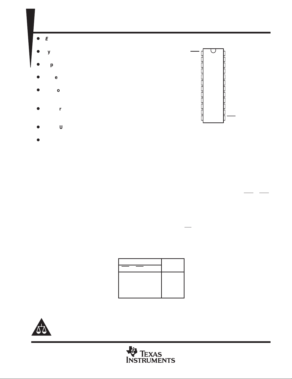
description
DB, DW, OR PW PACKAGE
(TOP VIEW)
1
2
3
4
5
6
7
8
9
10
11
12
24
23
22
21
20
19
18
17
16
15
14
13
V
CC
Y1
Y2
Y3
Y4
Y5
Y6
Y7
Y8
Y9
Y10
OE2
OE1
A1
A2
A3
A4
A5
A6
A7
A8
A9
A10
GND
This 10-bit buffer/bus driver is designed for 1.65-V to 3.6-V VCC operation.
The SN74LVC827A provides a high-performance bus interface for wide data paths or buses carrying parity .
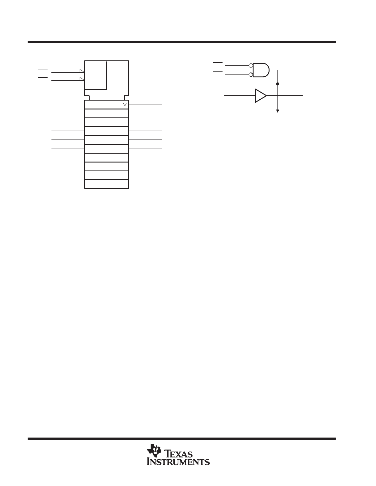
The 3-state control gate is a 2-input AND gate with active-low inputs so that if either output-enable (OE1
or OE2)
input is high, all ten outputs are in the high-impedance state. The SN74LVC827A provides true data at
its outputs.
Inputs can be driven from either 3.3-V or 5-V devices. This feature allows the use of these devices as translators
in a mixed 3.3-V/5-V system environment.
T o ensure the high-impedance state during power up or power down, OE
should be tied to VCC through a pullup
resistor; the minimum value of the resistor is determined by the current-sinking capability of the driver.
The SN74LVC827A is characterized for operation from –40°C to 85°C.
FUNCTION TABLE
INPUTS
OE1 OE2 A
L L L L
L LH H
HXX Z
XHX Z
OUTPUT
Y
Please be aware that an important notice concerning availability, standard warranty, and use in critical applications of
Texas Instruments semiconductor products and disclaimers thereto appears at the end of this data sheet.
EPIC is a trademark of Texas Instruments Incorporated.
PRODUCTION DATA information is current as of publication date.
Products conform to specifications per the terms of Texas Instruments
standard warranty. Production processing does not necessarily include
testing of all parameters.
POST OFFICE BOX 655303 • DALLAS, TEXAS 75265
Copyright 1998, Texas Instruments Incorporated
1
SN74LVC827A
10-BIT BUFFER/DRIVER
WITH 3-STATE OUTPUTS
SCAS306G – MARCH 1993 – REVISED JUNE 1998
1
13
2
3
4
5
6
7
8
9
10
11
†
&
EN
1
23
22
21
20
19
18
17
16
15
14
logic symbol
OE1
OE2
A1
A2
A3
A4
A5
A6
A7
A8
A9
A10
†
This symbol is in accordance with ANSI/IEEE Std 91-1984 and
IEC Publication 617-12.
logic diagram (positive logic)
1
OE1
13
OE2
223
A1
Y1
Y2
Y3
Y4
Y5
Y6
Y7
Y8
Y9
Y10
Y1
To Nine Other Channels
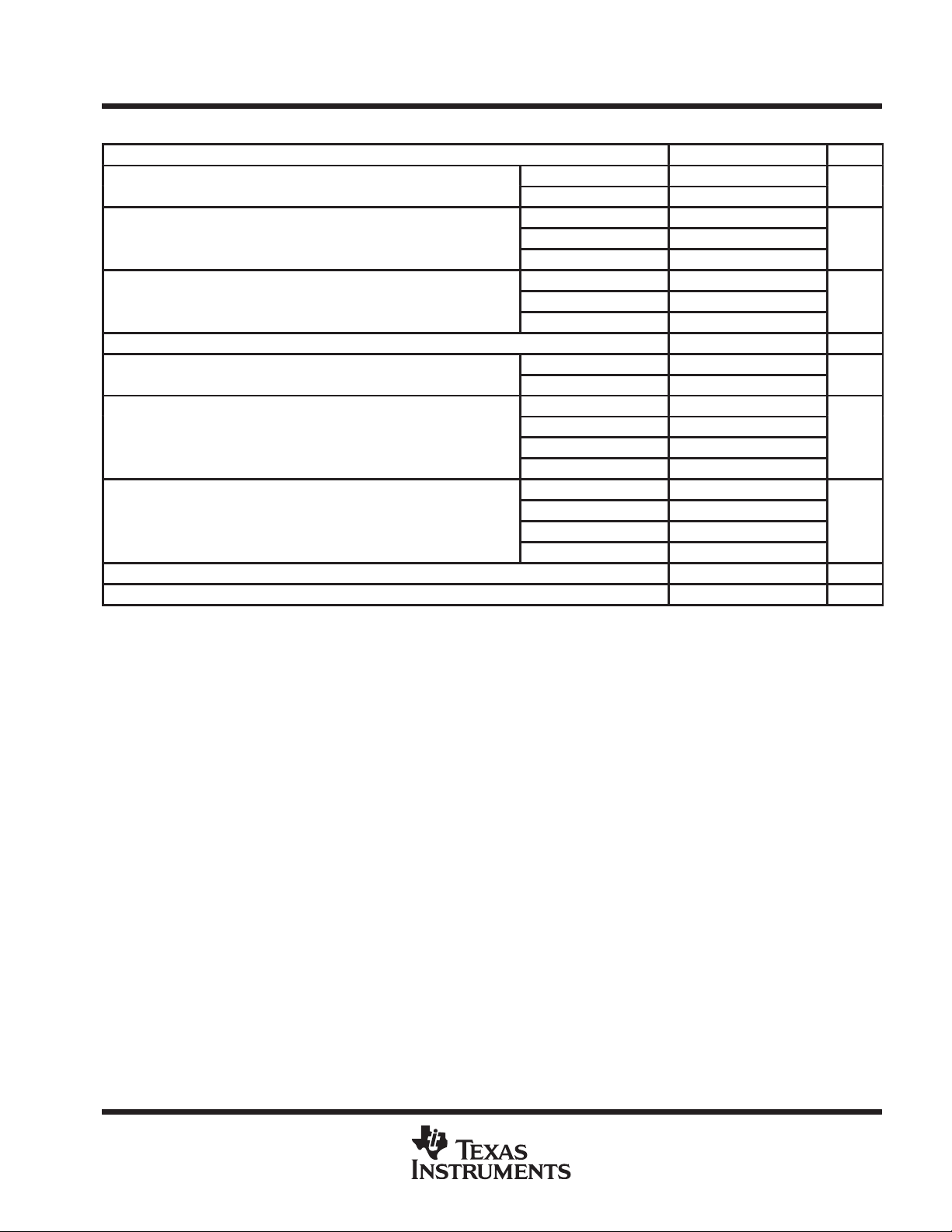
absolute maximum ratings over operating free-air temperature range (unless otherwise noted)
‡
Supply voltage range, V
Input voltage range, V
Voltage range applied to any output in the high-impedance or power-off state, V
–0.5 V to 6.5 V. . . . . . . . . . . . . . . . . . . . . . . . . . . . . . . . . . . . . . . . . . . . . . . . . . . . . . . . .
CC
(see Note 1) –0.5 V to 6.5 V. . . . . . . . . . . . . . . . . . . . . . . . . . . . . . . . . . . . . . . . . . . . . . . . .
I
O
(see Note 1) –0.5 V to 6.5 V. . . . . . . . . . . . . . . . . . . . . . . . . . . . . . . . . . . . . . . . . . . . . . . . . . . . . . . . . . . . . . . . . . .
Voltage range applied to any output in the high or low state, V
O
(see Notes 1 and 2) –0.5 V to VCC + 0.5 V. . . . . . . . . . . . . . . . . . . . . . . . . . . . . . . . . . . . . . . . . . . . . . . . . . . . . . .
Input clamp current, I
Output clamp current, I
Continuous output current, I
Continuous current through V
Package thermal impedance, θ
(VI < 0 ) –50 mA. . . . . . . . . . . . . . . . . . . . . . . . . . . . . . . . . . . . . . . . . . . . . . . . . . . . . . . . . .
IK
(VO < 0) –50 mA. . . . . . . . . . . . . . . . . . . . . . . . . . . . . . . . . . . . . . . . . . . . . . . . . . . . . . . .
OK
±50 mA. . . . . . . . . . . . . . . . . . . . . . . . . . . . . . . . . . . . . . . . . . . . . . . . . . . . . . . . . . . . .
O
or GND ±100 mA. . . . . . . . . . . . . . . . . . . . . . . . . . . . . . . . . . . . . . . . . . . . . . . . . .
CC
(see Note 3): DB package 104°C/W. . . . . . . . . . . . . . . . . . . . . . . . . . . . . . . .
JA
DW package 81°C/W. . . . . . . . . . . . . . . . . . . . . . . . . . . . . . . . .
PW package 120°C/W. . . . . . . . . . . . . . . . . . . . . . . . . . . . . . . .
Storage temperature range, T
‡
Stresses beyond those listed under “absolute maximum ratings” may cause permanent damage to the device. These are stress ratings only, and
functional operation of the device at these or any other conditions beyond those indicated under “recommended operating conditions” is not
implied. Exposure to absolute-maximum-rated conditions for extended periods may affect device reliability.
NOTES: 1. The input negative-voltage and output voltage ratings may be exceeded if the input and output current ratings are observed.
2. The value of VCC is provided in the recommended operating conditions table.
3. The package thermal impedance is calculated in accordance with JESD 51.
–65°C to 150°C. . . . . . . . . . . . . . . . . . . . . . . . . . . . . . . . . . . . . . . . . . . . . . . . . . .
stg
2
POST OFFICE BOX 655303 • DALLAS, TEXAS 75265
VCCSuppl
oltage
V
VOOutput voltage
V
IOHHigh-level output current
mA
IOLLow-level output current
mA
SN74LVC827A
10-BIT BUFFER/DRIVER
WITH 3-STATE OUTPUTS
SCAS306G – MARCH 1993 – REVISED JUNE 1998
recommended operating conditions (see Note 4)
MIN MAX UNIT
pp
y v
V
V
V
∆t/∆v Input transition rise or fall rate 0 10 ns/V
T
NOTE 4: All unused inputs of the device must be held at VCC or GND to ensure proper device operation. Refer to the TI application report,
High-level input voltage
IH
Low-level input voltage
IL
Input voltage 0 5.5 V
I
p
p
p
Operating free-air temperature –40 85 °C
A
Implications of Slow or Floating CMOS Inputs
, literature number SCBA004.
Operating 1.65 3.6
Data retention only 1.5
VCC = 1.65 V to 1.95 V 0.65 × V
VCC = 2.3 V to 2.7 V
VCC = 2.7 V to 3.6 V 2
VCC = 1.65 V to 1.95 V 0.35 × V
VCC = 2.3 V to 2.7 V 0.7
VCC = 2.7 V to 3.6 V 0.8
High or low state 0 V
3 state 0 5.5
VCC = 1.65 V –4
VCC = 2.3 V –8
VCC = 2.7 V –12
VCC = 3 V –24
VCC = 1.65 V 4
VCC = 2.3 V 8
VCC = 2.7 V 12
VCC = 3 V 24
CC
1.7
CC
V
CC
V
POST OFFICE BOX 655303 • DALLAS, TEXAS 75265
3
 Loading...