

Datasheet SN74LVC1G17DBVR, SN74LVC1G17DCKR, SN74LVC1G17DRLR, SN74LVC1G17DRY2, SN74LVC1G17DSF2 Datasheet (Texas Instruments) [ru]
...
Product
Folder
Sample &
Buy
Technical
Documents
Tools &
Software
Support &
Community
SN74LVC1G17 Single Schmitt-Trigger Buffer
1 Features 3 Description
1
• Available in Ultra Small 0.64-mm
2
Package (DPW) With 0.5-mm Pitch
• Supports 5-V VCCOperation
• Inputs Accept Voltages to 5.5 V
• Max tpdof 4.6 ns at 3.3 V
• Low Power Consumption, 10-μA Max I
CC
• ±24-mA Output Drive at 3.3 V
• I
Supports Live Insertion, Partial-Power-Down
off
Mode, and Back-Drive Protection
• Latch-Up Performance Exceeds 100 mA Per
JESD 78, Class II
• ESD Protection Exceeds JESD 22
– 2000-V Human-Body Model (A114-A)
– 200-V Machine Model (A115-A)
– 1000-V Charged-Device Model (C101)
2 Applications
• AV Receiver
• Audio Dock: Portable
• Blu-ray Player and Home Theater
• MP3 Player/Recorder
• Personal Digital Assistant (PDA)
• Power: Telecom/Server AC/DC Supply: Single
Controller: Analog and Digital
• Solid State Drive (SSD): Client and Enterprise
• TV: LCD/Digital and High-Definition (HDTV)
• Tablet: Enterprise
• Video Analytics: Server
• Wireless Headset, Keyboard, and Mouse
This single Schmitt-trigger buffer is designed for
1.65-V to 5.5-V VCCoperation.
The SN74LVC1G17 device contains one buffer and
performs the Boolean function Y = A.
The CMOS device has high output drive while
maintaining low static power dissipation over a broad
Vcc operating range.
The SN74LVC1G17 is available in a variety of
packages, including the ultra-small DPW package
with a body size of 0.8 mm × 0.8mm.
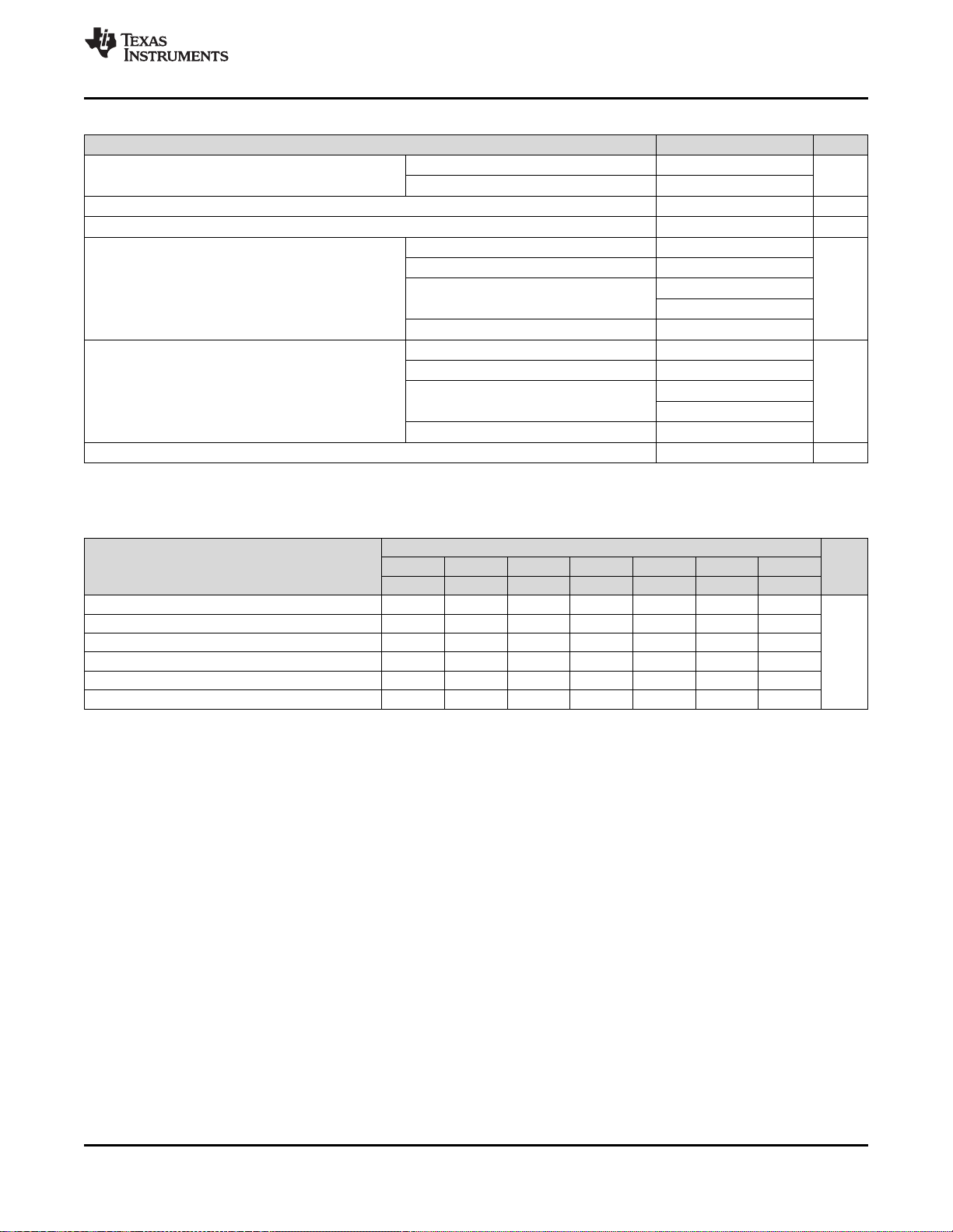
Device Information
DEVICE NAME PACKAGE BODY SIZE
SN74LVC1G17 X2SON (4) 0.8mm × 0.8mm
(1) For all available packages, see the orderable addendum at
the end of the datasheet.
SN74LVC1G17
SCES351V –JULY 2001–REVISED APRIL 2014
(1)
SOT-23 (5) 2.9mm × 1.6mm
SC70 (5) 2.0mm × 1.25mm
SON (6) 1.45mm × 1.0mm
SON (6) 1.0mm × 1.0mm
4 Simplified Schematic
1
An IMPORTANT NOTICE at the end of this data sheet addresses availability, warranty, changes, use in safety-critical applications,
intellectual property matters and other important disclaimers. PRODUCTION DATA.
SN74LVC1G17
SCES351V –JULY 2001–REVISED APRIL 2014
www.ti.com
Table of Contents
1 Features.................................................................. 1 9 Detailed Description............................................ 10
2 Applications ........................................................... 1
3 Description ............................................................. 1
4 Simplified Schematic............................................. 1
5 Revision History..................................................... 2
6 Pin Configuration and Functions......................... 3
7 Specifications......................................................... 4
7.1 Absolute Maximum Ratings ..................................... 4
7.2 Handling Ratings....................................................... 4
7.3 Recommended Operating Conditions ...................... 5
7.4 Thermal Information.................................................. 5
7.5 Electrical Characteristics—DC Limit Changes.......... 6
7.6 Switching Characteristics, CL= 15 pF ...................... 7
7.7 Switching Characteristics AC Limit, –40°C TO 85°C 7
7.8 Switching Characteristics AC Limit, –40°C TO
125°C......................................................................... 7
7.9 Operating Characteristics.......................................... 7
7.10 Typical Characteristics............................................ 7 Information........................................................... 13
8 Parameter Measurement Information .................. 8
9.1 Overview ................................................................. 10
9.2 Functional Block Diagram....................................... 10
9.3 Feature Description................................................. 10
9.4 Device Functional Modes........................................ 10
10 Applications and Implementation...................... 11
10.1 Application Information.......................................... 11
10.2 Typical Application ............................................... 11
11 Power Supply Recommendations ..................... 12
12 Layout................................................................... 12
12.1 Layout Guidelines ................................................. 12
12.2 Layout Example .................................................... 12
13 Device and Documentation Support................. 13
13.1 Trademarks........................................................... 13
13.2 Electrostatic Discharge Caution............................ 13
13.3 Glossary................................................................ 13
14 Mechanical, Packaging, and Orderable
5 Revision History
Changes from Revision U (February 2014) to Revision V Page
• Added Pin Functions table. .................................................................................................................................................... 3
• Added Handling Ratings table. .............................................................................................................................................. 4
• Added Thermal Information table. ......................................................................................................................................... 5
• Added Typical Characteristics. .............................................................................................................................................. 7
• Added Detailed Description section. .................................................................................................................................... 10
• Added Application and Implementation section. ................................................................................................................. 11
• Added Power Supply Recommendations section. .............................................................................................................. 12
• Added Layout section. ......................................................................................................................................................... 12
Changes from Revision T (November 2012) to Revision U Page
• Added Applications................................................................................................................................................................. 1
• Moved T
• Changed MAX operating free-air temperature from 85°C to 125°C....................................................................................... 5
• Added –40°C to 125°C to Electrical Characteristics table...................................................................................................... 6
• Added Switching Characteristics table for –40°C to 125°C temperature range..................................................................... 7
Changes from Revision S (June 2011) to Revision T Page
to Handling Ratings table..................................................................................................................................... 4
stg
• Removed Ordering Information table. .................................................................................................................................... 3
2 Submit Documentation Feedback Copyright © 2001–2014, Texas Instruments Incorporated
Product Folder Links: SN74LVC1G17
N.C. – No internal connection
See mechanical drawings for dimensions.
DNU – Do not use
DBV PACKAGE
(TOP VIEW)
2
5
3
4
Y
1
A
GND
N.C.
V
CC
DCK PACKAGE
(TOP VIEW)
3
4
2
Y
1
GND
A
N.C.
5
V
CC
DRL PACKAGE
(TOP VIEW)
2
A
1
N.C.
3
4
GND
Y
5
V
CC
DRY PACKAGE
(TOP VIEW)
A
N.C.
N.C.
6
5
4
2
3
GND
Y
V
CC
1
N.C.
GND
DSF PACKAGE
(TOP VIEW)
A
V
CC
Y
N.C.
6
5
4
2
3
1
1 5
2
3
A
GND
Y
V
CC
DPW PACKAGE
(TOP VIEW)
N.C.
4
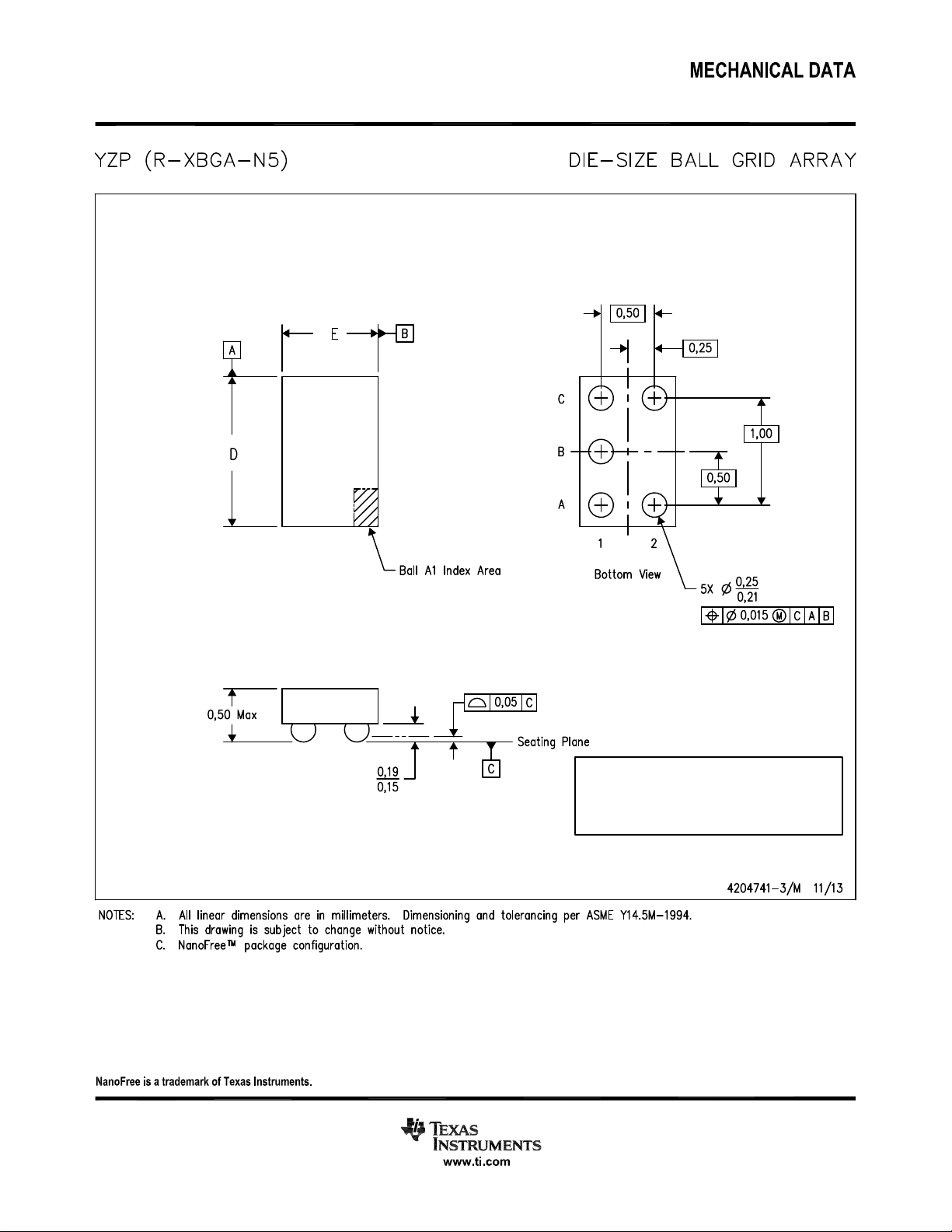
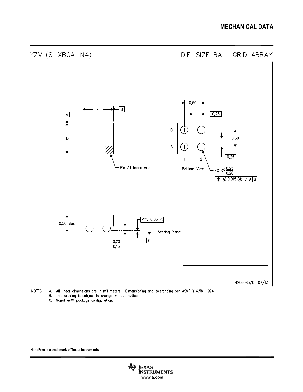
YZV PACKAGE
(TOP VIEW)
A
GND Y
V
CC
A1
A2
B1 B2
YZP PACKAGE
(TOP VIEW)
A
GND
DNU
V
CC
Y
C2C1
B1 B2
A1 A2
www.ti.com
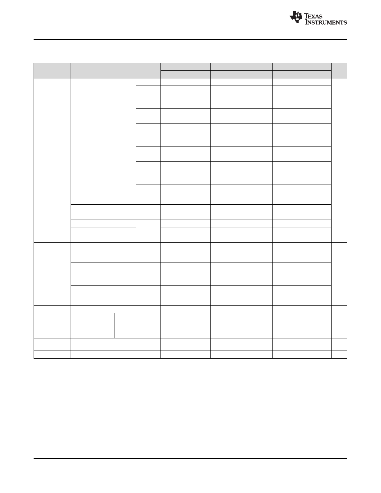
6 Pin Configuration and Functions
Pin Functions
PIN
NAME DRY, DSF YZP YZV
DBV, DCK,
DRL, DPW
NC 1 1, 5 A1, B2 – Not connected
A 2 2 B1 A1 Input
GND 3 3 C1 B1 Ground
Y 4 4 C2 B2 Output
V
CC
5 6 A2 A2 Power terminal
DESCRIPTION
SN74LVC1G17
SCES351V –JULY 2001–REVISED APRIL 2014
Copyright © 2001–2014, Texas Instruments Incorporated Submit Documentation Feedback 3
Product Folder Links: SN74LVC1G17
SN74LVC1G17
SCES351V –JULY 2001–REVISED APRIL 2014
7 Specifications
www.ti.com
7.1 Absolute Maximum Ratings
(1)
over operating free-air temperature range (unless otherwise noted)
MIN MAX UNIT
V
V
V
V
I
IK
I
OK
I
O
Supply voltage range –0.5 6.5 V
CC
Input voltage range
I
Voltage range applied to any output in the high-impedance or power-off state
O
Voltage range applied to any output in the high or low state
O
(2)
(2)
(2)(3)
–0.5 6.5 V
–0.5 6.5 V
–0.5 VCC+ 0.5 V
Input clamp current VI< 0 –50 mA
Output clamp current VO< 0 –50 mA
Continuous output current ±50 mA
Continuous current through VCCor GND ±100 mA
(1) Stresses beyond those listed under Absolute Maximum Ratings may cause permanent damage to the device. These are stress ratings
only, and functional operation of the device at these or any other conditions beyond those indicated under Recommended Operating
Conditions tables is not implied. Exposure to absolute-maximum-rated conditions for extended periods may affect device reliability.
(2) The input and output negative-voltage ratings may be exceeded if the input and output current ratings are observed.
(3) The value of VCCis provided in the Recommended Operating Conditions table.
7.2 Handling Ratings
MIN MAX UNIT
T
stg
(1)
V
ESD
(1) Electrostatic discharge (ESD) to measure device sensitivity and immunity to damage caused by assembly line electrostatic discharges in
to the device.
(2) Level listed above is the passing level per ANSI, ESDA, and JEDEC JS-001. JEDEC document JEP155 states that 500-V HBM allows
safe manufacturing with a standard ESD control process.
(3) Level listed above is the passing level per EIA-JEDEC JESD22-C101. JEDEC document JEP157 states that 250-V CDM allows safe
manufacturing with a standard ESD control process.
Storage temperature range –65 150 °C
Human-Body Model (HBM)
Charged-Device Model (CDM)
(2)
(3)
0 2 kV
0 1 kV
4 Submit Documentation Feedback Copyright © 2001–2014, Texas Instruments Incorporated
Product Folder Links: SN74LVC1G17
www.ti.com
SN74LVC1G17
SCES351V –JULY 2001–REVISED APRIL 2014
7.3 Recommended Operating Conditions
(1)
MIN MAX UNIT
V
V
V
Supply voltage V
CC
Input voltage 0 5.5 V
I
Output voltage 0 V
O
Operating 1.65 5.5
Data retention only 1.5
CC
VCC= 1.65 V –4
VCC= 2.3 V –8
I
High-level output current –16 mA
OH
VCC= 3 V
–24
VCC= 4.5 V –32
VCC= 1.65 V 4
VCC= 2.3 V 8
I
Low-level output current 16 mA
OL
VCC= 3 V
24
VCC= 4.5 V 32
T
Operating free-air temperature –40 125 °C
A
(1) All unused inputs of the device must be held at VCCor GND to ensure proper device operation. Refer to the TI application report,
Implications of Slow or Floating CMOS Inputs, literature number SCBA004.
7.4 Thermal Information
(1)
DBV DCK DRL DRY YZP DPW YZV UNIT
5 PINS 5 PINS 5 PINS 6 PINS 5 PINS 4 PINS 4 PINS
R
θJA
R
θJC(top)
R
θJB
ψ
JT
ψ
JB
R
θJC(bot)
THERMAL METRIC
Junction-to-ambient thermal resistance 229 280 350 608 130 340 181
Junction-to-case (top) thermal resistance 164 66 121 432 54 215 1
Junction-to-board thermal resistance 62 67 171 446 51 294 39
Junction-to-top characterization parameter 44 2 11 191 1 41 8
Junction-to-board characterization parameter 62 66 169 442 50 294 38
Junction-to-case (bottom) thermal resistance – – – 198 – 250 –
(1) For more information about traditional and new thermal metrics, see the IC Package Thermal Metrics application report, SPRA953.
SN74LVC1G17
V
°C/W
Copyright © 2001–2014, Texas Instruments Incorporated Submit Documentation Feedback 5
Product Folder Links: SN74LVC1G17
SN74LVC1G17
SCES351V –JULY 2001–REVISED APRIL 2014
www.ti.com
7.5 Electrical Characteristics—DC Limit Changes
over recommended operating free-air temperature range (unless otherwise noted)
PARAMETER TEST CONDITIONS V
CC
1.65 V 0.76 1.13 0.76 1.13
V
T+
(Positive-going
input threshold
voltage)
2.3 V 1.08 1.56 1.08 1.56
3 V 1.48 1.92 1.48 1.92 V
4.5 V 2.19 2.74 2.19 2.74
5.5 V 2.65 3.33 2.65 3.33
1.65 V 0.35 0.59 0.35 0.59
V
T–
(Negative-going
input threshold
voltage)
2.3 V 0.56 0.88 0.56 0.88
3 V 0.89 1.2 0.89 1.2 V
4.5 V 1.51 1.97 1.51 1.97
5.5 V 1.88 2.4 1.88 2.4
1.65 V 0.36 0.64 0.36 0.64
ΔV
T
Hysteresis 3 V 0.51 0.83 0.51 0.83 V
(VT+– VT–)
2.3 V 0.45 0.78 0.45 0.78
4.5 V 0.58 0.93 0.58 0.93
5.5 V 0.69 1.04 0.69 1.04
IOH= –100 μA VCC– 0.1 VCC– 0.1
1.65 V to
5.5 V
IOH= –4 mA 1.65 V 1.2 1.2
V
OH
IOH= –8 mA 2.3 V 1.9 1.9
IOH= –16 mA 2.4 2.4
IOH= –24 mA 2.3 2.3
3 V
IOH= –32 mA 4.5 V 3.8 3.8
IOL= 100 μA 0.1 0.1
1.65 V to
5.5 V
IOL= 4 mA 1.65 V 0.45 0.45
V
OL
IOL= 8 mA 2.3 V 0.3 0.3
IOL= 16 mA 0.4 0.4
IOL= 24 mA 0.55 0.55
3 V
IOL= 32 mA 4.5 V 0.55 0.55
I
A input VI= 5.5 V or GND ±5 ±5 μA
I
I
off
VIor VO= 5.5 V 0 ±10 ±10 μA
VI= 5.5 V or GND, 10 10
I
CC
IO= 0 μA
VI= 3.6 V or GND, 0.5 1.5
ΔI
CC
C
I
One input at VCC– 0.6 V, 3 V to
Other inputs at VCCor GND 5.5 V
VI= VCCor GND 3.3 V 4.5 pF
0 to
5.5 V
1.65 V to
5.5 V
3 V to
3.6 V
(1) All typical values are at VCC= 3.3 V, TA= 25°C.
25°C –40°C TO 85°C –40°C TO 125°C
MIN TYP
(1)
MAX MIN TYP
(1)
MAX MIN TYP MAX
500 500 μA
UNIT
V
V
6 Submit Documentation Feedback Copyright © 2001–2014, Texas Instruments Incorporated
Product Folder Links: SN74LVC1G17
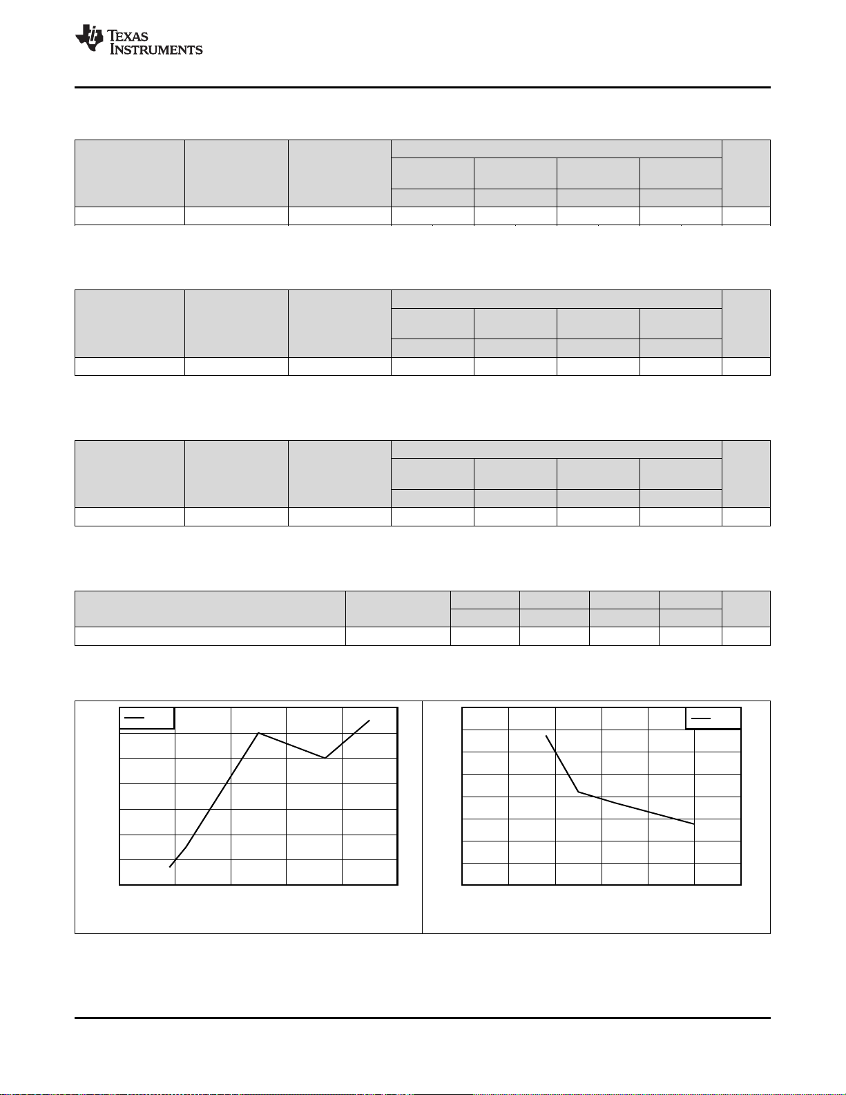
Temperature - °C
TPD - ns
-100 -50 0 50 100 150
3.1
3.2
3.3
3.4
3.5
3.6
3.7
3.8
D001
TPD
Vcc - V
TPD - ns
0 1 2 3 4 5 6
0
1
2
3
4
5
6
7
8
D002
TPD
SN74LVC1G17
www.ti.com
SCES351V –JULY 2001–REVISED APRIL 2014
7.6 Switching Characteristics, CL= 15 pF
over recommended operating free-air temperature range, CL= 15 pF (unless otherwise noted) (see Figure 3 )
–40°C TO 85°C
PARAMETER UNIT
t
pd
FROM TO VCC= 1.8 V VCC= 2.5 V VCC= 3.3 V VCC= 5 V
(INPUT) (OUTPUT) ± 0.15 V ± 0.2 V ± 0.3 V ± 0.5 V
MIN MAX MIN MAX MIN MAX MIN MAX
A Y 2.8 9.9 1.6 5.5 1.5 4.6 0.9 4.4 ns
7.7 Switching Characteristics AC Limit, –40°C TO 85°C
over recommended operating free-air temperature range, CL= 30 pF or 50 pF (unless otherwise noted) (see Figure 4)
–40°C TO 85°C
PARAMETER UNIT
t
pd
FROM TO VCC= 1.8 V VCC= 2.5 V VCC= 3.3 V VCC= 5 V
(INPUT) (OUTPUT) ± 0.15 V ± 0.2 V ± 0.3 V ± 0.5 V
MIN MAX MIN MAX MIN MAX MIN MAX
A Y 3.8 11 2 6.5 1.8 5.5 1.2 5 ns
7.8 Switching Characteristics AC Limit, –40°C TO 125°C
over recommended operating free-air temperature range, CL= 30 pF or 50 pF (unless otherwise noted) (see Figure 4)
–40°C TO 125°C
PARAMETER UNIT
t
pd
FROM TO VCC= 1.8 V VCC= 2.5 V VCC= 3.3 V VCC= 5 V
(INPUT) (OUTPUT) ± 0.15 V ± 0.2 V ± 0.3 V ± 0.5 V
MIN MAX MIN MAX MIN MAX MIN MAX
A Y 3.8 13 2 8 1.8 6.5 1.2 6 ns
7.9 Operating Characteristics
TA= 25°C
PARAMETER UNIT
C
Power dissipation capacitance f = 10 MHz 20 21 22 26 pF
pd
7.10 Typical Characteristics
Figure 1. Across Temperature at 3.3V Vcc Figure 2. Across Vcc at 25°C
Copyright © 2001–2014, Texas Instruments Incorporated Submit Documentation Feedback 7
TEST
VCC= 1.8 V VCC= 2.5 V VCC= 3.3 V VCC= 5 V
CONDITIONS
Product Folder Links: SN74LVC1G17
TYP TYP TYP TYP
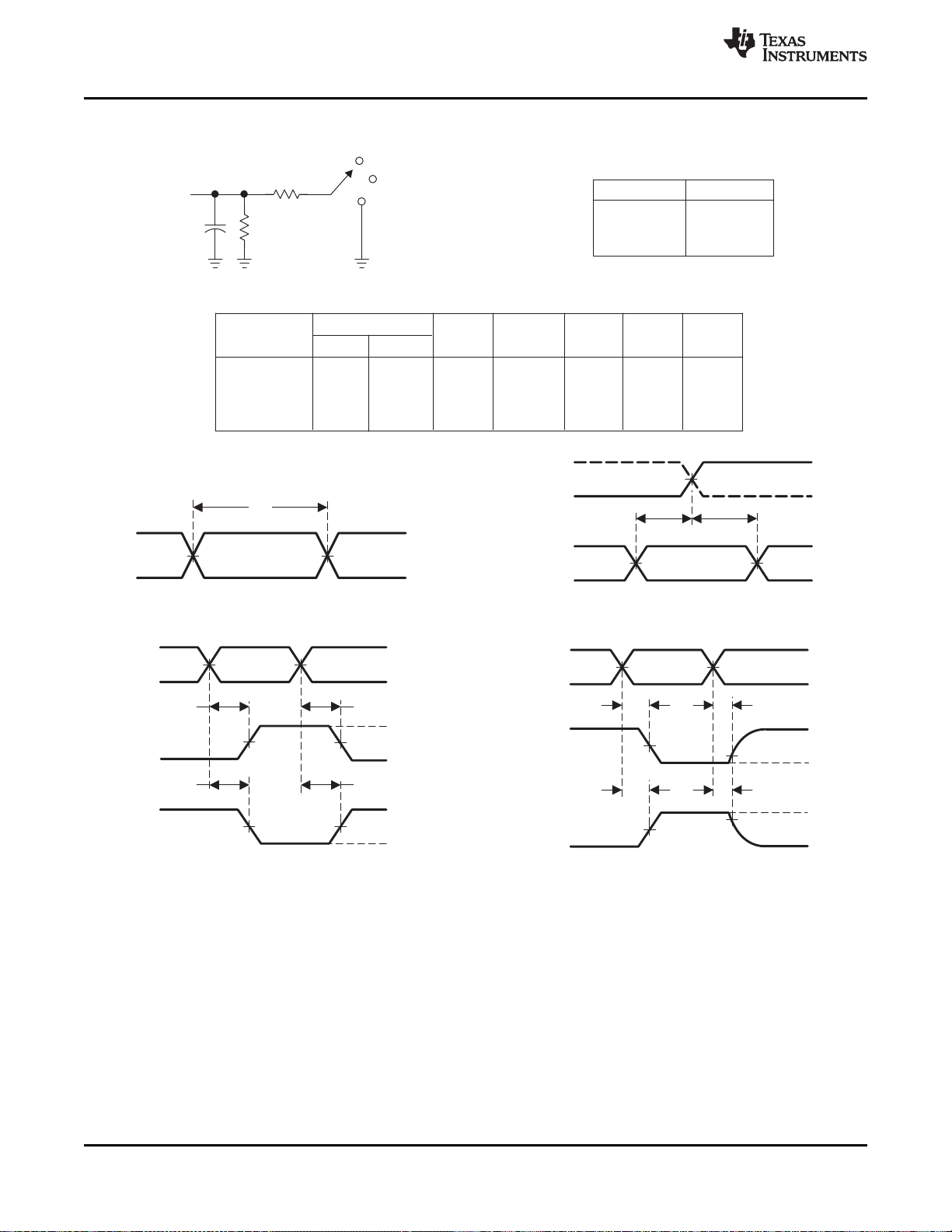
t
h
t
su
FromOutput
UnderTest
C
(seeNote A)
L
LOADCIRCUIT
S1
V
LOAD
Open
GND
R
L
DataInput
TimingInput
0V
0V
0V
t
W
Input
0V
Input
Output
Waveform1
S1atV
(seeNoteB)
LOAD
Output
Waveform2
S1atGND
(seeNoteB)
V
OL
V
OH
0V
»0V
Output
Output
t /t
PLH PHL
Open
TEST S1
Output
Control
V
M
V
M
V
M
V
M
V
M
1.8V 0.15V±
2.5V 0.2V±
3.3V 0.3V±
5V 0.5V±
1MW
1MW
1MW
1MW
V
CC
R
L
2× V
CC
2× V
CC
6V
2× V
CC
V
LOAD
C
L
15pF
15pF
15pF
15pF
0.15V
0.15V
0.3V
0.3V
V
D
3V
V
I
VCC/2
VCC/2
1.5V
VCC/2
V
M
£2ns
£2ns
£2.5ns
£2.5ns
INPUTS
R
L
t /t
r f
V
CC
V
CC
V
CC
V
LOAD
t /t
PLZ PZL
GND
t /t
PHZ PZH
VOLTAGEWAVEFORMS
ENABLE ANDDISABLETIMES
LOW- ANDHIGH-LEVEL ENABLING
VOLTAGEWAVEFORMS
PROPAGATIONDELAY TIMES
INVERTING ANDNONINVERTINGOUTPUTS
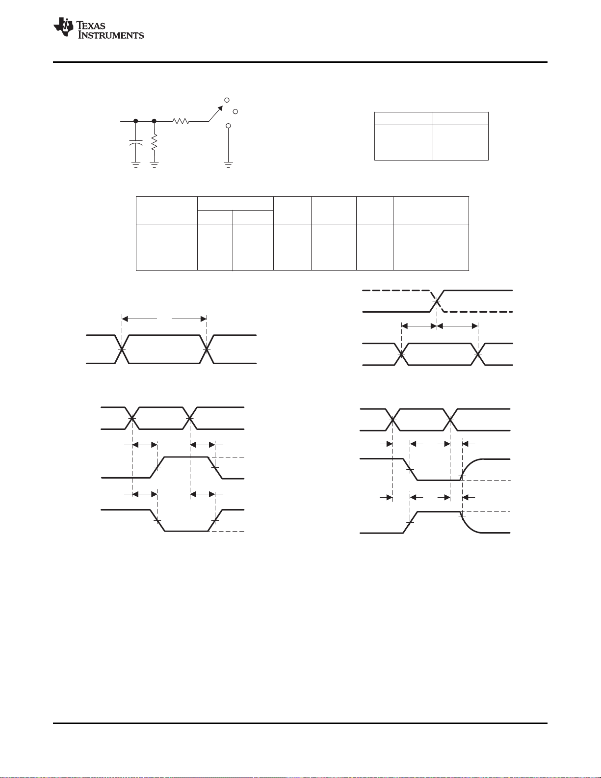
NOTES: A. C includesprobeandjigcapacitance.
B. Waveform1isforanoutputwithinternalconditionssuchthattheoutputislow,exceptwhendisabledbytheoutputcontrol.
Waveform2isforanoutputwithinternalconditionssuchthattheoutputishigh,exceptwhendisabledbytheoutputcontrol.
C. Allinputpulsesaresuppliedbygeneratorshavingthefollowingcharacteristics:PRR 10MHz,Z =50 .
D. Theoutputsaremeasuredoneatatime,withonetransitionpermeasurement.
E. t andt arethesameast .
F. t andt arethesameast .
G. t andt arethesameast .
H. Allparametersandwaveformsarenotapplicabletoalldevices.
L
O
PLZ PHZ dis
PZL PZH en
PLH PHL pd
£ W
VOLTAGEWAVEFORMS
PULSEDURATION
VOLTAGEWAVEFORMS
SETUP ANDHOLDTIMES
V
I
V
I
V
I
V
M
V
M
V /2
LOAD
t
PZL
t
PLZ
t
PHZ
t
PZH
V – V
OH D
V +V
OL D
V
M
V
M
V
M
V
M
V
OL
V
OH
V
I
V
I
V
OH
V
OL
V
M
V
M
V
M
V
M
t
PLH
t
PHL
t
PLH
t
PHL
SN74LVC1G17
SCES351V –JULY 2001–REVISED APRIL 2014
8 Parameter Measurement Information
www.ti.com
Figure 3. Load Circuit and Voltage Waveforms
8 Submit Documentation Feedback Copyright © 2001–2014, Texas Instruments Incorporated
Product Folder Links: SN74LVC1G17
t
h
t
su
FromOutput
UnderTest
C
(seeNote A)
L
LOADCIRCUIT
S1
V
LOAD
Open
GND
R
L
DataInput
TimingInput
0V
0V
0V
t
W
Input
0V
Input
Output
Waveform1
S1atV
(seeNoteB)
LOAD
Output
Waveform2
S1atGND
(seeNoteB)
V
OL
V
OH
0V
»0V
Output
Output
TEST S1
t /t
PLH PHL
Open
Output
Control
V
M
V
M
V
M
V
M
V
M
1.8V 0.15V±
2.5V 0.2V±
3.3V 0.3V±
5V 0.5V±
1kW
500 W
500 W
500 W
V
CC
R
L
2× V
CC
2× V
CC
6V
2× V
CC
V
LOAD
C
L
30pF
30pF
50pF
50pF
0.15V
0.15V
0.3V
0.3V
V
D
3V
V
I
VCC/2
VCC/2
1.5V
VCC/2
V
M
£2ns
£2ns
£2.5ns
£2.5ns
INPUTS
R
L
t /t
r f
V
CC
V
CC
V
CC
V
LOAD
t /t
PLZ PZL
GND
t /t
PHZ PZH
VOLTAGEWAVEFORMS
ENABLE ANDDISABLETIMES
LOW- ANDHIGH-LEVEL ENABLING
VOLTAGEWAVEFORMS
PROPAGATIONDELAY TIMES
INVERTING ANDNONINVERTINGOUTPUTS
NOTES: A. C includesprobeandjigcapacitance.
B. Waveform1isforanoutputwithinternalconditionssuchthattheoutputislow,exceptwhendisabledbytheoutputcontrol.
Waveform2isforanoutputwithinternalconditionssuchthattheoutputishigh,exceptwhendisabledbytheoutputcontrol.
C. Allinputpulsesaresuppliedbygeneratorshavingthefollowingcharacteristics:PRR 10MHz,Z =50 .
D. Theoutputsaremeasuredoneatatime,withonetransitionpermeasurement.
E. t andt arethesameast .
F. t andt arethesameast .
G. t andt arethesameast .
H. Allparametersandwaveformsarenotapplicabletoalldevices.
L
O
PLZ PHZ dis
PZL PZH en
PLH PHL pd
£ W
VOLTAGEWAVEFORMS
PULSEDURATION
VOLTAGEWAVEFORMS
SETUP ANDHOLDTIMES
V
I
V
I
V
I
V
M
V
M
V /2
LOAD
t
PZL
t
PLZ
t
PHZ
t
PZH
V – V
OH D
V +V
OL D
V
M
V
M
V
M
V
M
V
OL
V
OH
V
I
V
I
V
OH
V
OL
V
M
V
M
V
M
V
M
t
PLH
t
PHL
t
PLH
t
PHL
www.ti.com
SN74LVC1G17
SCES351V –JULY 2001–REVISED APRIL 2014
Parameter Measurement Information (continued)
Figure 4. Load Circuit and Voltage Waveforms
Copyright © 2001–2014, Texas Instruments Incorporated Submit Documentation Feedback 9
Product Folder Links: SN74LVC1G17
SN74LVC1G17
SCES351V –JULY 2001–REVISED APRIL 2014
www.ti.com
9 Detailed Description
9.1 Overview
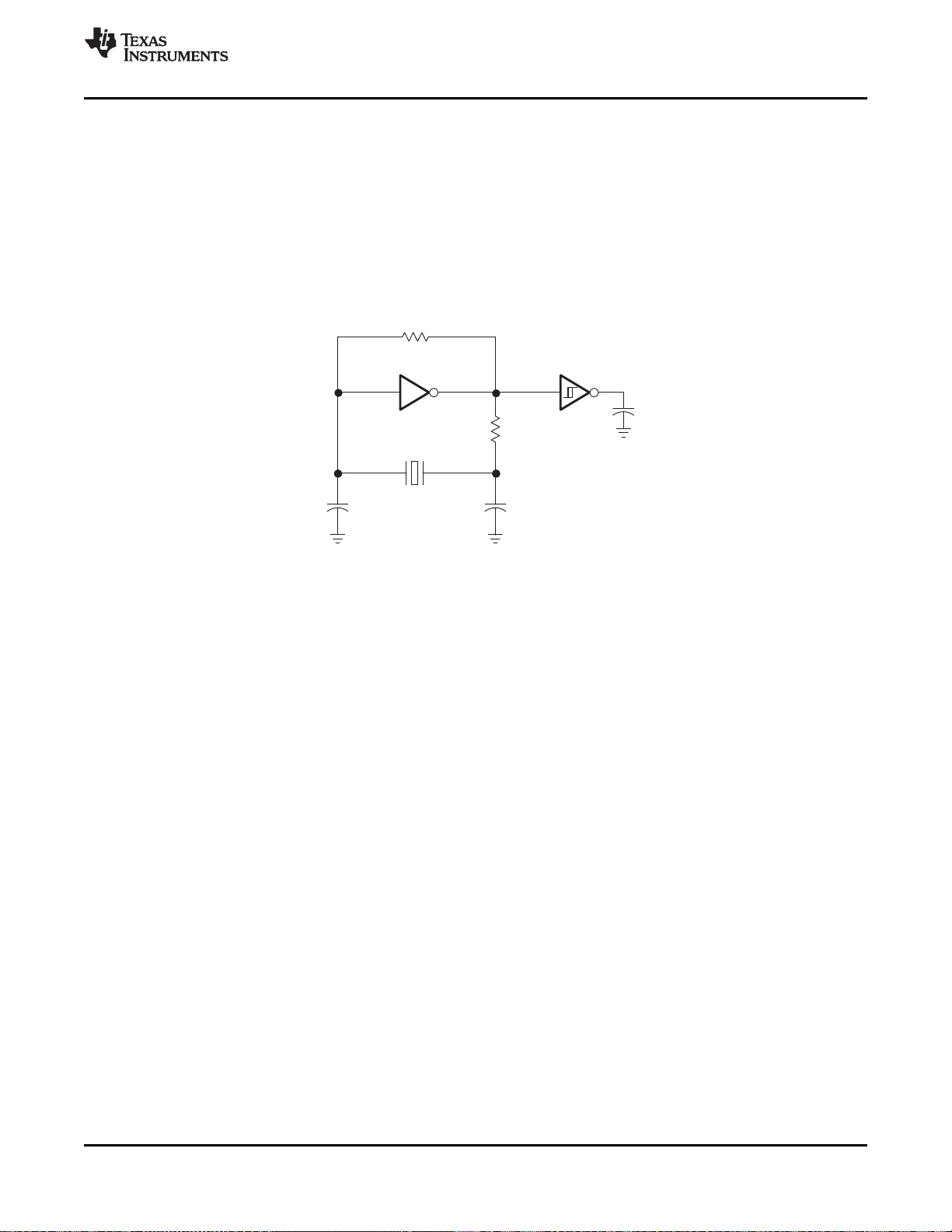
The SN74LVC1G17 device contains one Schmitt trigger buffer and performs the Boolean function Y = A. The
device functions as an independent buffer, but because of Schmitt action, it will have different input threshold
levels for a positive-going (VT+) and negative-going signals.
The DPW package technology is a major breakthrough in IC packaging. Its tiny 0.64 mm square footprint saves
significant board space over other package options while still retaining the traditional manufacturing friendly lead
pitch of 0.5 mm.
This device is fully specified for partial-power-down applications using I
preventing damaging current backflow through the device when it is powered down.
9.2 Functional Block Diagram
9.3 Feature Description
• Wide operating voltage range.
– Operates From 1.65 V to 5.5 V.
• Allows Down voltage translation.
• Inputs accept voltages to 5.5 V.
• I
feature allows voltages on the inputs and outputs, when VCCis 0 V.
off
. The I
off
circuitry disables the outputs,
off
9.4 Device Functional Modes
Table 1. Function Table
INPUT OUTPUT
A Y
H H
L L
10 Submit Documentation Feedback Copyright © 2001–2014, Texas Instruments Incorporated
Product Folder Links: SN74LVC1G17
SN74LVC1G17
R
~2.2 MΩ
F
R
~1 kΩ
S
C
50 pF
C
16 pF
L
C
~32 pF
1
C
~32 pF
2
SN74LVC1G17
www.ti.com
SCES351V –JULY 2001–REVISED APRIL 2014
10 Applications and Implementation
10.1 Application Information
The SN74LVC1G14 is a high drive CMOS device that can be used for a multitude of buffer type functions where
the input is slow or noisy. It can produce 24 mA of drive current at 3.3 V making it Ideal for driving multiple
outputs and good for high speed applications up to 100 MHz. The inputs are 5.5 V tolerant allowing it to translate
down to VCC.
10.2 Typical Application
10.2.1 Design Requirements
This device uses CMOS technology and has balanced output drive. Care should be taken to avoid bus
contention because it can drive currents that would exceed maximum limits. The high drive will also create fast
edges into light loads so routing and load conditions should be considered to prevent ringing.
10.2.2 Detailed Design Procedure
1. Recommended Input Conditions
– Rise time and fall time specs. See (Δt/ΔV) in the Recommended Operating Conditions table.
– Specified high and low levels. See (VIHand VIL) in the Recommended Operating Conditions table.
– Inputs are overvoltage tolerant allowing them to go as high as (VImax) in the Recommended Operating
Conditions table at any valid VCC.
2. Recommend Output Conditions
– Load currents should not exceed (IOmax) per output and should not exceed (continuous current through
VCCor GND) total current for the part. These limits are located in the Absolute Max Ratings table.
– Outputs should not be pulled above VCC.
Copyright © 2001–2014, Texas Instruments Incorporated Submit Documentation Feedback 11
Product Folder Links: SN74LVC1G17
V
CC
Unused Input
Input
Output Output
Input
Unused Input
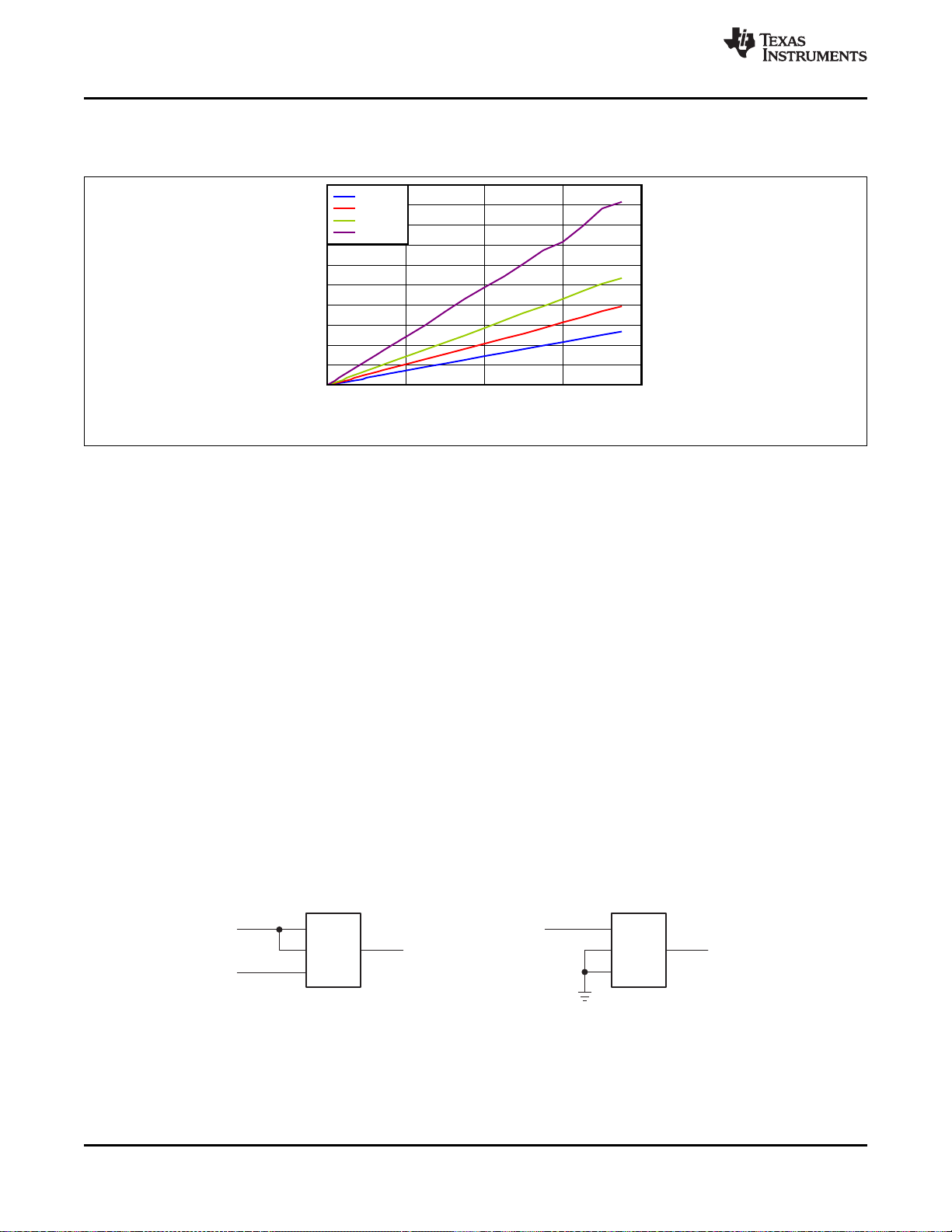
Frequency - MHz
Icc - mA
0 20 40 60 80
0
1
2
3
4
5
6
7
8
9
10
D003
Icc 1.8V
Icc 2.5V
Icc 3.3V
Icc 5V
SN74LVC1G17
SCES351V –JULY 2001–REVISED APRIL 2014
www.ti.com
Typical Application (continued)
10.2.3 Application Curves
Figure 5. ICC vs Frequency
11 Power Supply Recommendations
The power supply can be any voltage between the min and max supply voltage rating located in the
Recommended Operating Conditions table.
Each Vcc pin should have a good bypass capacitor to prevent power disturbance. For devices with a single
supply a 0.1-μF capacitor is recommended and if there are multiple Vcc pins then a 0.01-μF or 0.022-μF
capacitor is recommended for each power pin. It is ok to parallel multiple bypass caps to reject different
frequencies of noise. 0.1-μF and 1-μF capacitors are commonly used in parallel. The bypass capacitor should be
installed as close to the power pin as possible for best results.
12 Layout
12.1 Layout Guidelines
When using multiple bit logic devices inputs should not ever float. In many cases, functions or parts of functions
of digital logic devices are unused, for example, when only two inputs of a triple-input AND gate are used or only
3 of the 4 buffer gates are used. Such input terminals should not be left unconnected because the undefined
voltages at the outside connections result in undefined operational states. Specified below are the rules that must
be observed under all circumstances. All unused inputs of digital logic devices must be connected to a high or
low bias to prevent them from floating. The logic level that should be applied to any particular unused input
depends on the function of the device. Generally they will be tied to Gnd or Vcc whichever make more sense or
is more convenient.
12.2 Layout Example
12 Submit Documentation Feedback Copyright © 2001–2014, Texas Instruments Incorporated
Product Folder Links: SN74LVC1G17

SN74LVC1G17
www.ti.com
SCES351V –JULY 2001–REVISED APRIL 2014
13 Device and Documentation Support
13.1 Trademarks
All trademarks are the property of their respective owners.
13.2 Electrostatic Discharge Caution
These devices have limited built-in ESD protection. The leads should be shorted together or the device placed in conductive foam
during storage or handling to prevent electrostatic damage to the MOS gates.
13.3 Glossary
SLYZ022 — TI Glossary.
This glossary lists and explains terms, acronyms and definitions.
14 Mechanical, Packaging, and Orderable Information
The following pages include mechanical packaging and orderable information. This information is the most
current data available for the designated devices. This data is subject to change without notice and revision of
this document. For browser-based versions of this data sheet, refer to the left-hand navigation.
Copyright © 2001–2014, Texas Instruments Incorporated Submit Documentation Feedback 13
Product Folder Links: SN74LVC1G17

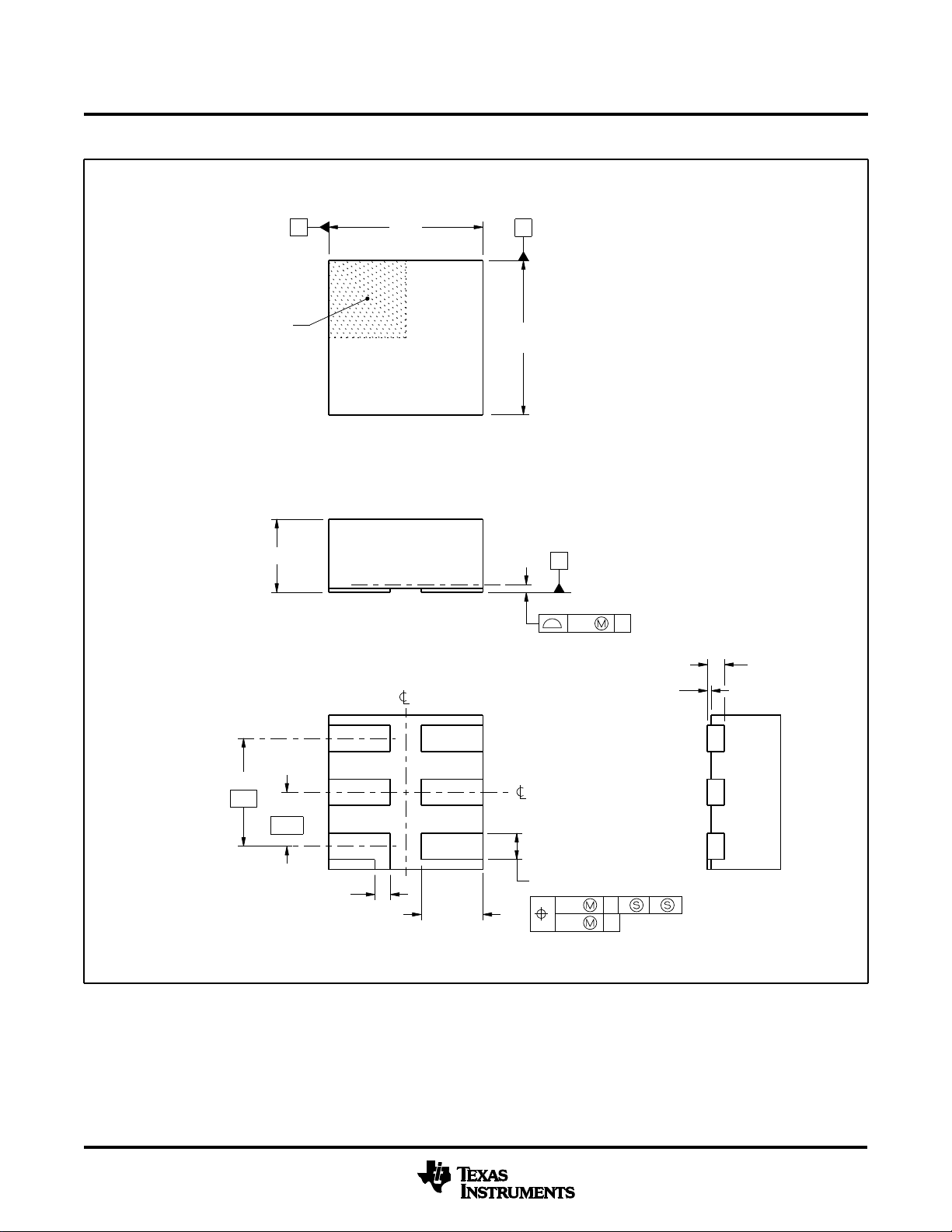
SN74LVC1GXX and SN74AUP1GXXSN74LVC1GXX and SN74AUP1GXX
PACKAGE OUTLINE
PIN 1 INDEX AREA
0.4 MAX
SCALE 12.000
B
0.85
0.75
A
0.85
0.75
C
X2SON - 0.4 mm max heightDPW0005A-C01
PLASTIC SMALL OUTLINE - NO LEAD
SEATING PLANE
NOTE 4
(0.1)
0.05
0.00
NOTE 4
4221849/A 12/2014
THERMAL PAD
2X
0.48
0.27
0.17
2
1
(0.06)
0.25 0.1
0.32
3X
0.23
4
3
5
0.27
4X
0.17
0.1 C A B
0.05 C
NOTES:
1. All linear dimensions are in millimeters. Any dimensions in parenthesis are for reference only. Dimensioning and tolerancing
per ASME Y14.5M.
2. This drawing is subject to change without notice.
3. The package thermal pad must be soldered to the printed circuit board for thermal and mechanical performance.
4. The size and shape of this feature may vary.
www.ti.com

SN74LVC1GXX and SN74AUP1GXX
4X (0.42)
1
(0.78)
SYMM
EXAMPLE BOARD LAYOUT
X2SON - 0.4 mm max heightDPW0005A-C01
PLASTIC SMALL OUTLINE - NO LEAD
( )
0.1
VIA
0.05 MIN
ALL AROUND
TYP
(R ) TYP0.05
4X (0.22)
SYMM
2
( 0.25)
3
4X (0.06)
LAND PATTERN EXAMPLE
SOLDER MASK DEFINED
SCALE:60X
5
4X (0.26)
(0.48)
4
SOLDER MASK
OPENING, TYP
METAL UNDER
SOLDER MASK
TYP
4221849/A 12/2014
NOTES: (continued)
5. This package is designed to be soldered to a thermal pad on the board. For more information, refer to QFN/SON PCB application note
in literature No. SLUA271 (www.ti.com/lit/slua271).
www.ti.com

SN74LVC1GXX and SN74AUP1GXX
EXAMPLE STENCIL DESIGN
X2SON - 0.4 mm max heightDPW0005A-C01
PLASTIC SMALL OUTLINE - NO LEAD
4X (0.22)
(R ) TYP0.05
SYMM
4X (0.42)
1
4X (0.26)
SOLDER MASK
EDGE
2
4X (0.06)
3
SYMM
(0.78)
( 0.24)
(0.21)
TYP
5
(0.48)
4
SOLDER PASTE EXAMPLE
BASED ON 0.1 mm THICK STENCIL
92% PRINTED SOLDER COVERAGE BY AREA
NOTES: (continued)
6. Laser cutting apertures with trapezoidal walls and rounded corners may offer better paste release. IPC-7525 may have alternate
design recommendations.
EXPOSED PAD
SCALE:100X
4221849/A 12/2014
www.ti.com

PACKAGE OPTION ADDENDUM
www.ti.com
PACKAGING INFORMATION
Orderable Device Status
SN74LVC1G17DBVR ACTIVE SOT-23 DBV 5 3000 Green (RoHS
SN74LVC1G17DBVRE4 ACTIVE SOT-23 DBV 5 3000 Green (RoHS
SN74LVC1G17DBVRG4 ACTIVE SOT-23 DBV 5 3000 Green (RoHS
SN74LVC1G17DBVT ACTIVE SOT-23 DBV 5 250 Green (RoHS
SN74LVC1G17DBVTE4 ACTIVE SOT-23 DBV 5 250 Green (RoHS
SN74LVC1G17DBVTG4 ACTIVE SOT-23 DBV 5 250 Green (RoHS
SN74LVC1G17DCKR ACTIVE SC70 DCK 5 3000 Green (RoHS
SN74LVC1G17DCKRE4 ACTIVE SC70 DCK 5 3000 Green (RoHS
SN74LVC1G17DCKRG4 ACTIVE SC70 DCK 5 3000 Green (RoHS
SN74LVC1G17DCKT ACTIVE SC70 DCK 5 250 Green (RoHS
SN74LVC1G17DCKTE4 ACTIVE SC70 DCK 5 250 Green (RoHS
SN74LVC1G17DCKTG4 ACTIVE SC70 DCK 5 250 Green (RoHS
SN74LVC1G17DPWR ACTIVE X2SON DPW 4 3000 Green (RoHS
Package Type Package
(1)
Drawing
Pins Package
Qty
& no Sb/Br)
& no Sb/Br)
& no Sb/Br)
& no Sb/Br)
& no Sb/Br)
& no Sb/Br)
& no Sb/Br)
& no Sb/Br)
& no Sb/Br)
& no Sb/Br)
& no Sb/Br)
& no Sb/Br)
& no Sb/Br)
Eco Plan
(2)
Lead/Ball Finish
(6)
MSL Peak Temp
(3)
Op Temp (°C) Device Marking
(4/5)
CU NIPDAU Level-1-260C-UNLIM -40 to 125 (C175 ~ C17F ~
C17K ~ C17R)
(C17H ~ C17P ~
C17S)
CU NIPDAU Level-1-260C-UNLIM -40 to 125 C17F
CU NIPDAU Level-1-260C-UNLIM -40 to 125 C17F
CU NIPDAU Level-1-260C-UNLIM -40 to 125 (C175 ~ C17F ~
C17K ~ C17R)
(C17H ~ C17P ~
C17S)
CU NIPDAU Level-1-260C-UNLIM -40 to 125 C17F
CU NIPDAU Level-1-260C-UNLIM -40 to 125 C17F
CU NIPDAU Level-1-260C-UNLIM -40 to 125 (C75 ~ C7F ~ C7K ~
C7R ~ C7T)
(C7H ~ C7P ~ C7S)
CU NIPDAU Level-1-260C-UNLIM -40 to 125 (C75 ~ C7F ~ C7K ~
C7R ~ C7T)
(C7H ~ C7P ~ C7S)
CU NIPDAU Level-1-260C-UNLIM -40 to 125 (C75 ~ C7F ~ C7K ~
C7R ~ C7T)
(C7H ~ C7P ~ C7S)
CU NIPDAU Level-1-260C-UNLIM -40 to 125 (C75 ~ C7F ~ C7K ~
C7R ~ C7T)
(C7H ~ C7P ~ C7S)
CU NIPDAU Level-1-260C-UNLIM -40 to 125 (C75 ~ C7F ~ C7K ~
C7R ~ C7T)
(C7H ~ C7P ~ C7S)
CU NIPDAU Level-1-260C-UNLIM -40 to 125 (C75 ~ C7F ~ C7K ~
C7R ~ C7T)
(C7H ~ C7P ~ C7S)
CU NIPDAU Level-1-260C-UNLIM -40 to 125 S4
3-Nov-2015
Samples
Addendum-Page 1

PACKAGE OPTION ADDENDUM
www.ti.com
Orderable Device Status
SN74LVC1G17DRLR ACTIVE SOT DRL 5 4000 Green (RoHS
SN74LVC1G17DRLRG4 ACTIVE SOT DRL 5 4000 Green (RoHS
SN74LVC1G17DRY2 PREVIEW SON DRY 6 5000 Green (RoHS
SN74LVC1G17DRYR ACTIVE SON DRY 6 5000 Green (RoHS
SN74LVC1G17DSF2 PREVIEW SON DSF 6 5000 Green (RoHS
SN74LVC1G17DSFR ACTIVE SON DSF 6 5000 Green (RoHS
SN74LVC1G17YZPR ACTIVE DSBGA YZP 5 3000 Green (RoHS
SN74LVC1G17YZVR ACTIVE DSBGA YZV 4 3000 Green (RoHS
(1)
The marketing status values are defined as follows:
ACTIVE: Product device recommended for new designs.
LIFEBUY: TI has announced that the device will be discontinued, and a lifetime-buy period is in effect.
NRND: Not recommended for new designs. Device is in production to support existing customers, but TI does not recommend using this part in a new design.
PREVIEW: Device has been announced but is not in production. Samples may or may not be available.
OBSOLETE: TI has discontinued the production of the device.
Package Type Package
(1)
Drawing
Pins Package
Qty
Eco Plan
(2)
& no Sb/Br)
& no Sb/Br)
& no Sb/Br)
& no Sb/Br)
& no Sb/Br)
& no Sb/Br)
& no Sb/Br)
& no Sb/Br)
Lead/Ball Finish
(6)
CU NIPDAU Level-1-260C-UNLIM -40 to 125 (C77 ~ C7R)
CU NIPDAU Level-1-260C-UNLIM -40 to 125 (C77 ~ C7R)
CU NIPDAU Level-1-260C-UNLIM -40 to 125 C7
CU NIPDAU Level-1-260C-UNLIM -40 to 125 C7
CU NIPDAU |
CU NIPDAUAG
CU NIPDAU |
CU NIPDAUAG
SNAGCU Level-1-260C-UNLIM -40 to 85 (C77 ~ C7N)
SNAGCU Level-1-260C-UNLIM -40 to 85 C7
MSL Peak Temp
(3)
Level-1-260C-UNLIM -40 to 125 C7
Level-1-260C-UNLIM -40 to 125 C7
Op Temp (°C) Device Marking
(7 ~ N)
(4/5)
(2)
Eco Plan - The planned eco-friendly classification: Pb-Free (RoHS), Pb-Free (RoHS Exempt), or Green (RoHS & no Sb/Br) - please check http://www.ti.com/productcontent for the latest availability
information and additional product content details.
TBD: The Pb-Free/Green conversion plan has not been defined.
Pb-Free (RoHS): TI's terms "Lead-Free" or "Pb-Free" mean semiconductor products that are compatible with the current RoHS requirements for all 6 substances, including the requirement that
lead not exceed 0.1% by weight in homogeneous materials. Where designed to be soldered at high temperatures, TI Pb-Free products are suitable for use in specified lead-free processes.
Pb-Free (RoHS Exempt): This component has a RoHS exemption for either 1) lead-based flip-chip solder bumps used between the die and package, or 2) lead-based die adhesive used between
the die and leadframe. The component is otherwise considered Pb-Free (RoHS compatible) as defined above.
Green (RoHS & no Sb/Br): TI defines "Green" to mean Pb-Free (RoHS compatible), and free of Bromine (Br) and Antimony (Sb) based flame retardants (Br or Sb do not exceed 0.1% by weight
in homogeneous material)
(3)
MSL, Peak Temp. - The Moisture Sensitivity Level rating according to the JEDEC industry standard classifications, and peak solder temperature.
(4)
There may be additional marking, which relates to the logo, the lot trace code information, or the environmental category on the device.
3-Nov-2015
Samples
Addendum-Page 2
PACKAGE OPTION ADDENDUM
www.ti.com
(5)
Multiple Device Markings will be inside parentheses. Only one Device Marking contained in parentheses and separated by a "~" will appear on a device. If a line is indented then it is a continuation
of the previous line and the two combined represent the entire Device Marking for that device.
(6)
Lead/Ball Finish - Orderable Devices may have multiple material finish options. Finish options are separated by a vertical ruled line. Lead/Ball Finish values may wrap to two lines if the finish
value exceeds the maximum column width.
Important Information and Disclaimer:The information provided on this page represents TI's knowledge and belief as of the date that it is provided. TI bases its knowledge and belief on information
provided by third parties, and makes no representation or warranty as to the accuracy of such information. Efforts are underway to better integrate information from third parties. TI has taken and
continues to take reasonable steps to provide representative and accurate information but may not have conducted destructive testing or chemical analysis on incoming materials and chemicals.
TI and TI suppliers consider certain information to be proprietary, and thus CAS numbers and other limited information may not be available for release.
In no event shall TI's liability arising out of such information exceed the total purchase price of the TI part(s) at issue in this document sold by TI to Customer on an annual basis.
OTHER QUALIFIED VERSIONS OF SN74LVC1G17 :
Automotive: SN74LVC1G17-Q1
•
Enhanced Product: SN74LVC1G17-EP
•
NOTE: Qualified Version Definitions:
Automotive - Q100 devices qualified for high-reliability automotive applications targeting zero defects
•
3-Nov-2015
Enhanced Product - Supports Defense, Aerospace and Medical Applications
•
Addendum-Page 3

PACKAGE MATERIALS INFORMATION
www.ti.com 13-Nov-2015
TAPE AND REEL INFORMATION
*All dimensions are nominal
Device Package
Type
SN74LVC1G17DBVR SOT-23 DBV 5 3000 180.0 9.2 3.17 3.23 1.37 4.0 8.0 Q3
SN74LVC1G17DBVR SOT-23 DBV 5 3000 180.0 8.4 3.23 3.17 1.37 4.0 8.0 Q3
SN74LVC1G17DBVRG4 SOT-23 DBV 5 3000 178.0 9.0 3.23 3.17 1.37 4.0 8.0 Q3
SN74LVC1G17DBVTG4 SOT-23 DBV 5 250 178.0 9.0 3.23 3.17 1.37 4.0 8.0 Q3
SN74LVC1G17DCKR SC70 DCK 5 3000 178.0 9.0 2.4 2.5 1.2 4.0 8.0 Q3
SN74LVC1G17DCKR SC70 DCK 5 3000 178.0 9.2 2.4 2.4 1.22 4.0 8.0 Q3
SN74LVC1G17DCKT SC70 DCK 5 250 178.0 9.0 2.4 2.5 1.2 4.0 8.0 Q3
SN74LVC1G17DCKT SC70 DCK 5 250 180.0 9.2 2.3 2.55 1.2 4.0 8.0 Q3
SN74LVC1G17DCKT SC70 DCK 5 250 178.0 9.2 2.4 2.4 1.22 4.0 8.0 Q3
SN74LVC1G17DRLR SOT DRL 5 4000 180.0 8.4 1.98 1.78 0.69 4.0 8.0 Q3
SN74LVC1G17DRYR SON DRY 6 5000 179.0 8.4 1.2 1.65 0.7 4.0 8.0 Q1
SN74LVC1G17DSFR SON DSF 6 5000 180.0 9.5 1.16 1.16 0.5 4.0 8.0 Q2
SN74LVC1G17YZPR DSBGA YZP 5 3000 178.0 9.2 1.02 1.52 0.63 4.0 8.0 Q1
SN74LVC1G17YZVR DSBGA YZV 4 3000 178.0 9.2 1.0 1.0 0.63 4.0 8.0 Q1
Package
Drawing
Pins SPQ Reel
Diameter
(mm)
Reel
Width
W1 (mm)
A0
(mm)B0(mm)K0(mm)P1(mm)W(mm)
Quadrant
Pin1
Pack Materials-Page 1

PACKAGE MATERIALS INFORMATION
www.ti.com 13-Nov-2015
*All dimensions are nominal
Device Package Type Package Drawing Pins SPQ Length (mm) Width (mm) Height (mm)
SN74LVC1G17DBVR SOT-23 DBV 5 3000 205.0 200.0 33.0
SN74LVC1G17DBVR SOT-23 DBV 5 3000 202.0 201.0 28.0
SN74LVC1G17DBVRG4 SOT-23 DBV 5 3000 180.0 180.0 18.0
SN74LVC1G17DBVTG4 SOT-23 DBV 5 250 180.0 180.0 18.0
SN74LVC1G17DCKR SC70 DCK 5 3000 180.0 180.0 18.0
SN74LVC1G17DCKR SC70 DCK 5 3000 180.0 180.0 18.0
SN74LVC1G17DCKT SC70 DCK 5 250 180.0 180.0 18.0
SN74LVC1G17DCKT SC70 DCK 5 250 205.0 200.0 33.0
SN74LVC1G17DCKT SC70 DCK 5 250 180.0 180.0 18.0
SN74LVC1G17DRLR SOT DRL 5 4000 202.0 201.0 28.0
SN74LVC1G17DRYR SON DRY 6 5000 203.0 203.0 35.0
SN74LVC1G17DSFR SON DSF 6 5000 184.0 184.0 19.0
SN74LVC1G17YZPR DSBGA YZP 5 3000 220.0 220.0 35.0
SN74LVC1G17YZVR DSBGA YZV 4 3000 220.0 220.0 35.0
Pack Materials-Page 2


MECHANICAL DATA
DSF (S-PX2SON-N6)
PIN 1 INDEX AREA
0.4 MAX
PLASTIC SMALL OUTLINE NO-LEAD
A
1.05
0.95
B
1.05
0.95
C
SEATING PLANE
0.05 C
(0.11) TYP
2X
0.7
4X
0.35
3
1
(0.1)
PIN 1 ID
SYMM
6X
0.45
0.35
4
6
SYMM
0.22
6X
0.12
0.07 C A B
0.05 C
0.05
0.00
4208186/F 10/2014
NOTES:
1. All linear dimensions are in millimeters. Any dimensions in parenthesis are for reference only. Dimensioning and tolerancing
per ASME Y14.5M.
2. This drawing is subject to change without notice.
3. Reference JEDEC registration MO-287, variation X2AAF.
www.ti.com


D: Max =
1.418 mm, Min =
1.357 mm
E: Max =
0.918 mm, Min =
0.857 mm


D: Max =
0.918 mm, Min =
0.858 mm
E: Max =
0.918 mm, Min =
0.858 mm
D: Max =
0.918 mm, Min =
0.858 mm
E: Max =
0.918 mm, Min =
0.858 mm

IMPORTANT NOTICE
Texas Instruments Incorporated and its subsidiaries (TI) reserve the right to make corrections, enhancements, improvements and other
changes to its semiconductor products and services per JESD46, latest issue, and to discontinue any product or service per JESD48, latest
issue. Buyers should obtain the latest relevant information before placing orders and should verify that such information is current and
complete. All semiconductor products (also referred to herein as “components”) are sold subject to TI’s terms and conditions of sale
supplied at the time of order acknowledgment.
TI warrants performance of its components to the specifications applicable at the time of sale, in accordance with the warranty in TI’s terms
and conditions of sale of semiconductor products. Testing and other quality control techniques are used to the extent TI deems necessary
to support this warranty. Except where mandated by applicable law, testing of all parameters of each component is not necessarily
performed.
TI assumes no liability for applications assistance or the design of Buyers’ products. Buyers are responsible for their products and
applications using TI components. To minimize the risks associated with Buyers’ products and applications, Buyers should provide
adequate design and operating safeguards.
TI does not warrant or represent that any license, either express or implied, is granted under any patent right, copyright, mask work right, or
other intellectual property right relating to any combination, machine, or process in which TI components or services are used. Information
published by TI regarding third-party products or services does not constitute a license to use such products or services or a warranty or
endorsement thereof. Use of such information may require a license from a third party under the patents or other intellectual property of the
third party, or a license from TI under the patents or other intellectual property of TI.
Reproduction of significant portions of TI information in TI data books or data sheets is permissible only if reproduction is without alteration
and is accompanied by all associated warranties, conditions, limitations, and notices. TI is not responsible or liable for such altered
documentation. Information of third parties may be subject to additional restrictions.
Resale of TI components or services with statements different from or beyond the parameters stated by TI for that component or service
voids all express and any implied warranties for the associated TI component or service and is an unfair and deceptive business practice.
TI is not responsible or liable for any such statements.
Buyer acknowledges and agrees that it is solely responsible for compliance with all legal, regulatory and safety-related requirements
concerning its products, and any use of TI components in its applications, notwithstanding any applications-related information or support
that may be provided by TI. Buyer represents and agrees that it has all the necessary expertise to create and implement safeguards which
anticipate dangerous consequences of failures, monitor failures and their consequences, lessen the likelihood of failures that might cause
harm and take appropriate remedial actions. Buyer will fully indemnify TI and its representatives against any damages arising out of the use
of any TI components in safety-critical applications.
In some cases, TI components may be promoted specifically to facilitate safety-related applications. With such components, TI’s goal is to
help enable customers to design and create their own end-product solutions that meet applicable functional safety standards and
requirements. Nonetheless, such components are subject to these terms.
No TI components are authorized for use in FDA Class III (or similar life-critical medical equipment) unless authorized officers of the parties
have executed a special agreement specifically governing such use.
Only those TI components which TI has specifically designated as military grade or “enhanced plastic” are designed and intended for use in
military/aerospace applications or environments. Buyer acknowledges and agrees that any military or aerospace use of TI components
which have not been so designated is solely at the Buyer's risk, and that Buyer is solely responsible for compliance with all legal and
regulatory requirements in connection with such use.
TI has specifically designated certain components as meeting ISO/TS16949 requirements, mainly for automotive use. In any case of use of
non-designated products, TI will not be responsible for any failure to meet ISO/TS16949.
Products Applications
Audio www.ti.com/audio Automotive and Transportation www.ti.com/automotive
Amplifiers amplifier.ti.com Communications and Telecom www.ti.com/communications
Data Converters dataconverter.ti.com Computers and Peripherals www.ti.com/computers
DLP® Products www.dlp.com Consumer Electronics www.ti.com/consumer-apps
DSP dsp.ti.com Energy and Lighting www.ti.com/energy
Clocks and Timers www.ti.com/clocks Industrial www.ti.com/industrial
Interface interface.ti.com Medical www.ti.com/medical
Logic logic.ti.com Security www.ti.com/security
Power Mgmt power.ti.com Space, Avionics and Defense www.ti.com/space-avionics-defense
Microcontrollers microcontroller.ti.com Video and Imaging www.ti.com/video
RFID www.ti-rfid.com
OMAP Applications Processors www.ti.com/omap TI E2E Community e2e.ti.com
Wireless Connectivity www.ti.com/wirelessconnectivity
Mailing Address: Texas Instruments, Post Office Box 655303, Dallas, Texas 75265
Copyright © 2015, Texas Instruments Incorporated

 Loading...