

Page 1
Reel of 3000
SOT (SOT-23)
DBV
C25
SOT (SC-70)
DCK
CM
SN74LVC1G125
SINGLE BUS BUFFER GATE
WITH 3-STATE OUTPUT
SCES223J – APRIL 1999 – REVISED MA Y 2003
D
Available in the Texas Instruments
NanoStar and NanoFree Packages
D
Supports 5-V VCC Operation
D
Inputs Accept Voltages to 5.5 V
D
Max tpd of 3.7 ns at 3.3 V
D
Low Power Consumption, 10-µA Max I
D
±24-mA Output Drive at 3.3 V
D
I
Supports Partial-Power-Down Mode
off
Operation
D
Latch-Up Performance Exceeds 100 mA
Per JESD 78, Class II
D
ESD Protection Exceeds JESD 22
CC
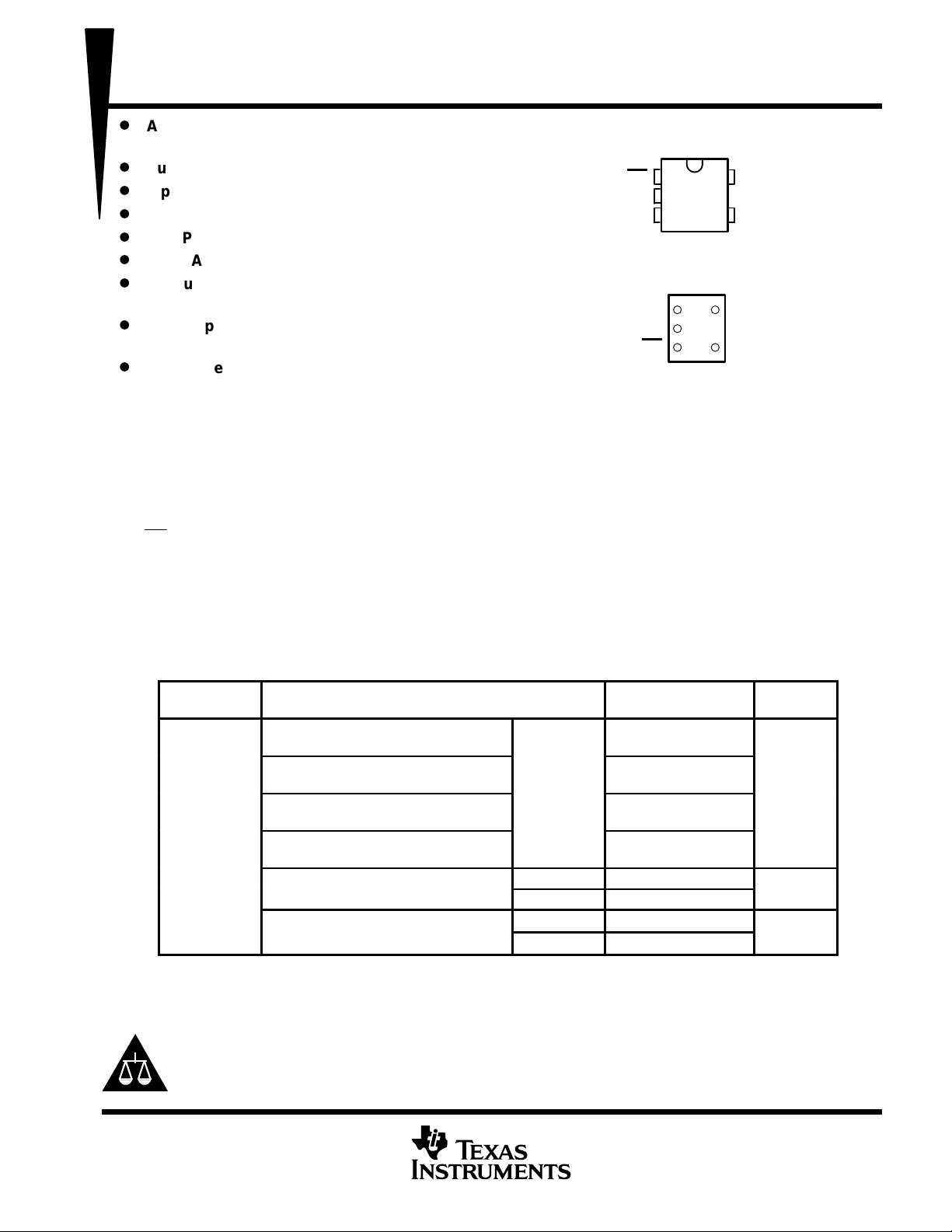
DBV OR DCK PACKAGE
(TOP VIEW)
1
OE
2
A
GND
YEA, YEP, YZA OR YZP PACKAGE
3
(BOTTOM VIEW)
GND
A
OE
3
2
145
5
V
CC
4
Y
Y
V
CC
– 2000-V Human-Body Model (A114-A)
– 200-V Machine Model (A115-A)
– 1000-V Charged-Device Model (C101)
description/ordering information
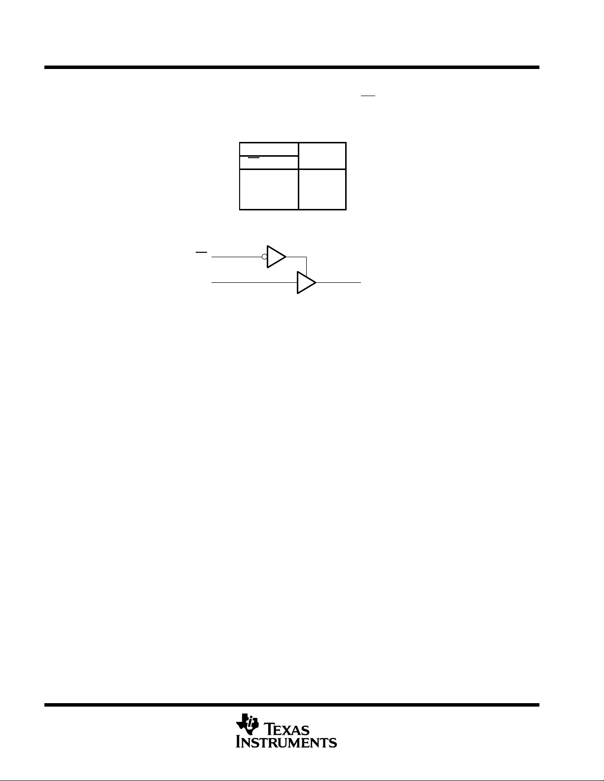
This bus buffer gate is designed for 1.65-V to 5.5-V VCC operation.
The SN74L VC1G125 is a single line driver with a 3-state output. The output is disabled when the output-enable
) input is high.
(OE
NanoStarand NanoFreepackage technology is a major breakthrough in IC packaging concepts, using the
die as the package.
This device is fully specified for partial-power-down applications using I
off
. The I
circuitry disables the outputs,
off
preventing damaging current backflow through the device when it is powered down.
ORDERING INFORMA TION
T
A
NanoStar – WCSP (DSBGA)
0.17-mm Small Bump – YEA
NanoFree – WCSP (DSBGA)
0.17-mm Small Bump – YZA (Pb-free)
NanoStar – WCSP (DSBGA)
0.23-mm Large Bump – YEP
–40°C to 85°C
†
Package drawings, standard packing quantities, thermal data, symbolization, and PCB design guidelines are available at
www.ti.com/sc/package.
‡
DBV/DCK: The actual top-side marking has one additional character that designates the assembly/test site.
YEA/YZA, YEP/YZP: The actual top-side marking has three preceding characters to denote year, month, and sequence code,
and one following character to designate the assembly/test site.
Please be aware that an important notice concerning availability, standard warranty, and use in critical applications of
Texas Instruments semiconductor products and disclaimers thereto appears at the end of this data sheet.
NanoFree – WCSP (DSBGA)
0.23-mm Large Bump – YZP (Pb-free)
–
–
PACKAGE
†
Reel of 3000 SN74LVC1G125DBVR
Reel of 250 SN74LVC1G125DBVT
Reel of 3000 SN74LVC1G125DCKR
Reel of 250 SN74LVC1G125DCKT
ORDERABLE
PART NUMBER
SN74LVC1G125YEAR
SN74LVC1G125YZAR
SN74LVC1G125YEPR
SN74LVC1G125YZPR
TOP-SIDE
MARKING
_ _ _CM_
‡
_
_
NanoStar and NanoFree are trademarks of Texas Instruments.
PRODUCTION DATA information is current as of publication date.
Products conform to specifications per the terms of Texas Instruments
standard warranty. Production processing does not necessarily include
testing of all parameters.
POST OFFICE BOX 655303 • DALLAS, TEXAS 75265
Copyright 2003, Texas Instruments Incorporated
1
Page 2
SN74LVC1G125
SINGLE BUS BUFFER GATE
WITH 3-STATE OUTPUT
SCES223J – APRIL 1999 – REVISED MAY 2003
description/ordering information (continued)
T o ensure the high-impedance state during power up or power down, OE should be tied to VCC through a pullup
resistor; the minimum value of the resistor is determined by the current-sinking capability of the driver.
FUNCTION TABLE
logic diagram (positive logic)
INPUTS
OE A
L H H
L LL
H X Z
1
OE
24
AY
OUTPUT
Y
absolute maximum ratings over operating free-air temperature range (unless otherwise noted)
Supply voltage range, V
Input voltage range, V
Voltage range applied to any output in the high-impedance or power-off state, V
(see Note 1) –0.5 V to 6.5 V. . . . . . . . . . . . . . . . . . . . . . . . . . . . . . . . . . . . . . . . . . . . . . . . . . . . . . . . . . . . . . . . . . .
Voltage range applied to any output in the high or low state, V
(see Notes 1 and 2) –0.5 V to V
Input clamp current, I
Output clamp current, I
Continuous output current, I
Continuous current through V
Package thermal impedance, θ
Storage temperature range, T
†
Stresses beyond those listed under “absolute maximum ratings” may cause permanent damage to the device. These are stress ratings only, and
functional operation of the device at these or any other conditions beyond those indicated under “recommended operating conditions” is not implied.
Exposure to absolute-maximum-rated conditions for extended periods may affect device reliability.
NOTES: 1. The input negative-voltage and output voltage ratings may be exceeded if the input and output current ratings are observed.
2. The value of VCC is provided in the recommended operating conditions table.
3. The package thermal impedance is calculated in accordance with JESD 51-7.
–0.5 V to 6.5 V. . . . . . . . . . . . . . . . . . . . . . . . . . . . . . . . . . . . . . . . . . . . . . . . . . . . . . . . .
CC
(see Note 1) –0.5 V to 6.5 V. . . . . . . . . . . . . . . . . . . . . . . . . . . . . . . . . . . . . . . . . . . . . . . . .
I
O
O
(VI < 0) –50 mA. . . . . . . . . . . . . . . . . . . . . . . . . . . . . . . . . . . . . . . . . . . . . . . . . . . . . . . . . . .
IK
(VO < 0) –50 mA. . . . . . . . . . . . . . . . . . . . . . . . . . . . . . . . . . . . . . . . . . . . . . . . . . . . . . . .
OK
±50 mA. . . . . . . . . . . . . . . . . . . . . . . . . . . . . . . . . . . . . . . . . . . . . . . . . . . . . . . . . . . . .
O
or GND ±100 mA. . . . . . . . . . . . . . . . . . . . . . . . . . . . . . . . . . . . . . . . . . . . . . . . . .
CC
(see Note 3): DBV package 206°C/W. . . . . . . . . . . . . . . . . . . . . . . . . . . . . . .
JA
DCK package 252°C/W. . . . . . . . . . . . . . . . . . . . . . . . . . . . . . .
YEA/YZA package 154°C/W. . . . . . . . . . . . . . . . . . . . . . . . . . .
YEP/YZP package 132°C/W. . . . . . . . . . . . . . . . . . . . . . . . . . .
–65°C to 150°C. . . . . . . . . . . . . . . . . . . . . . . . . . . . . . . . . . . . . . . . . . . . . . . . . . .
stg
CC
+ 0.5 V. . . . . . . . . . . . . . . . . . . . . . . . . . . . . . . . . . . . . . . . . . . . . . . . . . . . . . .
†
2
POST OFFICE BOX 655303 • DALLAS, TEXAS 75265
Page 3
VCCSuppl
oltage
V
VIHHigh-level input voltage
V
VILLow-level input voltage
V
V
3 V
V
3 V
SN74LVC1G125
SINGLE BUS BUFFER GATE
WITH 3-STATE OUTPUT
SCES223J – APRIL 1999 – REVISED MAY 2003
recommended operating conditions (see Note 4)
MIN MAX UNIT
pp
y v
p
p
V
Input voltage 0 5.5 V
I
V
Output voltage 0 V
O
I
High-level output current
OH
I
Low-level output current
OL
∆t/∆v Input transition rise or fall rate
T
Operating free-air temperature –40 85 °C
A
NOTE 4: All unused inputs of the device must be held at VCC or GND to ensure proper device operation. Refer to the TI application report,
Implications of Slow or Floating CMOS Inputs, literature number SCBA004.
Operating 1.65 5.5
Data retention only 1.5
VCC = 1.65 V to 1.95 V 0.65 × V
VCC = 2.3 V to 2.7 V 1.7
VCC = 3 V to 3.6 V 2
VCC = 4.5 V to 5.5 V 0.7 × V
VCC = 1.65 V to 1.95 V 0.35 × V
VCC = 2.3 V to 2.7 V 0.7
VCC = 3 V to 3.6 V 0.8
VCC = 4.5 V to 5.5 V 0.3 × V
VCC = 1.65 V –4
VCC = 2.3 V –8
=
CC
VCC = 4.5 V –32
VCC = 1.65 V 4
VCC = 2.3 V 8
=
CC
VCC = 4.5 V 32
VCC = 1.8 V ± 0.15 V, 2.5 V ± 0.2 V 20
VCC = 3.3 V ± 0.3 V
VCC = 5 V ± 0.5 V 5
CC
CC
CC
–16
–24
16
24
10
CC
CC
V
mA
mA
ns/V
POST OFFICE BOX 655303 • DALLAS, TEXAS 75265
3
Page 4
SN74LVC1G125
PARAMETER
TEST CONDITIONS
VCCMIN
TYP
†
MAX
UNIT
3 V
3 V
(INPUT)
(OUTPUT)
(INPUT)
(OUTPUT)
PARAMETER
UNIT
C
d
f
pF
SINGLE BUS BUFFER GATE
WITH 3-STATE OUTPUT
SCES223J – APRIL 1999 – REVISED MAY 2003
electrical characteristics over recommended operating free-air temperature range (unless
otherwise noted)
IOH = –100 mA 1.65 V to 5.5 V VCC–0.1
IOH = –4 mA 1.65 V 1.2
V
OH
V
OL
I
A or OE inputs
I
I
off
I
OZ
I
CC
∆I
CC
C
i
†
All typical values are at VCC = 3.3 V, TA = 25°C.
IOH = –8 mA 2.3 V 1.9
IOH = –16 mA
IOH = –24 mA
IOH = –32 mA
IOL = 100 mA 1.65 V to 5.5 V 0.1
IOL = 4 mA 1.65 V 0.45
IOL = 8 mA 2.3 V 0.3
IOL = 16 mA
IOL = 24 mA
IOL = 32 mA
VI = 5.5 V or GND 0 to 5.5 V ±5
VI or VO = 5.5 V 0 ±10
VO = 0 to 5.5 V 3.6 V 10
VI = 5.5 V or GND, IO = 0 1.65 V to 5.5 V 10
One input at VCC – 0.6 V, Other inputs at VCC or GND 3 V to 5.5 V 500
VI = VCC or GND 3.3 V 4 pF
4.5 V 3.8
4.5 V 0.55
2.4
2.3
0.4
0.55
m
m
m
m
m
V
V
A
A
A
A
A
switching characteristics over recommended operating free-air temperature range, CL = 15 pF
(unless otherwise noted) (see Figure 1)
PARAMETER
t
pd
FROM
A
TO
VCC = 1.8 V
± 0.15 V
MIN MAX MIN MAX MIN MAX MIN MAX
Y
1.9 6.9 0.7 4.6 0.6 3.7 0.5 3.4 ns
VCC = 2.5 V
± 0.2 V
VCC = 3.3 V
± 0.3 V
VCC = 5 V
± 0.5 V
UNIT
switching characteristics over recommended operating free-air temperature range, CL = 30 pF or
50 pF (unless otherwise noted) (see Figure 2)
PARAMETER
t
pd
t
en
t
dis
FROM
A
OE
OE
operating characteristics, T
Power dissipation
p
capacitance
Outputs enabled
Outputs disabled
= 25°C
A
TO
Y
Y
Y
TEST
CONDITIONS
= 10 MHz
VCC = 1.8 V
± 0.15 V
MIN MAX MIN MAX MIN MAX MIN MAX
2.8 8 1.2 5.5 1 4.5 1 4 ns
3.3 9.4 1.5 6.6 1 5.3 1 5 ns
1.3 9.2 1 5 1 5 1 4.2 ns
VCC = 1.8 V VCC = 2.5 V VCC = 3.3 V VCC = 5 V
TYP TYP TYP TYP
18 18 19 21
VCC = 2.5 V
± 0.2 V
2 2 2 4
VCC = 3.3 V
± 0.3 V
VCC = 5 V
± 0.5 V
UNIT
p
4
POST OFFICE BOX 655303 • DALLAS, TEXAS 75265
Page 5

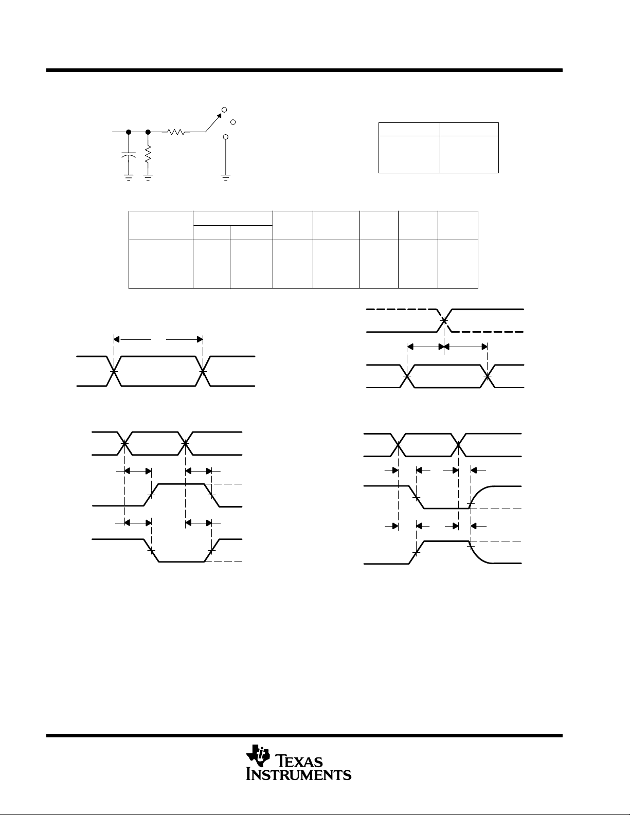
From Output
Under Test
(see Note A)
C
L
R
L
R
L
LOAD CIRCUIT
SINGLE BUS BUFFER GATE
SCES223J – APRIL 1999 – REVISED MAY 2003
PARAMETER MEASUREMENT INFORMATION
V
S1
LOAD
Open
GND
TEST S1
t
PLH/tPHL
t
PLZ/tPZL
t
PHZ/tPZH
SN74LVC1G125
WITH 3-STATE OUTPUT
Open
V
LOAD
GND
V
CC
1.8 V ± 0.15 V
2.5 V ± 0.2 V
3.3 V ± 0.3 V
5 V ± 0.5 V
t
w
Input
Input
Output
Output
INVERTING AND NONINVERTING OUTPUTS
NOTES: A. CL includes probe and jig capacitance.
B. Waveform 1 is for an output with internal conditions such that the output is low except when disabled by the output control.
C. All input pulses are supplied by generators having the following characteristics: PRR ≤ 10 MHz, ZO = 50 Ω.
D. The outputs are measured one at a time with one transition per measurement.
E. t
F. t
G. t
H. All parameters and waveforms are not applicable to all devices.
V
M
VOLTAGE WAVEFORMS
PULSE DURATION
V
M
t
PLH
V
M
t
PHL
V
M
VOLTAGE WAVEFORMS
PROPAGATION DELAY TIMES
Waveform 2 is for an output with internal conditions such that the output is high except when disabled by the output control.
PLZ
PZL
PLH
and t
and t
and t
are the same as t
PHZ
are the same as ten.
PZH
are the same as tpd.
PHL
INPUTS
V
I
V
CC
V
CC
3 V
V
CC
V
M
V
M
t
PHL
V
M
t
PLH
V
M
.
dis
tr/t
f
≤2 ns
≤2 ns
≤2.5 ns
≤2.5 ns
V
I
0 V
V
OH
V
OL
V
OH
V
OL
V
0 V
I
V
M
VCC/2
VCC/2
1.5 V
VCC/2
V
LOAD
2 × V
CC
2 × V
CC
6 V
2 × V
CC
Timing Input
Data Input
Output
Control
Output
Waveform 1
S1 at V
LOAD
(see Note B)
Output
Waveform 2
S1 at GND
(see Note B)
su
V
V
V
∆
0.15 V
0.15 V
0.3 V
0.3 V
V
M
t
h
V
M
M
M
VOL + V
VOH – V
C
L
15 pF
15 pF
15 pF
15 pF
t
PZL
t
PZH
ENABLE AND DISABLE TIMES
LOW- AND HIGH-LEVEL ENABLING
R
L
1 MΩ
1 MΩ
1 MΩ
1 MΩ
t
V
M
VOLTAGE WAVEFORMS
SETUP AND HOLD TIMES
V
M
VOLTAGE WAVEFORMS
t
PLZ
t
PHZ
V
I
0 V
V
V
M
I
0 V
V
I
0 V
V
/2
LOAD
∆
V
OL
V
OH
∆
≈0 V
Figure 1. Load Circuit and Voltage Waveforms
POST OFFICE BOX 655303 • DALLAS, TEXAS 75265
5
Page 6
SN74LVC1G125
SINGLE BUS BUFFER GATE
WITH 3-STATE OUTPUT
SCES223J – APRIL 1999 – REVISED MAY 2003
PARAMETER MEASUREMENT INFORMATION
R
From Output
Under Test
(see Note A)
C
L
LOAD CIRCUIT
L
R
L
S1
V
LOAD
GND
Open
TEST S1
t
PLH/tPHL
t
PLZ/tPZL
t
PHZ/tPZH
Open
V
LOAD
GND
V
CC
1.8 V ± 0.15 V
2.5 V ± 0.2 V
3.3 V ± 0.3 V
5 V ± 0.5 V
t
w
Input
Input
Output
Output
INVERTING AND NONINVERTING OUTPUTS
NOTES: A. CL includes probe and jig capacitance.
B. Waveform 1 is for an output with internal conditions such that the output is low except when disabled by the output control.
C. All input pulses are supplied by generators having the following characteristics: PRR ≤ 10 MHz, ZO = 50 Ω.
D. The outputs are measured one at a time with one transition per measurement.
E. t
F. t
G. t
H. All parameters and waveforms are not applicable to all devices.
V
M
VOLTAGE WAVEFORMS
PULSE DURATION
V
M
t
PLH
V
M
t
PHL
V
M
VOLTAGE WAVEFORMS
PROPAGATION DELAY TIMES
Waveform 2 is for an output with internal conditions such that the output is high except when disabled by the output control.
PLZ
PZL
PLH
and t
and t
and t
are the same as t
PHZ
are the same as ten.
PZH
are the same as tpd.
PHL
INPUTS
V
I
V
CC
V
CC
3 V
V
CC
V
M
V
M
t
PHL
V
M
t
PLH
V
M
.
dis
tr/t
f
≤2 ns
≤2 ns
≤2.5 ns
≤2.5 ns
V
I
0 V
V
OH
V
OL
V
OH
V
OL
V
0 V
I
V
M
VCC/2
VCC/2
1.5 V
VCC/2
V
LOAD
2 × V
CC
2 × V
CC
6 V
2 × V
CC
Timing Input
Data Input
Output
Control
Output
Waveform 1
S1 at V
LOAD
(see Note B)
Output
Waveform 2
S1 at GND
(see Note B)
su
M
V
∆
0.15 V
0.15 V
0.3 V
0.3 V
V
M
t
h
V
M
V
M
V
M
VOL + V
VOH – V
C
L
30 pF
30 pF
50 pF
50 pF
t
PZL
t
PZH
ENABLE AND DISABLE TIMES
LOW- AND HIGH-LEVEL ENABLING
R
L
1 kΩ
500 Ω
500 Ω
500 Ω
t
V
VOLTAGE WAVEFORMS
SETUP AND HOLD TIMES
V
M
VOLTAGE WAVEFORMS
t
PLZ
t
V
M
PHZ
V
I
0 V
V
I
0 V
V
I
0 V
V
/2
LOAD
∆
V
OL
V
OH
∆
≈0 V
Figure 2. Load Circuit and Voltage Waveforms
6
POST OFFICE BOX 655303 • DALLAS, TEXAS 75265
Page 7
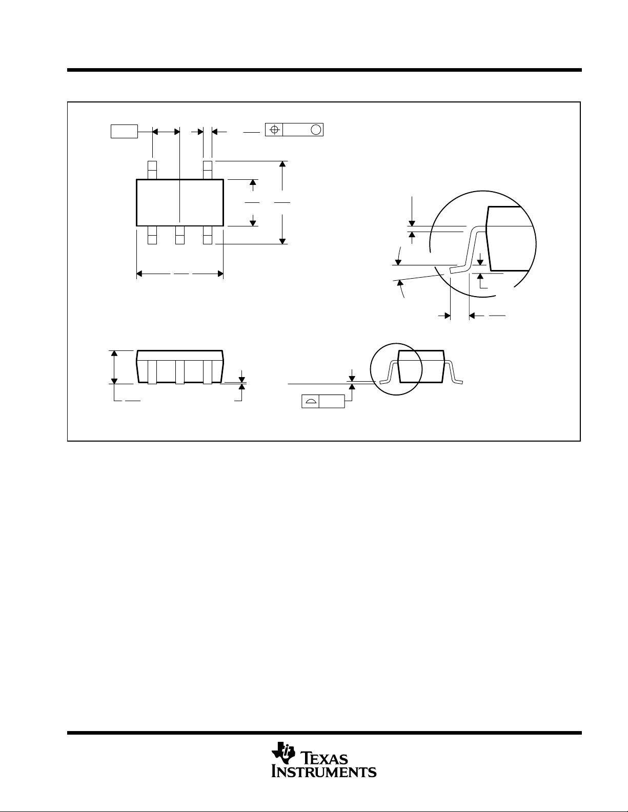
MECHANICAL DATA
MPDS018E – FEBRUARY 1996 – REVISED FEBRUARY 2002
DBV (R-PDSO-G5) PLASTIC SMALL-OUTLINE
0,95
1,45
0,95
3,00
2,80
45
31
0,05 MIN
5X
0,50
0,30
1,70
1,50
0,20
3,00
2,60
Seating Plane
M
0,15 NOM
Gage Plane
0,25
0°–8°
0,10
0,55
0,35
NOTES: A. All linear dimensions are in millimeters.
B. This drawing is subject to change without notice.
C. Body dimensions do not include mold flash or protrusion.
D. Falls within JEDEC MO-178
4073253-4/G 01/02
POST OFFICE BOX 655303 • DALLAS, TEXAS 75265
1
Page 8

MECHANICAL DATA
MPDS025C – FEBRUARY 1997 – REVISED FEBRUARY 2002
DCK (R-PDSO-G5) PLASTIC SMALL-OUTLINE P ACKAGE
0,65
1,10
0,80
1 3
2,15
1,85
45
0,10
0,00
0,30
0,15
1,40
1,10
0,10
2,40
1,80
Seating Plane
M
0,13 NOM
Gage Plane
0,15
0°–8°
0,10
0,46
0,26
NOTES: A. All linear dimensions are in millimeters.
B. This drawing is subject to change without notice.
C. Body dimensions do not include mold flash or protrusion.
D. Falls within JEDEC MO-203
4093553-2/D 01/02
POST OFFICE BOX 655303 • DALLAS, TEXAS 75265
1
Page 9
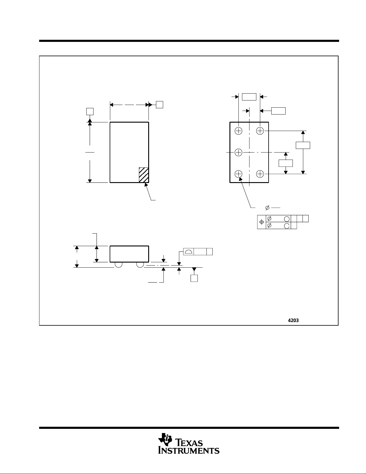
MECHANICAL DATA
MXBG001B AUGUST 2001 – REVISED MA Y 2002
YEA (R–XBGA–N5) DIE–SIZE BALL GRID ARRAY
0,35 MAX
0,50 MAX
A
1,45
1,35
0,95
0,85
B
PIN A1 INDEX AREA
0,05
C
B
A
1
C
SEATING PLANE
0,50
5X
0,25
1,00
0,50
2
0,19
0,15
M
0,05
0,05
M
BCA
C
NOTES: A. All linear dimensions are in millimeters.
B. This drawing is subject to change without notice.
C. NanoStar package configuration.
D. Package complies to JEDEC MO–211 variation EA.
E. This package is tin–lead (SnPb). Refer to the 5 YZA package (drawing 4204151) for lead–free.
0,15
0,10
C
4203167–2/C 04/2002
POST OFFICE BOX 655303 • DALLAS, TEXAS 75265
1
Page 10

MECHANICAL DATA
MXBG004A – JANUARY 2002 – REVISED APRIL 2002
YZA (R-XBGA-N5) DIE-SIZE BALL GRID ARRAY
0,35 MAX
0,50 MAX
A
1,45
1,35
0,95
0,85
B
Pin A1 Index Area
0,05
C
Seating Plane
0,50
0,25
C
1,00
B
0,50
A
5X
2
0,19
0,15
M
0,05
0,05
M
BCA
C
1
NOTES: A. All linear dimensions are in millimeters.
B. This drawing is subject to change without notice.
C. NanoFree package configuration.
D. Package complies to JEDEC MO-211 variation EA.
E. This package is lead-free. Refer to the 5 YEA package (drawing 4203167) for tin-lead (SnPb).
NanoFree is a trademark of Texas Instruments.
0,15
0,10
C
4204151-2/B 03/2002
POST OFFICE BOX 655303 • DALLAS, TEXAS 75265
1
Page 11

IMPORTANT NOTICE
Texas Instruments Incorporated and its subsidiaries (TI) reserve the right to make corrections, modifications,
enhancements, improvements, and other changes to its products and services at any time and to discontinue
any product or service without notice. Customers should obtain the latest relevant information before placing
orders and should verify that such information is current and complete. All products are sold subject to TI’s terms
and conditions of sale supplied at the time of order acknowledgment.
TI warrants performance of its hardware products to the specifications applicable at the time of sale in
accordance with TI’s standard warranty . Testing and other quality control techniques are used to the extent TI
deems necessary to support this warranty . Except where mandated by government requirements, testing of all
parameters of each product is not necessarily performed.
TI assumes no liability for applications assistance or customer product design. Customers are responsible for
their products and applications using TI components. T o minimize the risks associated with customer products
and applications, customers should provide adequate design and operating safeguards.
TI does not warrant or represent that any license, either express or implied, is granted under any TI patent right,
copyright, mask work right, or other TI intellectual property right relating to any combination, machine, or process
in which TI products or services are used. Information published by TI regarding third–party products or services
does not constitute a license from TI to use such products or services or a warranty or endorsement thereof.
Use of such information may require a license from a third party under the patents or other intellectual property
of the third party , or a license from TI under the patents or other intellectual property of TI.
Reproduction of information in TI data books or data sheets is permissible only if reproduction is without
alteration and is accompanied by all associated warranties, conditions, limitations, and notices. Reproduction
of this information with alteration is an unfair and deceptive business practice. TI is not responsible or liable for
such altered documentation.
Resale of TI products or services with statements different from or beyond the parameters stated by TI for that
product or service voids all express and any implied warranties for the associated TI product or service and
is an unfair and deceptive business practice. TI is not responsible or liable for any such statements.
Mailing Address:
Texas Instruments
Post Office Box 655303
Dallas, Texas 75265
Copyright 2003, Texas Instruments Incorporated
 Loading...