

Texas Instruments SN74LVC10ADBR, SN74LVC10ADR, SN74LVC10APWLE, SN74LVC10APWR, SN74LVC10AD Datasheet
...
SN74LVC10A
TRIPLE 3-INPUT POSITIVE-NAND GATE
SCAS284G – JANUARY 1993 – REVISED OCTOBER 1998
D
EPIC
(Enhanced-Performance Implanted
CMOS) Submicron Process
D
ESD Protection Exceeds 2000 V Per
MIL-STD-883, Method 3015; Exceeds 200 V
Using Machine Model (C = 200 pF, R = 0)
D
Latch-Up Performance Exceeds 250 mA Per
JESD 17
D
Typical V
< 0.8 V at V
D
Typical V
> 2 V at V
D
Inputs Accept Voltages to 5.5 V
D
Package Options Include Plastic
(Output Ground Bounce)
OLP
= 3.3 V, TA = 25°C
CC
(Output VOH Undershoot)
OHV
= 3.3 V, TA = 25°C
CC
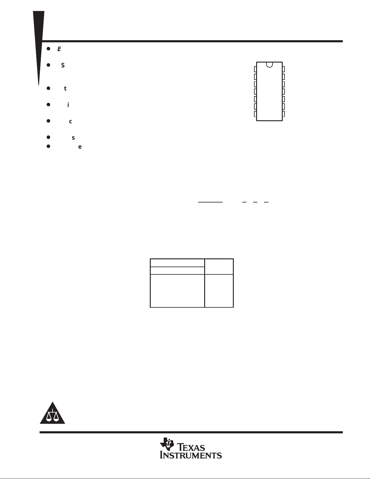
D, DB, OR PW PACKAGE
(TOP VIEW)
1A
1B
2A
2B
2C
2Y
GND
1
2
3
4
5
6
7
14
13
12
11
10
V
1C
1Y
3C
3B
3A
9
3Y
8
CC
Small-Outline (D), Shrink Small-Outline
(DB), and Thin Shrink Small-Outline (PW)
Packages
description
This triple 3-input positive-NAND gate is designed for 1.65-V to 3.6-V VCC operation.
The SN74LVC10A performs the Boolean function Y = A
Inputs can be driven from either 3.3-V or 5-V devices. This feature allows the use of these devices as translators
in a mixed 3.3-V/5-V system environment.
• B • C or Y = A + B + C in positive logic.
The SN74LVC10A is characterized for operation from –40°C to 85°C.
FUNCTION TABLE
(each gate)
INPUTS
A B C
H H H L
L XX H
XLX H
XXL H
OUTPUT
Y
Please be aware that an important notice concerning availability, standard warranty, and use in critical applications of
Texas Instruments semiconductor products and disclaimers thereto appears at the end of this data sheet.
EPIC is a trademark of Texas Instruments Incorporated.
PRODUCTION DATA information is current as of publication date.
Products conform to specifications per the terms of Texas Instruments
standard warranty. Production processing does not necessarily include
testing of all parameters.
POST OFFICE BOX 655303 • DALLAS, TEXAS 75265
Copyright 1998, Texas Instruments Incorporated
1
SN74LVC10A
TRIPLE 3-INPUT POSITIVE-NAND GATE
SCAS284G – JANUARY 1993 – REVISED OCTOBER 1998
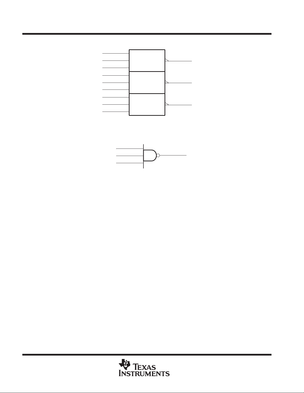
logic symbol
†
This symbol is in accordance with ANSI/IEEE Std 91-1984 and IEC Publication 617-12.
†
1A
1B
1C
2A
2B
2C
3A
3B
3C
1
2
13
3
4
5
9
10
11
&
12
1Y
6
2Y
8
3Y
logic diagram, each gate (positive logic)
A
B
C
Y
absolute maximum ratings over operating free-air temperature range (unless otherwise noted)
‡
Supply voltage range, V
Input voltage range, V
Output voltage range, V
Input clamp current, I
Output clamp current, I
Continuous output current, I
Continuous current through V
Package thermal impedance, θ
–0.5 V to 6.5 V. . . . . . . . . . . . . . . . . . . . . . . . . . . . . . . . . . . . . . . . . . . . . . . . . . . . . . . . .
CC
(see Note 1) –0.5 V to 6.5 V. . . . . . . . . . . . . . . . . . . . . . . . . . . . . . . . . . . . . . . . . . . . . . . . .
I
(see Notes 1 and 2) –0.5 V to VCC + 0.5 V. . . . . . . . . . . . . . . . . . . . . . . . . . . . . . . . . .
O
(VI < 0) –50 mA. . . . . . . . . . . . . . . . . . . . . . . . . . . . . . . . . . . . . . . . . . . . . . . . . . . . . . . . . . .
IK
(VO < 0) –50 mA. . . . . . . . . . . . . . . . . . . . . . . . . . . . . . . . . . . . . . . . . . . . . . . . . . . . . . . .
OK
±50 mA. . . . . . . . . . . . . . . . . . . . . . . . . . . . . . . . . . . . . . . . . . . . . . . . . . . . . . . . . . . . .
O
or GND ±100 mA. . . . . . . . . . . . . . . . . . . . . . . . . . . . . . . . . . . . . . . . . . . . . . . . . .
CC
(see Note 3): D package 127°C/W. . . . . . . . . . . . . . . . . . . . . . . . . . . . . . . . . .
JA
DB package 158°C/W. . . . . . . . . . . . . . . . . . . . . . . . . . . . . . . .
PW package 170°C/W. . . . . . . . . . . . . . . . . . . . . . . . . . . . . . . .
Storage temperature range, T
‡
Stresses beyond those listed under “absolute maximum ratings” may cause permanent damage to the device. These are stress ratings only, and
functional operation of the device at these or any other conditions beyond those indicated under “recommended operating conditions” is not
implied. Exposure to absolute-maximum-rated conditions for extended periods may affect device reliability.
NOTES: 1. The input negative-voltage and output voltage ratings may be exceeded if the input and output current ratings are observed.
2. The value of VCC is provided in the recommended operating conditions table.
3. The package thermal impedance is calculated in accordance with JESD 51.
–65°C to 150°C. . . . . . . . . . . . . . . . . . . . . . . . . . . . . . . . . . . . . . . . . . . . . . . . . . .
stg
2
POST OFFICE BOX 655303 • DALLAS, TEXAS 75265
VCCSuppl
oltage
V
IOHHigh-level output current
mA
IOLLow-level output current
mA
V
V
I
mA
SN74LVC10A
TRIPLE 3-INPUT POSITIVE-NAND GATE
SCAS284G – JANUARY 1993 – REVISED OCTOBER 1998
recommended operating conditions (see Note 4)
MIN MAX UNIT
pp
y v
V
V
V
V
T
NOTE 4: All unused inputs of the device must be held at VCC or GND to ensure proper device operation. Refer to the TI application report,
High-level input voltage
IH
Low-level input voltage
IL
Input voltage 0 5.5 V
I
Output voltage 0 V
O
p
p
Operating free-air temperature –40 85 °C
A
Implications of Slow or Floating CMOS Inputs
, literature number SCBA004.
Operating 1.65 3.6
Data retention only 1.5
VCC = 1.65 V to 1.95 V 0.65 × V
VCC = 2.3 V to 2.7 V
VCC = 2.7 V to 3.6 V 2
VCC = 1.65 V to 1.95 V 0.35 × V
VCC = 2.3 V to 2.7 V 0.7
VCC = 2.7 V to 3.6 V 0.8
VCC = 1.65 V –4
VCC = 2.3 V –8
VCC = 2.7 V –12
VCC = 3 V –24
VCC = 1.65 V 4
VCC = 2.3 V 8
VCC = 2.7 V 12
VCC = 3 V 24
CC
1.7
CC
V
CC
V
V
electrical characteristics over recommended operating free-air temperature range (unless
otherwise noted)
PARAMETER TEST CONDITIONS
IOH = –100 µA 1.65 V to 3.6 V VCC–0.2
IOH = –4 mA 1.65 V 1.2
OH
V
OL
I
I
I
CC
∆I
CC
C
†
All typical values are at VCC = 3.3 V, TA = 25°C.
i
IOH = –8 mA 2.3 V 1.7
= –12
OH
IOH = –24 mA 3 V 2.2
IOL = 100 µA 1.65 V to 3.6 V 0.2
IOL = 4 mA 1.65 V 0.45
IOL = 8 mA 2.3 V 0.7
IOL = 12 mA 2.7 V 0.4
IOL = 24 mA 3 V 0.55
VI = 5.5 V or GND 3.6 V ±5 µA
VI = VCC or GND, IO = 0 3.6 V 10 µA
One input at VCC – 0.6 V, Other inputs at VCC or GND 2.7 V to 3.6 V 500 µA
VI = VCC or GND 3.3 V 5 pF
V
CC
2.7 V 2.2
3 V 2.4
MIN TYP†MAX UNIT
V
POST OFFICE BOX 655303 • DALLAS, TEXAS 75265
3
 Loading...