

Datasheet SN74LV594ADR, SN74LV594ANSR, SN74LV594APWR, SN74LV594AD, SN74LV594ADBR Datasheet (Texas Instruments)
SN54LV594A, SN74LV594A
8-BIT SHIFT REGISTERS
WITH OUTPUT REGISTERS
SCLS413B – APRIL 1998 – REVISED SEPTEMBER 1999
D
EPIC
(Enhanced-Performance
Implanted CMOS) Process
D
Typical V
(Output Ground Bounce)
OLP
<0.8 V at VCC = 3.3 V, TA = 25°C
D
Typical V
>2 V at V
D
8-Bit Serial-In, Parallel-Out Shift
(Output VOH Undershoot)
OHV
= 3.3 V, TA = 25°C
CC
Registers With Storage
D
Independent Direct Overriding Clears
on Shift and Storage Registers
D
Independent Clocks for Shift and
Storage Registers
D
Latch-Up Performance Exceeds 100 mA
Per JESD 78, Class II
D
ESD Protection Exceeds JESD 22
– 2000-V Human-Body Model (A114-A)
– 200-V Machine Model (A115-A)
– 1000-V Charged-Device Model (C101)
D
Package Options Include Plastic
Small-Outline (D, NS), Shrink
Small-Outline (DB), and Thin Shrink
Small-Outline (PW) Packages, Ceramic
Flat (W) Packages, Chip Carriers (FK),
and DIPs (J)
description
The ’LV594A devices are 8-bit shift registers
designed for 2-V to 5.5-V VCC operation.
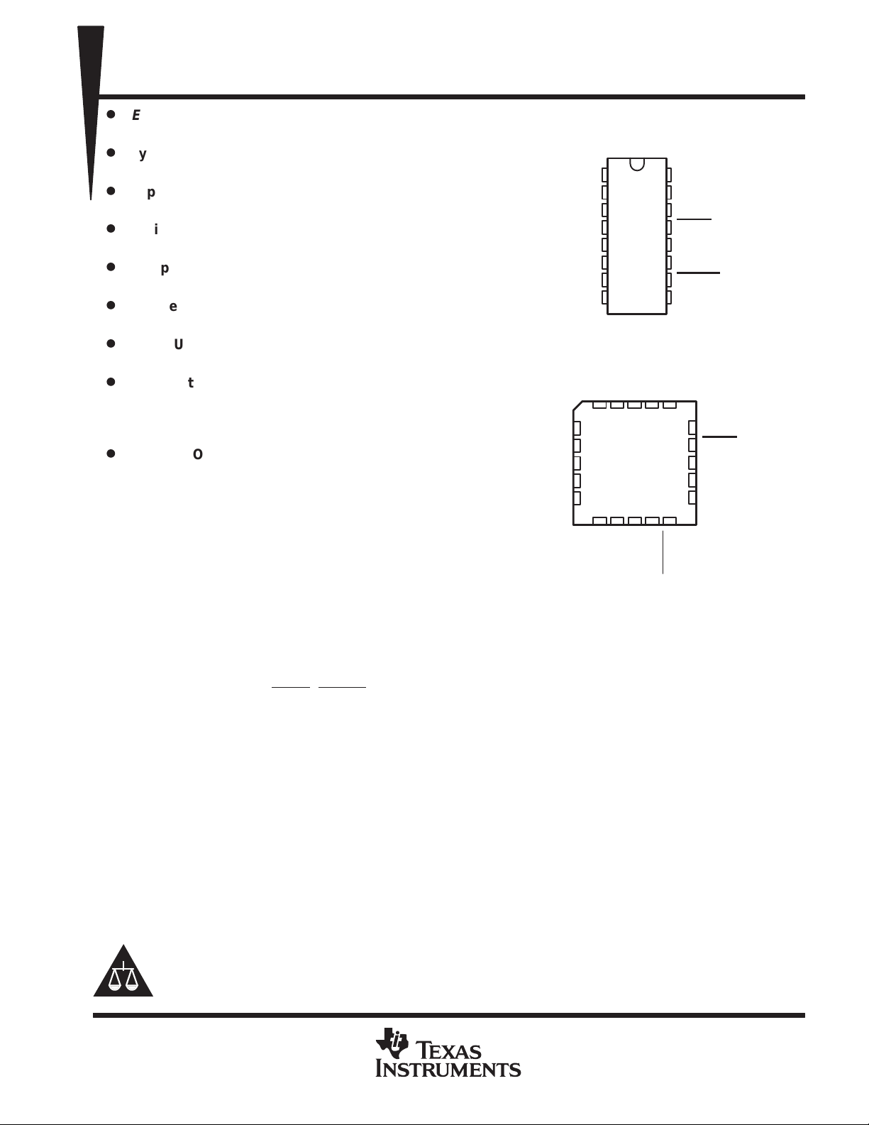
SN54LV594A...J OR W PACKAGE
SN74LV594A. . . D, DB, NS, OR PW PACKAGE
SN54LV594A. . . FK PACKAGE
Q
D
Q
E
NC
Q
F
Q
G
NC – No internal connection
(TOP VIEW)
Q
1
B
Q
2
C
Q
3
D
Q
4
E
5
Q
F
6
Q
G
7
Q
H
GND
8
(TOP VIEW)
CQB
Q
3212019
4
5
6
7
8
910111213
H
Q
NC
NC
GND
16
15
14
13
12
11
10
9
VCCQ
′
H
Q
V
CC
Q
A
SER
RCLR
RCLK
SRCLK
SRCLR
Q
H′
A
SER
18
RCLR
17
NC
16
RCLK
15
14
SRCLK
SRCLR
These devices contain an 8-bit serial-in, parallelout shift register that feeds an 8-bit D-type storage
register. Separate clocks (RCLK, SRCLK) and
direct overriding clear (RCLR, SRCLR) inputs are provided on the shift and storage registers. A serial output
(QH′) is provided for cascading purposes.
The shift-register (SRCLK) and storage-register (RCLK) clocks are positive-edge triggered. If the clocks are tied
together, the shift register always is one clock pulse ahead of the storage register.
The SN54LV594A is characterized for operation over the full military temperature range of –55°C to 125°C.
The SN74LV594A is characterized for operation from –40°C to 85°C.
Please be aware that an important notice concerning availability, standard warranty, and use in critical applications of
Texas Instruments semiconductor products and disclaimers thereto appears at the end of this data sheet.
EPIC is a trademark of Texas Instruments Incorporated.
UNLESS OTHERWISE NOTED this document contains PRODUCTION
DATA information current as of publication date. Products conform to
specifications per the terms of Texas Instruments standard warranty.
Production processing does not necessarily include testing of all
parameters.
Copyright 1999, Texas Instruments Incorporated
POST OFFICE BOX 655303 • DALLAS, TEXAS 75265
1
SN54LV594A, SN74LV594A
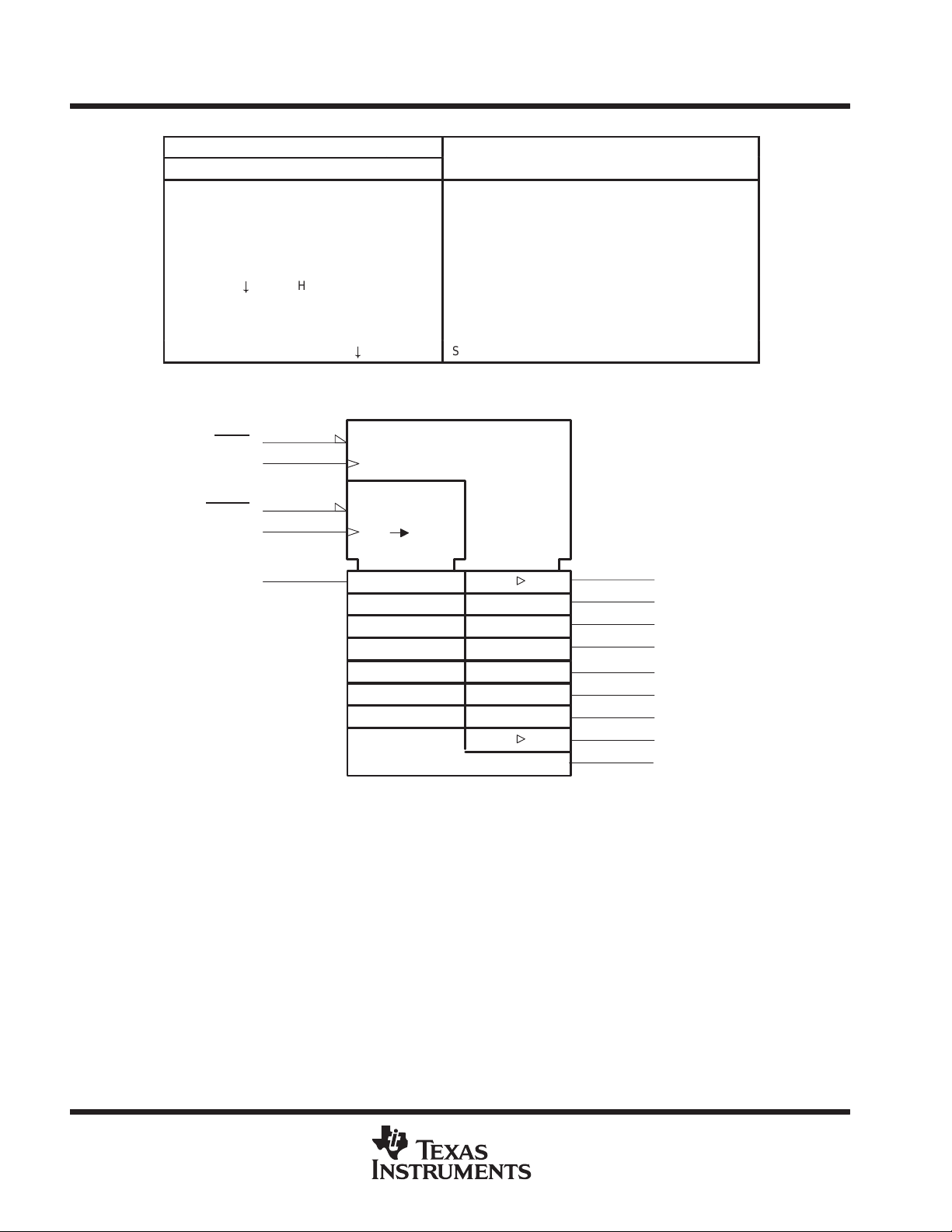
FUNCTION
8-BIT SHIFT REGISTERS
WITH OUTPUT REGISTERS
SCLS413B – APRIL 1998 – REVISED SEPTEMBER 1999
INPUTS
SER SRCLK SRCLR RCLK RCLR
X X L X X Shift register is cleared.
L ↑ HXX
H ↑ HXX
L
X X X X L Storage register is cleared.
X XX↑ H Shift register data is stored in the storage register.
X X X
#
H X X Shift register state is not changed.
FUNCTION TABLE
First stage of shift register goes low. Other stages
store the data of previous stage, respectively.
First stage of shift register goes high. Other stages
store the data of previous stage, respectively.
#
H Storage register state is not changed.
logic symbol
†
This symbol is in accordance with ANSI/IEEE Std 91-1984 and IEC Publication 617-12.
Pin numbers shown are for the D, DB, J, NS, PW, and W packages.
†
SER
13
12
10
11
14
RCLR
RCLK C2
SRCLR
SRCLK
R3
R
1D
SRG8
C1/
2D
2D
15
3
3
Q
A
1
Q
B
2
Q
C
3
Q
D
4
Q
E
5
Q
F
6
Q
G
7
Q
H
9
Q
H′
2
POST OFFICE BOX 655303 • DALLAS, TEXAS 75265
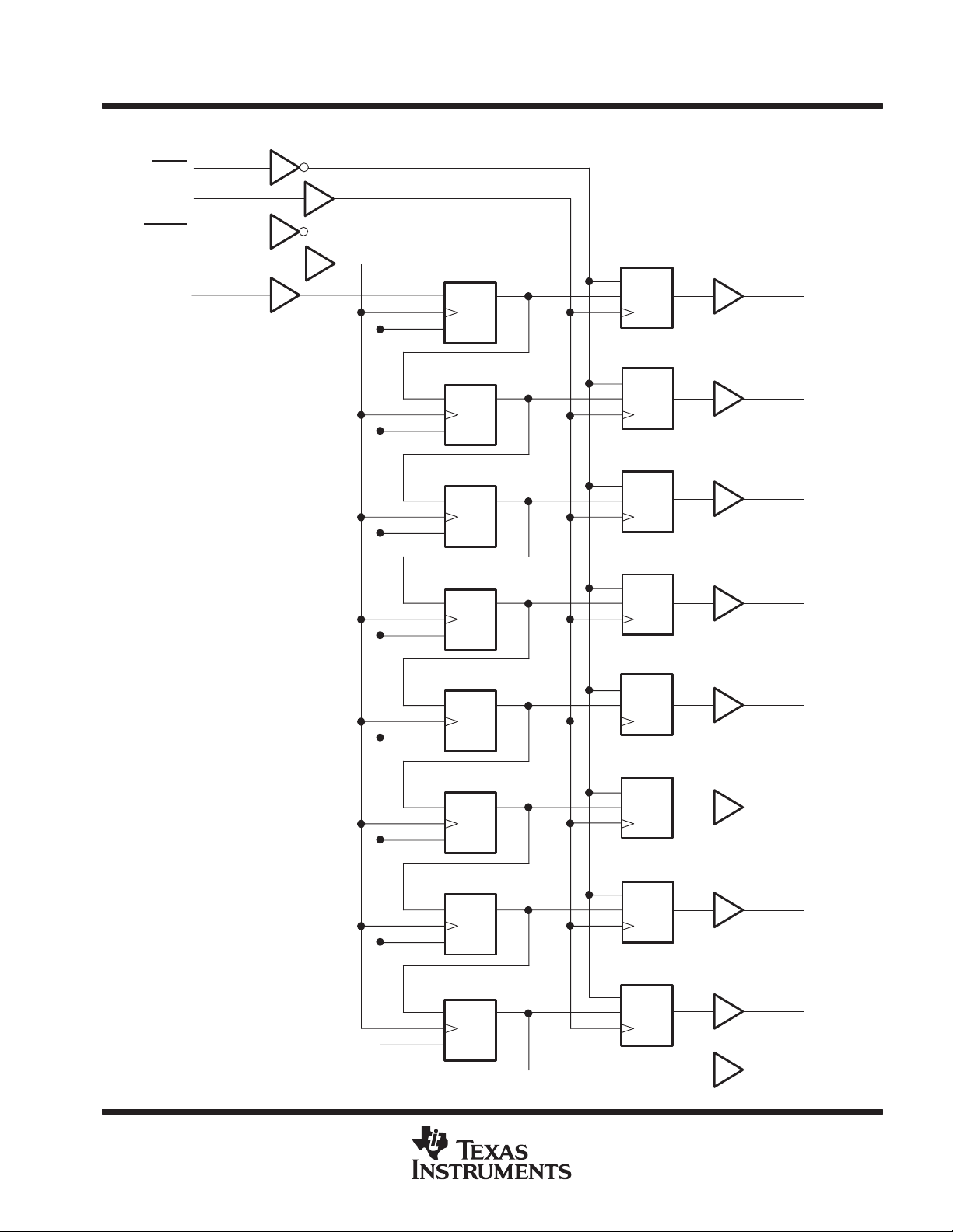
logic diagram (positive logic)
SN54LV594A, SN74LV594A
8-BIT SHIFT REGISTERS
WITH OUTPUT REGISTERS
SCLS413B – APRIL 1998 – REVISED SEPTEMBER 1999
RCLR
RCLK
SRCLR
SRCLK
SER
13
12
10
11
14
1D
R
2D
R
2D
R
2D
R
C1
C2
C2
C2
Q
Q
Q
Q
R
3D
R
3D
R
3D
R
3D
Q
C3
Q
C3
Q
C3
Q
C3
15
Q
A
1
Q
B
2
Q
C
3
Q
D
2D
C2
R
2D
C2
R
2D
C2
R
2D
C2
R
Pin numbers shown are for the D, DB, J, NS, PW, and W packages.
Q
Q
Q
Q
R
3D
R
3D
R
3D
R
3D
Q
C3
Q
C3
Q
C3
Q
C3
4
Q
E
5
Q
F
6
Q
G
7
Q
H
9
Q
H′
POST OFFICE BOX 655303 • DALLAS, TEXAS 75265
3
SN54LV594A, SN74LV594A
8-BIT SHIFT REGISTERS
WITH OUTPUT REGISTERS
SCLS413B – APRIL 1998 – REVISED SEPTEMBER 1999
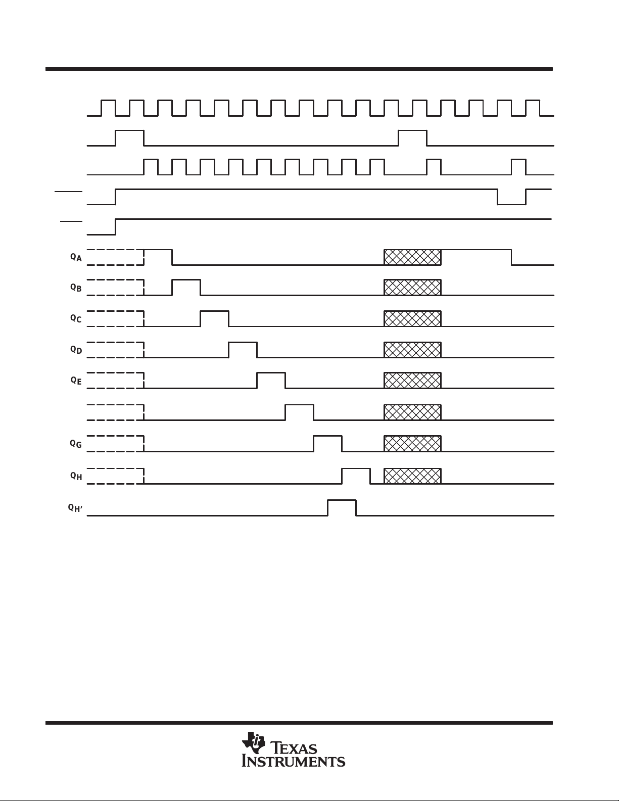
timing diagram
SRCLK
SER
RCLK
SRCLR
RCLR
Q
A
Q
B
Q
C
Q
D
Q
E
Q
F
Q
G
Q
H
Q
H’
4
POST OFFICE BOX 655303 • DALLAS, TEXAS 75265

UNIT
VIHHigh-level input voltage
V
VILLow-level input voltage
V
IOHHigh-level output current
IOLLow-level output current
SN54LV594A, SN74LV594A
8-BIT SHIFT REGISTERS
WITH OUTPUT REGISTERS
SCLS413B – APRIL 1998 – REVISED SEPTEMBER 1999
absolute maximum ratings over operating free-air temperature range (unless otherwise noted)
†
Supply voltage range, VCC –0.5 V to 7 V. . . . . . . . . . . . . . . . . . . . . . . . . . . . . . . . . . . . . . . . . . . . . . . . . . . . . . . . . .
Input voltage range, VI (see Note 1) –0.5 V to 7 V. . . . . . . . . . . . . . . . . . . . . . . . . . . . . . . . . . . . . . . . . . . . . . . . . .
Output voltage range, V
(see Notes 1 and 2) –0.5 V to VCC + 0.5 V. . . . . . . . . . . . . . . . . . . . . . . . . . . . . . . . . .
O
Input clamp current, IIK (VI < 0) –20 mA. . . . . . . . . . . . . . . . . . . . . . . . . . . . . . . . . . . . . . . . . . . . . . . . . . . . . . . . . . .
Output clamp current, IOK (VO < 0 or VO > VCC) ±50 mA. . . . . . . . . . . . . . . . . . . . . . . . . . . . . . . . . . . . . . . . . . . .
Continuous output current, IO (VO = 0 to VCC) ±35 mA. . . . . . . . . . . . . . . . . . . . . . . . . . . . . . . . . . . . . . . . . . . . . .
Continuous current through VCC or GND ±70 mA. . . . . . . . . . . . . . . . . . . . . . . . . . . . . . . . . . . . . . . . . . . . . . . . . . .
Package thermal impedance, θ
(see Note 3): D package 73°C/W. . . . . . . . . . . . . . . . . . . . . . . . . . . . . . . . . . .
JA
DB package 82°C/W. . . . . . . . . . . . . . . . . . . . . . . . . . . . . . . . . .
NS package 64°C/W. . . . . . . . . . . . . . . . . . . . . . . . . . . . . . . . . .
PW package 108°C/W. . . . . . . . . . . . . . . . . . . . . . . . . . . . . . . .
Storage temperature range, T
†
Stresses beyond those listed under “absolute maximum ratings” may cause permanent damage to the device. These are stress ratings only, and
functional operation of the device at these or any other conditions beyond those indicated under “recommended operating conditions” is not
implied. Exposure to absolute-maximum-rated conditions for extended periods may affect device reliability.
NOTES: 1. The input and output voltage ratings may be exceeded if the input and output current ratings are observed.
2. This value is limited to 7 V maximum.
3. The package thermal impedance is calculated in accordance with JESD 51.
–65°C to 150°C. . . . . . . . . . . . . . . . . . . . . . . . . . . . . . . . . . . . . . . . . . . . . . . . . . .
stg
recommended operating conditions (see Note 4)
SN54LV594A SN74LV594A
MIN MAX MIN MAX
V
V
V
∆t/∆v Input transition rise or fall rate
T
NOTE 4: All unused inputs of the device must be held at VCC or GND to ensure proper device operation. Refer to the TI application report,
Supply voltage 2 5.5 2 5.5 V
CC
VCC = 2 V 1.5 1.5
p
p
Input voltage 0 5.5 0 5.5 V
I
Output voltage 0 V
O
p
p
Operating free-air temperature –55 125 –40 85 °C
A
Implications of Slow or Floating CMOS Inputs
VCC = 2.3 V to 2.7 V VCC× 0.7 VCC× 0.7
VCC = 3 V to 3.6 V VCC× 0.7 VCC× 0.7
VCC = 4.5 V to 5.5 V VCC× 0.7 VCC× 0.7
VCC = 2 V 0.5 0.5
VCC = 2.3 V to 2.7 V VCC× 0.3 VCC× 0.3
VCC = 3 V to 3.6 V VCC× 0.3 VCC× 0.3
VCC = 4.5 V to 5.5 V VCC× 0.3 VCC× 0.3
CC
VCC = 2 V –50 –50 µA
VCC = 2.3 V to 2.7 V –2 –2
VCC = 3 V to 3.6 V –6 –6
VCC = 4.5 V to 5.5 V –12 –12
VCC = 2 V 50 50 µA
VCC = 2.3 V to 2.7 V 2 2
VCC = 3 V to 3.6 V 6 6
VCC = 4.5 V to 5.5 V 12 12
VCC = 2.3 V to 2.7 V 0 200 0 200
VCC = 3 V to 3.6 V
VCC = 4.5 V to 5.5 V 0 20 0 20
, literature number SCBA004.
0 100 0 100
0 V
CC
V
mA
mA
ns/V
PRODUCT PREVIEW information concerns products in the formative or
design phase of development. Characteristic data and other
specifications are design goals. Texas Instruments reserves the right to
change or discontinue these products without notice.
POST OFFICE BOX 655303 • DALLAS, TEXAS 75265
5

SN54LV594A, SN74LV594A
PARAMETER
TEST CONDITIONS
V
UNIT
V
V
V
V
C
V
V
GND
pF
UNIT
twPulse duration
ns
UNIT
twPulse duration
ns
8-BIT SHIFT REGISTERS
WITH OUTPUT REGISTERS
SCLS413B – APRIL 1998 – REVISED SEPTEMBER 1999
electrical characteristics over recommended operating free-air temperature range (unless
otherwise noted)
SN54LV594A SN74LV594A
MIN TYP MAX MIN TYP MAX
p
I
I
I
OH
OL
I
CC
off
i
CC
IOH = –50 µA 2 V to 5.5 V VCC–0.1 VCC–0.1
IOH = –2 mA 2.3 V 2 2
IOH = –6 mA 3 V 2.48 2.48
IOH = –12 mA 4.5 V 3.8 3.8
IOL = 50 µA 2 V to 5.5 V 0.1 0.1
IOL = 2 mA 2.3 V 0.4 0.4
IOL = 6 mA 3 V 0.44 0.44
IOL = 12 mA 4.5 V 0.55 0.55
VI = VCC or GND 5.5 V ±1 ±1 µA
VI = VCC or GND, IO = 0 5.5 V 20 20 µA
VI or VO = 0 to 5.5 V 0 V 5 5 µA
=
or
I
CC
3.3 V 3.5 3.5
5 V 2 2
timing requirements over recommended operating free-air temperature range, V
= 2.5 V± 0.2 V
CC
(unless otherwise noted) (see Figure 1)
TA = 25°C SN54LV594A SN74LV594A
MIN MAX MIN MAX MIN MAX
RCLK or SRCLK high or low 7 7.5 7.5
RCLR or SRCLR low 6 6.5 6.5
SER before SRCLK↑ 2.5 3 3
SRCLK↑ before RCLK↑
t
su
t
h
†
This setup time ensures the output register sees stable data from the shift-register outputs. The clocks can be tied together, in which case the
shift register is one clock pulse ahead of the storage register.
Setup time
Hold time SER after SRCLK↑ 1.5 1.5 1.5 ns
SRCLR low before RCLK↑ 8.5 9.5 9.5
SRCLR high (inactive) before SRCLK↑ 6 6.8 6.8
RCLR high (inactive) before RCLK↑ 6.7 7.6 7.6
timing requirements over recommended operating free-air temperature range, V
†
8 9 9
CC
ns
= 3.3 V ± 0.3 V
(unless otherwise noted) (see Figure 1)
TA = 25°C SN54LV594A SN74LV594A
MIN MAX MIN MAX MIN MAX
RCLK or SRCLK high or low 5.5 5.5 5.5
RCLR or SRCLR low 5 5 5
SER before SRCLK↑ 3.5 3.5 3.5
SRCLK↑ before RCLK↑
t
su
t
h
†
This setup time ensures the output register sees stable data from the shift-register outputs. The clocks can be tied together, in which case the
shift register is one clock pulse ahead of the storage register.
Setup time
Hold time SER after SRCLK↑ 1.5 1.5 1.5 ns
low before RCLK↑ 8 9 9
SRCLR
SRCLR high (inactive) before SRCLK↑ 4.2 4.8 4.8
RCLR high (inactive) before RCLK↑ 4.6 5.3 5.3
†
8 8.5 8.5
ns
PRODUCT PREVIEW information concerns products in the formative or
design phase of development. Characteristic data and other
specifications are design goals. Texas Instruments reserves the right to
change or discontinue these products without notice.
6
POST OFFICE BOX 655303 • DALLAS, TEXAS 75265

UNIT
twPulse duration
ns
PARAMETER
UNIT
f
MH
RCLK
Q
Q
SRCLK
Q
C
F
RCLK
Q
Q
SRCLK
Q
C
F
SN54LV594A, SN74LV594A
8-BIT SHIFT REGISTERS
WITH OUTPUT REGISTERS
SCLS413B – APRIL 1998 – REVISED SEPTEMBER 1999
timing requirements over recommended operating free-air temperature range, V
= 5 V ± 0.5 V
CC
(unless otherwise noted) (see Figure 1)
TA = 25°C SN54LV594A SN74LV594A
MIN MAX MIN MAX MIN MAX
RCLK or SRCLK high or low 5 5 5
RCLR or SRCLR low 5.2 5.2 5.2
SER before SRCLK↑ 3 3 3
SRCLK↑ before RCLK↑
t
su
t
h
†
This setup time ensures the output register sees stable data from the shift-register outputs. The clocks can be tied together, in which case the
shift register is one clock pulse ahead of the storage register.
Setup time
Hold time SER after SRCLK↑ 2 2 2 ns
SRCLR low before RCLK↑ 5 5 5
SRCLR high (inactive) before SRCLK↑ 2.9 3.3 3.3
RCLR high (inactive) before RCLK↑ 3.2 3.7 3.7
†
5 5 5
ns
switching characteristics over recommended operating free-air temperature range,
= 2.5 V ± 0.2 V (unless otherwise noted) (see Figure 1)
V
CC
FROM TO LOAD
(INPUT) (OUTPUT) CAPACITANCE
max
t
*
PLH
t
*
PHL
t
*
PLH
t
*
PHL
t
*
PHL
t
*
PHL
t
PLH
t
PHL
t
PLH
t
PHL
t
PHL
t
PHL
* On products compliant to MIL-PRF-38535, this parameter is not production tested.
RCLR QA–Q
SRCLR Q
RCLR QA–Q
SRCLR Q
–
A
H
H′
H
H′
–
A
H
H′
H
H′
CL = 15 pF* 65 80 45 45
CL = 50 pF 60 70 40 40
= 15 p
L
= 50 p
L
TA = 25°C SN54LV594A SN74LV594A
MIN TYP MAX MIN MAX MIN MAX
6.4 10.6 1 11.1 1 11.1
6.3 10.4 1 11.1 1 11.1
7.4 12.1 1 12.8 1 12.8
7.2 11.6 1 12.8 1 12.8
7.9 12.7 1 13.6 1 13.6
7.4 11.9 1 13.1 1 13.1
9.5 14.1 1 14.6 1 14.6
10.8 15.5 1 17.2 1 17.2
10.6 15.7 1 16.5 1 16.5
11.3 16.1 1 18.6 1 18.6
12.1 17.4 1 19 1 19
11.6 16.5 1 18.6 1 18.6
ns
ns
z
PRODUCT PREVIEW information concerns products in the formative or
design phase of development. Characteristic data and other
specifications are design goals. Texas Instruments reserves the right to
change or discontinue these products without notice.
POST OFFICE BOX 655303 • DALLAS, TEXAS 75265
7

SN54LV594A, SN74LV594A
PARAMETER
UNIT
f
MH
RCLK
Q
Q
SRCLK
Q
C
F
RCLK
Q
Q
SRCLK
Q
C
F
PARAMETER
UNIT
f
MH
RCLK
Q
Q
SRCLK
Q
C
F
RCLK
Q
Q
SRCLK
Q
C
50 pF
8-BIT SHIFT REGISTERS
WITH OUTPUT REGISTERS
SCLS413B – APRIL 1998 – REVISED SEPTEMBER 1999
switching characteristics over recommended operating free-air temperature range,
V
= 3.3 V ± 0.3 V (unless otherwise noted) (see Figure 1)
CC
FROM TO LOAD
(INPUT) (OUTPUT) CAPACITANCE
max
t
*
PLH
t
*
PHL
t
*
PLH
t
*
PHL
t
*
PHL
t
*
PHL
t
PLH
t
PHL
t
PLH
t
PHL
t
PHL
t
PHL
* On products compliant to MIL-PRF-38535, this parameter is not production tested.
RCLR QA–Q
SRCLR Q
RCLR QA–Q
SRCLR Q
–
A
H
H′
H
H′
–
A
H
H′
H
H′
CL = 15 pF* 80 120 70 70
CL = 50 pF 55 105 50 50
= 15 p
L
= 50 p
L
TA = 25°C SN54LV594A SN74LV594A
MIN TYP MAX MIN MAX MIN MAX
4.6 8 1 8.5 1 8.5
4.9 8.2 1 8.8 1 8.8
5.4 9.1 1 9.7 1 9.7
5.5 9.2 1 9.9 1 9.9
6 9.8 1 10.6 1 10.6
5.6 9.2 1 10 1 10
6.9 10.5 1 11.1 1 11.1
8.1 11.9 1 13.1 1 13.1
7.7 11.7 1 12.4 1 12.4
8.4 12.5 1 13.9 1 13.9
9.1 13.1 1 14.4 1 14.4
8.5 12.4 1 14 1 14
z
ns
ns
switching characteristics over recommended operating free-air temperature range,
V
= 5 V ± 0.5 V (unless otherwise noted) (see Figure 1)
CC
FROM TO LOAD
(INPUT) (OUTPUT) CAPACITANCE
max
t
*
PLH
t
*
PHL
t
*
PLH
t
*
PHL
t
*
PHL
t
*
PHL
t
PLH
t
PHL
t
PLH
t
PHL
t
PHL
t
PHL
* On products compliant to MIL-PRF-38535, this parameter is not production tested.
RCLR QA–Q
SRCLR Q
RCLR QA–Q
SRCLR Q
–
A
H
H′
H
H′
–
A
H
H′
H
H′
CL = 15 pF* 135 170 115 115
CL = 50 pF 120 140 95 95
= 15 p
L
=
L
TA = 25°C SN54LV594A SN74LV594A
MIN TYP MAX MIN MAX MIN MAX
3.3 6.2 1 6.5 1 6.5
3.7 6.5 1 6.9 1 6.9
3.7 6.8 1 7.2 1 7.2
4.1 7.2 1 7.6 1 7.6
4.5 7.6 1 8.2 1 8.2
4.1 7.1 1 7.6 1 7.6
4.9 7.8 1 8.3 1 8.3
5.8 8.9 1 9.7 1 9.7
5.5 8.6 1 9.1 1 9.1
6 9.2 1 10.1 1 10.1
6.6 10 1 10.7 1 10.7
6 9.2 1 10.1 1 10.1
z
ns
ns
PRODUCT PREVIEW information concerns products in the formative or
design phase of development. Characteristic data and other
specifications are design goals. Texas Instruments reserves the right to
change or discontinue these products without notice.
8
POST OFFICE BOX 655303 • DALLAS, TEXAS 75265

PARAMETER
UNIT
C
d
Power dissi ation ca acitance
f
MHz
F
SN54LV594A, SN74LV594A
8-BIT SHIFT REGISTERS
WITH OUTPUT REGISTERS
SCLS413B – APRIL 1998 – REVISED SEPTEMBER 1999
noise characteristics, V
V
OL(P)
V
OL(V)
V
OH(V)
V
IH(D)
V
IL(D)
NOTE 5: Characteristics are for surface-mount packages only.
Quiet output, maximum dynamic V
Quiet output, minimum dynamic V
Quiet output, minimum dynamic V
High-level dynamic input voltage 2.31 V
Low-level dynamic input voltage 0.99 V
= 3.3 V, CL = 50 pF, TA = 25°C (see Note 5)
CC
OL
OL
OH
operating characteristics, TA = 25°C
PARAMETER TEST CONDITIONS V
p
p
p
= 10
SN74LV594A
MIN TYP MAX
0.5 0.8 V
–0.1 –0.8 V
2.8 V
TYP UNIT
CC
3.3 V 93
5 V 112
p
POST OFFICE BOX 655303 • DALLAS, TEXAS 75265
9

SN54LV594A, SN74LV594A
8-BIT SHIFT REGISTERS
WITH OUTPUT REGISTERS
SCLS413B – APRIL 1998 – REVISED SEPTEMBER 1999
PARAMETER MEASUREMENT INFORMATION
From Output
Under Test
(see Note A)
Test
Point
C
L
From Output
Under Test
(see Note A)
V
RL = 1 kΩ
C
L
S1
CC
Open
GND
TEST S1
t
PLH/tPHL
t
PLZ/tPZL
t
PHZ/tPZH
Open Drain
Open
V
CC
GND
V
CC
LOAD CIRCUIT FOR
TOTEM-POLE OUTPUTS
t
w
Input
Input
In-Phase
Output
Out-of-Phase
Output
INVERTING AND NONINVERTING OUTPUTS
NOTES: A. CL includes probe and jig capacitance.
B. Waveform 1 is for an output with internal conditions such that the output is low except when disabled by the output control.
Waveform 2 is for an output with internal conditions such that the output is high except when disabled by the output control.
C. All input pulses are supplied by generators having the following characteristics: PRR ≤ 1 MHz, ZO = 50 Ω, tr ≤ 3 ns, tf ≤ 3 ns.
D. The outputs are measured one at a time with one input transition per measurement.
E. t
F. t
G. t
50% V
CC
VOLTAGE WAVEFORMS
PULSE DURATION
50% V
CC
t
PLH
50% V
t
PHL
50% V
VOLTAGE WAVEFORMS
PROPAGATION DELAY TIMES
PLZ
PZL
PHL
and t
and t
and t
are the same as t
PHZ
are the same as ten.
PZH
are the same as tpd.
PLH
3-STATE AND OPEN-DRAIN OUTPUTS
50% V
50% V
CC
CC
dis
CC
t
PHL
50% V
t
PLH
50% V
.
LOAD CIRCUIT FOR
V
CC
CC
0 V
V
CC
0 V
V
OH
CC
V
OL
V
OH
CC
V
OL
Timing Input
Data Input
Output
Control
Output
Waveform 1
S1 at V
(see Note B)
Waveform 2
(see Note B)
CC
Output
S1 at GND
50% V
CC
t
CC
CC
h
50% V
50% V
CC
CC
t
PLZ
VOL + 0.3 V
t
PHZ
VOH – 0.3 V
t
su
50% V
CC
VOLTAGE WAVEFORMS
SETUP AND HOLD TIMES
50% V
CC
t
PZL
50% V
t
PZH
50% V
VOLTAGE WAVEFORMS
ENABLE AND DISABLE TIMES
LOW- AND HIGH-LEVEL ENABLING
V
CC
0 V
V
CC
0 V
V
CC
0 V
≈ V
V
OL
V
OH
≈ 0 V
CC
10
Figure 1. Load Circuit and Voltage Waveforms
POST OFFICE BOX 655303 • DALLAS, TEXAS 75265

IMPORTANT NOTICE
T exas Instruments and its subsidiaries (TI) reserve the right to make changes to their products or to discontinue
any product or service without notice, and advise customers to obtain the latest version of relevant information
to verify, before placing orders, that information being relied on is current and complete. All products are sold
subject to the terms and conditions of sale supplied at the time of order acknowledgement, including those
pertaining to warranty, patent infringement, and limitation of liability.
TI warrants performance of its semiconductor products to the specifications applicable at the time of sale in
accordance with TI’s standard warranty. Testing and other quality control techniques are utilized to the extent
TI deems necessary to support this warranty . Specific testing of all parameters of each device is not necessarily
performed, except those mandated by government requirements.
CERTAIN APPLICA TIONS USING SEMICONDUCTOR PRODUCTS MA Y INVOLVE POTENTIAL RISKS OF
DEATH, PERSONAL INJURY, OR SEVERE PROPERTY OR ENVIRONMENTAL DAMAGE (“CRITICAL
APPLICATIONS”). TI SEMICONDUCTOR PRODUCTS ARE NOT DESIGNED, AUTHORIZED, OR
WARRANTED TO BE SUITABLE FOR USE IN LIFE-SUPPORT DEVICES OR SYSTEMS OR OTHER
CRITICAL APPLICA TIONS. INCLUSION OF TI PRODUCTS IN SUCH APPLICATIONS IS UNDERST OOD TO
BE FULLY AT THE CUSTOMER’S RISK.
In order to minimize risks associated with the customer’s applications, adequate design and operating
safeguards must be provided by the customer to minimize inherent or procedural hazards.
TI assumes no liability for applications assistance or customer product design. TI does not warrant or represent
that any license, either express or implied, is granted under any patent right, copyright, mask work right, or other
intellectual property right of TI covering or relating to any combination, machine, or process in which such
semiconductor products or services might be or are used. TI’s publication of information regarding any third
party’s products or services does not constitute TI’s approval, warranty or endorsement thereof.
Copyright 1999, Texas Instruments Incorporated
 Loading...