

SN54LV573, SN74LV573
OCTAL TRANSPARENT D-TYPE LATCHES
WITH 3-STATE OUTPUTS
SCLS198B – FEBRUARY 1993 – REVISED APRIL 1996
D
EPIC
(Enhanced-Performance Implanted
CMOS) 2-µ Process
D
Typical V
< 0.8 V at V
D
Typical V
> 2 V at V
D
ESD Protection Exceeds 2000 V Per
(Output Ground Bounce)
OLP
, TA = 25°C
CC
(Output VOH Undershoot)
OHV
, TA = 25°C
CC
MIL-STD-883C, Method 3015; Exceeds
200 V Using Machine Model
(C = 200 pF, R = 0)
D
Latch-Up Performance Exceeds 250 mA
Per JEDEC Standard JESD-17
D
Package Options Include Plastic
Small-Outline (DW), Shrink Small-Outline
(DB), Thin Shrink Small-Outline (PW),
Ceramic Flat (W) Packages, Chip Carriers
(FK), and (J) 300-mil DIPs
description
These octal transparent D-type latches are
designed for 2.7-V to 5.5-V V
The ’LV573 feature 3-state outputs designed
specifically for driving highly capacitive or
relatively low-impedance loads. This device is
particularly suitable for implementing buffer
registers, I/O ports, bidirectional bus drivers, and
working registers.
operation.
CC
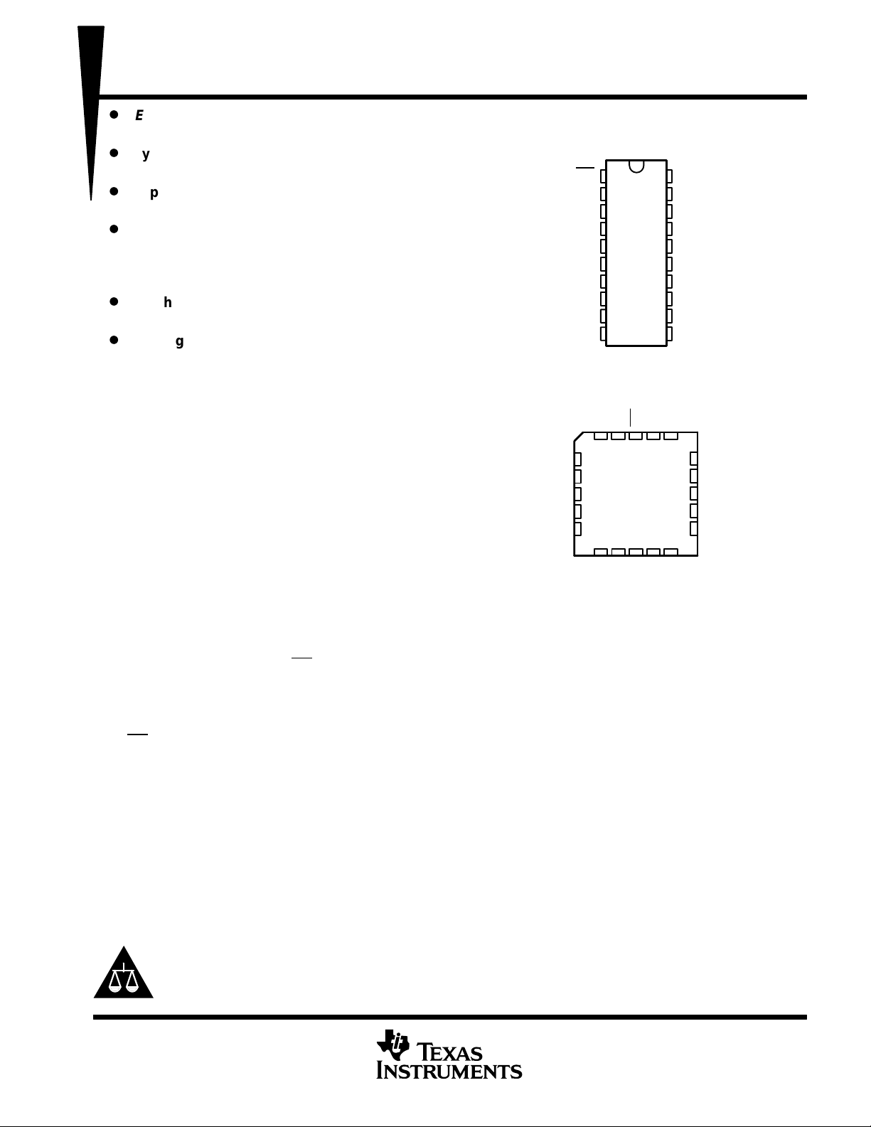
SN54LV573...J OR W PACKAGE
SN74LV573. . . DB, DW, OR PW PACKAGE
SN54LV573. . . FK PACKAGE
3D
4D
5D
6D
7D
(TOP VIEW)
OE
1
1D
2
2D
3
3D
4
4D
5
5D
6
6D
7
7D
8
8D
9
GND
10
(TOP VIEW)
2D1DOE
3212019
4
5
6
7
8
910111213
8D
GND
LE
20
19
18
17
16
15
14
13
12
11
CC
V
8Q
V
1Q
2Q
3Q
4Q
5Q
6Q
7Q
8Q
LE
1Q
18
17
16
15
14
7Q
CC
2Q
3Q
4Q
5Q
6Q
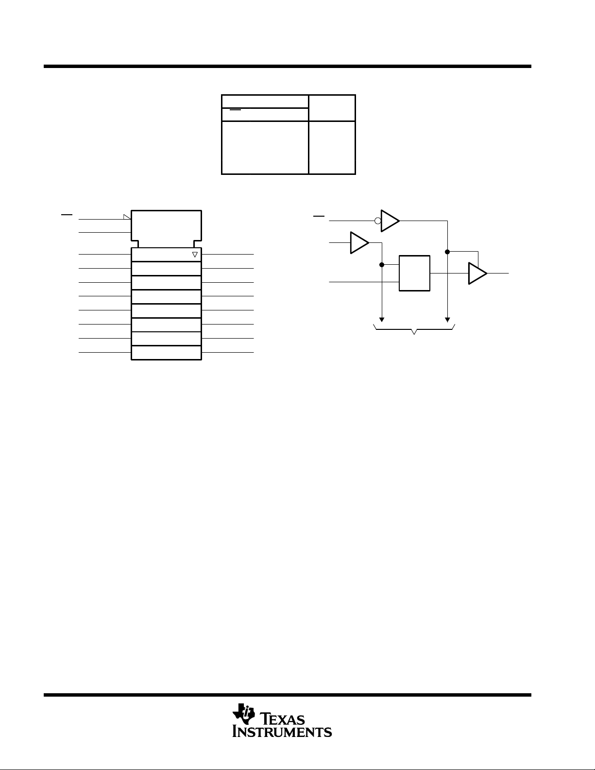
While the latch-enable (LE) input is high, the Q outputs follow the data (D) inputs. When LE is taken low, the
Q outputs are latched at the logic levels set up at the D inputs.
A buffered output-enable (OE
) input can be used to place the eight outputs in either a normal logic state (high
or low logic levels) or high-impedance state. In the high-impedance state, the outputs neither load nor drive the
bus lines significantly . The high-impedance state and increased drive provide the capability to drive bus lines
without need for interface or pullup components.
OE
does not affect the internal operations of the latches. Old data can be retained or new data can be entered
while the outputs are in the high-impedance state.
The SN74L V573 is available in TI’s shrink small-outline package (DB), which provides the same I/O pin count
and functionality of standard small-outline packages in less than half the printed-circuit-board area.
The SN54L V573 is characterized for operation over the full military temperature range of –55°C to 125°C. The
SN74LV573 is characterized for operation from –40°C to 85°C.
Please be aware that an important notice concerning availability, standard warranty, and use in critical applications of
Texas Instruments semiconductor products and disclaimers thereto appears at the end of this data sheet.
EPIC is a trademark of Texas Instruments Incorporated.
UNLESS OTHERWISE NOTED this document contains PRODUCTION
DATA information current as of publication date. Products conform to
specifications per the terms of Texas Instruments standard warranty.
Production processing does not necessarily include testing of all
parameters.
Copyright 1996, Texas Instruments Incorporated
POST OFFICE BOX 655303 • DALLAS, TEXAS 75265
1
SN54LV573, SN74LV573
OUTPUT
OCTAL TRANSPARENT D-TYPE LATCHES
WITH 3-STATE OUTPUTS
SCLS198B – FEBRUARY 1993 – REVISED APRIL 1996
FUNCTION TABLE
(each latch)
INPUTS
OE LE D
L H H H
L HL L
LLX Q
HXX Z
OUTPUT
Q
0
logic symbol
OE
LE
1D
2D
3D
4D
5D
6D
7D
8D
†
This symbol is in accordance with ANSI/IEEE Std 91-1984 and
IEC Publication 617-12.
Pin numbers shown are for DB, DW, J, PW, and W packages.
†
1
11
2
3
4
5
6
7
8
9
EN
C1
1D
19
18
17
16
15
14
13
12
logic diagram (positive logic)
1
OE
11
LE
1Q
2Q
3Q
4Q
5Q
6Q
7Q
8Q
1D
2
To Seven Other Channels
C1
1D
19
1Q
absolute maximum ratings over operating free-air temperature range (unless otherwise noted)
Supply voltage range, V
Input voltage range, V
Output voltage range, V
Input clamp current, I
Output clamp current, I
Continuous output current, I
Continuous current through V
Maximum power dissipation at T
Storage temperature range, T
‡
Stresses beyond those listed under “absolute maximum ratings” may cause permanent damage to the device. These are stress ratings only, and
functional operation of the device at these or any other conditions beyond those indicated under “recommended operating conditions” is not
implied. Exposure to absolute-maximum-rated conditions for extended periods may affect device reliability.
NOTES: 1. The input and output voltage ratings may be exceeded if the input and output current ratings are observed.
2. This value is limited to 7 V maximum.
3. The maximum package power dissipation is calculated using a junction temperature of 150°C and a board trace length of 750 mils.
–0.5 V to 7 V. . . . . . . . . . . . . . . . . . . . . . . . . . . . . . . . . . . . . . . . . . . . . . . . . . . . . . . . . .
CC
(see Note 1) –0.5 V to VCC + 0.5 V. . . . . . . . . . . . . . . . . . . . . . . . . . . . . . . . . . . . . . . . . .
I
(see Notes 1 and 2) –0.5 V to VCC + 0.5 V. . . . . . . . . . . . . . . . . . . . . . . . . . . . . . . . .
O
(VI < 0 or VI > VCC) ±20 mA. . . . . . . . . . . . . . . . . . . . . . . . . . . . . . . . . . . . . . . . . . . . . . . .
IK
(VO < 0 or VO > VCC) ±50 mA. . . . . . . . . . . . . . . . . . . . . . . . . . . . . . . . . . . . . . . . . . . .
OK
(VO = 0 to VCC) ±35 mA. . . . . . . . . . . . . . . . . . . . . . . . . . . . . . . . . . . . . . . . . . . . . .
O
or GND ±70 mA. . . . . . . . . . . . . . . . . . . . . . . . . . . . . . . . . . . . . . . . . . . . . . . . . . .
CC
= 55°C (in still air) (see Note 3):DB package 0.6 W. . . . . . . . . . . . . . . . . . .
A
DW package 1.6 W. . . . . . . . . . . . . . . . . .
PW package 0.7 W. . . . . . . . . . . . . . . . . . .
–65°C to 150°C. . . . . . . . . . . . . . . . . . . . . . . . . . . . . . . . . . . . . . . . . . . . . . . . . . .
stg
‡
2
POST OFFICE BOX 655303 • DALLAS, TEXAS 75265
UNIT
VIHHigh-l
V
VILL
V
V
IOHHigh-l
t
A
IOLL
t
A
PARAMETER
TEST CONDITIONS
†
UNIT
OH
OL
I
V
V
GND
A
I
V
V
GND
A
I
V
V
GND
I
0
A
C
V
V
GND
F
C
V
V
or GND
pF
SN54LV573, SN74LV573
OCTAL TRANSPARENT D-TYPE LATCHES
WITH 3-STATE OUTPUTS
SCLS198B – FEBRUARY 1993 – REVISED APRIL 1996
recommended operating conditions (see Note 4)
SN54LV573 SN74LV573
MIN MAX MIN MAX
V
CC
V
I
V
O
∆t/∆v Input transition rise or fall rate 0 100 0 100 ns/V
T
A
NOTE 4: Unused inputs must be held high or low to prevent them from floating.
Supply voltage 2.7 5.5 2.7 5.5 V
evel input voltage
ow-level input voltage
Input voltage 0 V
Output voltage 0 V
evel output curren
ow-level output curren
Operating free-air temperature –55 125 –40 85 °C
VCC = 2.7 V to 3.6 V 2 2
VCC = 4.5 V to 5.5 V
VCC = 2.7 V to 3.6 V 0.8 0.8
VCC = 4.5 V to 5.5 V
VCC = 2.7 V to 3.6 V –8 –8
VCC = 4.5 V to 5.5 V –16 –16
VCC = 2.7 V to 3.6 V 8 8
VCC = 4.5 V to 5.5 V 16 16
3.15 3.15
1.65 1.65
CC
CC
0 V
0 V
CC
CC
m
m
electrical characteristics over recommended operating free-air temperature range (unless otherwise noted)
V
CC
IOH = –100 µA MIN to MAX VCC–0.2 VCC–0.2
V
OH
V
OL
I
OZ
CC
n
I
CC
i
o
†
For conditions shown as MIN or MAX, use the appropriate values under recommended operating conditions.
IOH = – 8 mA 3 V 2.4 2.4
IOH = – 16 mA 4.5 V 3.6 3.6
IOL = 100 µA MIN to MAX 0.2 0.2
IOL = 8 mA 3 V 0.4 0.4
IOL = 16 mA 4.5 V 0.55 0.55
=
or
I
CC
=
=
=
=
CC
CC
CC
CC
or
or
or
,
O
I
One input at VCC – 0.6 V,
Other inputs at VCC or GND
I
O
=
O
3.6 V ±1 ±1
5.5 V ±1 ±1
3.6 V ±5 ±5
5.5 V ±5 ±5
3.6 V 20 20
5.5 V 20 20
3 V to 3.6 V 500 500 µA
3.3 V 2.5 2.5
5 V 3 3
3.3 V 7 7
5 V 10 10
SN54LV573 SN74LV573
MIN TYP MAX MIN TYP MAX
V
V
µ
µ
µ
p
PRODUCT PREVIEW information concerns products in the formative or
design phase of development. Characteristic data and other
specifications are design goals. Texas Instruments reserves the right to
change or discontinue these products without notice.
POST OFFICE BOX 655303 • DALLAS, TEXAS 75265
3
SN54LV573, SN74LV573
(INPUT)
(OUTPUT)
t
Q
ns
(INPUT)
(OUTPUT)
t
Q
ns
OCTAL TRANSPARENT D-TYPE LATCHES
WITH 3-STATE OUTPUTS
SCLS198B – FEBRUARY 1993 – REVISED APRIL 1996
timing requirements over recommended ranges of supply voltage and operating free-air temperature (unless otherwise noted)
SN54LV573
VCC = 5.5 V
± 0.5 V
MIN MAX MIN MAX MIN MAX
t
w
t
su
t
h
Pulse duration, LE high 9 12 14 ns
Setup time, data before LE↓
Hold time, data after LE↓ 4 6 6 ns
4 6 7 ns
timing requirements over recommended ranges of supply voltage and operating free-air temperature (unless otherwise noted)
VCC = 5.5 V
± 0.5 V
MIN MAX MIN MAX MIN MAX
t
w
t
su
t
h
Pulse duration, LE high 9 12 14 ns
Setup time, data before LE↓
Hold time, data after LE↓ 4 6 6 ns
4 6 7 ns
VCC = 3.3 V
± 0.3 V
SN74LV573
VCC = 3.3 V
± 0.3 V
VCC = 2.7 V
VCC = 2.7 V
UNIT
UNIT
switching characteristics over recommended operating free-air temperature range, CL = 50 pF
(unless otherwise noted) (see Figure 1)
SN54LV573
UNIT
PARAMETER
pd
t
en
t
dis
FROM
D
LE
OE
OE
TO
Q 11 18 16 22 28 ns
Q 15 21 21 28 29 ns
VCC = 5 V ± 0.5 V VCC = 3.3 V ± 0.3 V VCC = 2.7 V
MIN TYP MAX MIN TYP MAX MIN MAX
9 19 13 23 29
12 21 19 25 31
switching characteristics over recommended operating free-air temperature range, CL = 50 pF
(unless otherwise noted) (see Figure 1)
SN74LV573
UNIT
PARAMETER
pd
t
en
t
dis
FROM
D
LE
OE
OE
TO
Q 11 18 16 22 28 ns
Q 15 21 21 28 29 ns
VCC = 5 V ± 0.5 V VCC = 3.3 V ± 0.3 V VCC = 2.7 V
MIN TYP MAX MIN TYP MAX MIN MAX
9 19 13 23 29
12 21 19 25 31
PRODUCT PREVIEW information concerns products in the formative or
design phase of development. Characteristic data and other
specifications are design goals. Texas Instruments reserves the right to
change or discontinue these products without notice.
4
POST OFFICE BOX 655303 • DALLAS, TEXAS 75265
3.3 V
CpdPower dissipation capacitance per latch
C
MHz
pF
5 V
SN54LV573, SN74LV573
OCTAL TRANSPARENT D-TYPE LATCHES
WITH 3-STATE OUTPUTS
SCLS198B – FEBRUARY 1993 – REVISED APRIL 1996
operating characteristics, V
PARAMETER
= 3.3 V, T
CC
= 25°C
A
Outputs enabled
Outputs disabled
Outputs enabled
Outputs disabled
TEST CONDITIONS VCC TYP UNIT
30
= 50 pF,f = 10
L
14
36
16
POST OFFICE BOX 655303 • DALLAS, TEXAS 75265
5

SN54LV573, SN74LV573
OCTAL TRANSPARENT D-TYPE LATCHES
WITH 3-STATE OUTPUTS
SCLS198B – FEBRUARY 1993 – REVISED APRIL 1996
PARAMETER MEASUREMENT INFORMATION
V
z
From Output
Under Test
CL = 50 pF
(see Note A)
Input
1 kΩ
1 kΩ
LOAD CIRCUIT
t
w
V
m
S1
V
m
Open
GND
V
i
0 V
Timing Input
Data Input
t
PLH/tPHL
t
PLZ/tPZL
t
PHZ/tPZH
WAVEFORM
CONDITION
V
m
V
i
V
z
TEST S1
Open
V
GND
VCC = 4.5 V
to 5.5 V
0.5 × V
CC
V
CC
2 × V
CC
V
m
t
su
V
m
z
VCC = 2.7 V
to 3.6 V
1.5 V
2.7 V
6 V
t
h
V
i
0 V
V
i
V
m
0 V
VOLTAGE WAVEFORMS
PULSE DURATION
Input
t
PLH
Output
t
Output
NOTES: A. CL includes probe and jig capacitance.
PHL
INVERTING AND NONINVERTING OUTPUTS
B. Waveform 1 is for an output with internal conditions such that the output is low except when disabled by the output control.
Waveform 2 is for an output with internal conditions such that the output is high except when disabled by the output control.
C. All input pulses are supplied by generators having the following characteristics: PRR ≤ 10 MHz, ZO = 50 Ω, tr ≤ 2.5 ns, tf≤ 2.5 ns.
D. The outputs are measured one at a time with one transition per measurement.
E. t
PLZ
F. t
PZL
G. t
PLH
V
m
V
V
VOLTAGE WAVEFORMS
PROPAGATION DELAY TIMES
and t
and t
and t
are the same as t
PHZ
are the same as ten.
PZH
are the same as tpd.
PHL
V
m
t
PHL
m
m
V
V
dis
m
t
PLH
m
.
Figure 1. Load Circuit and Voltage Waveforms
V
0 V
V
V
V
V
i
OH
OL
OH
OL
Output
Control
Output
Waveform 1
S1 at V
(see Note B)
Output
Waveform 2
S1 at GND
(see Note B)
VOLTAGE WAVEFORMS
SETUP AND HOLD TIMES
V
m
t
PZL
t
PLZ
V
t
PHZ
V
m
m
z
t
PZH
VOLTAGE WAVEFORMS
ENABLE AND DISABLE TIMES
LOW- AND HIGH-LEVEL ENABLING
V
m
VOL + 0.3 V
VOH – 0.3 V
V
i
0 V
0.5 × V
V
OL
V
OH
[
0 V
z
6
POST OFFICE BOX 655303 • DALLAS, TEXAS 75265

IMPORTANT NOTICE
T exas Instruments (TI) reserves the right to make changes to its products or to discontinue any semiconductor
product or service without notice, and advises its customers to obtain the latest version of relevant information
to verify, before placing orders, that the information being relied on is current.
TI warrants performance of its semiconductor products and related software to the specifications applicable at
the time of sale in accordance with TI’s standard warranty. Testing and other quality control techniques are
utilized to the extent TI deems necessary to support this warranty. Specific testing of all parameters of each
device is not necessarily performed, except those mandated by government requirements.
Certain applications using semiconductor products may involve potential risks of death, personal injury, or
severe property or environmental damage (“Critical Applications”).
TI SEMICONDUCTOR PRODUCTS ARE NOT DESIGNED, INTENDED, AUTHORIZED, OR WARRANTED
TO BE SUITABLE FOR USE IN LIFE-SUPPORT APPLICATIONS, DEVICES OR SYSTEMS OR OTHER
CRITICAL APPLICATIONS.
Inclusion of TI products in such applications is understood to be fully at the risk of the customer. Use of TI
products in such applications requires the written approval of an appropriate TI officer . Questions concerning
potential risk applications should be directed to TI through a local SC sales office.
In order to minimize risks associated with the customer’s applications, adequate design and operating
safeguards should be provided by the customer to minimize inherent or procedural hazards.
TI assumes no liability for applications assistance, customer product design, software performance, or
infringement of patents or services described herein. Nor does TI warrant or represent that any license, either
express or implied, is granted under any patent right, copyright, mask work right, or other intellectual property
right of TI covering or relating to any combination, machine, or process in which such semiconductor products
or services might be or are used.
Copyright 1996, Texas Instruments Incorporated
 Loading...