

Datasheet SN74LV4053AD, SN74LV4053APWR, SN74LV4053ADBR, SN74LV4053ADGVR, SN74LV4053ADR Datasheet (Texas Instruments)
...
ON CHANNELS
SN54LV4053A, SN74LV4053A
TRIPLE 2-CHANNEL ANALOG MULTIPLEXERS/DEMULTIPLEXERS
SCLS430 – MA Y 1999
D
EPIC
(Enhanced-Performance Implanted
CMOS) Process
D
High On-Off Output-Voltage Ratio
D
Low Crosstalk Between Switches
D
Individual Switch Controls
D
Extremely Low Input Current
D
Latch-Up Performance Exceeds 250 mA Per
JESD 17
D
ESD Protection Exceeds 2000 V Per
MIL-STD-883, Method 3015; Exceeds 200 V
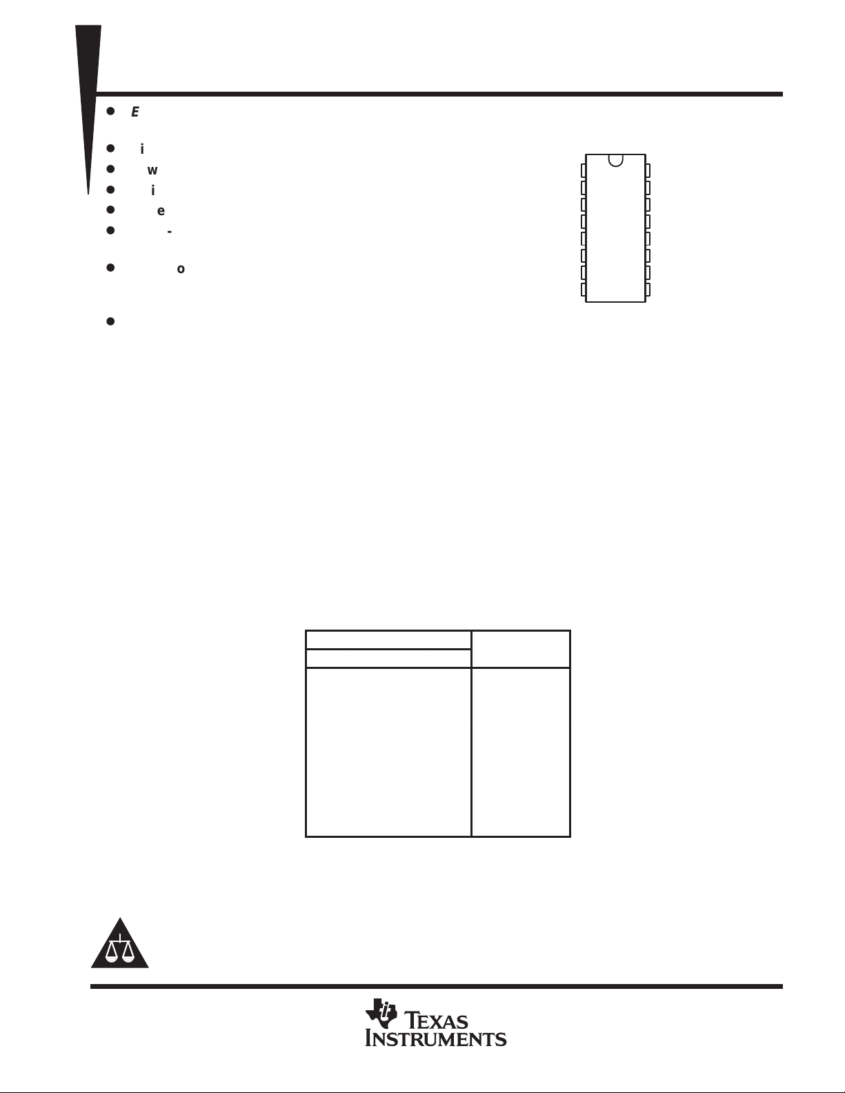
SN74LV4053A. . . D, DB, DGV, N, NS, OR PW PACKAGE
SN54LV4053A...J OR W PACKAGE
(TOP VIEW)
2Y1
2Y0
3Y1
3-COM
3Y0
INH
GND
GND
1
2
3
4
5
6
7
8
16
15
14
13
12
11
10
9
V
CC
2-COM
1-COM
1Y1
1Y0
A
B
C
Using Machine Model (C = 200 pF, R = 0)
D
Package Options Include Plastic
Small-Outline (D, NS), Shrink Small-Outline
(DB), Thin Very Small-Outline (DGV), Thin
Shrink Small-Outline (PW), Ceramic Flat
(W) Packages, and Standard Plastic (N) and
Ceramic (J) DIPs
description
These triple 2-channel CMOS analog multiplexers/demultiplexers are designed for 2-V to 5.5-V VCC operation.
The ’LV4053A devices handle both analog and digital signals. Each channel permits signals with amplitudes
up to 5.5 V (peak) to be transmitted in either direction.
Applications include signal gating, chopping, modulation or demodulation (modem), and signal multiplexing for
analog-to-digital and digital-to-analog conversion systems.
The SN54LV4053A is characterized for operation over the full military temperature range of –55°C to 125°C.
The SN74LV4053A is characterized for operation from –40°C to 85°C.
FUNCTION TABLE
INPUTS
INH C B A
L L L L 1Y0, 2Y0, 3Y0
L L L H 1Y1, 2Y0, 3Y0
L L H L 1Y0, 2Y1, 3Y0
L L H H 1Y1, 2Y1, 3Y0
L H L L 1Y0, 2Y0, 3Y1
L H L H 1Y1, 2Y0, 3Y1
L H H L 1Y0, 2Y1, 3Y1
L H H H 1Y1, 2Y1, 3Y1
H X X X None
Please be aware that an important notice concerning availability, standard warranty, and use in critical applications of
Texas Instruments semiconductor products and disclaimers thereto appears at the end of this data sheet.
EPIC is a trademark of Texas Instruments Incorporated.
UNLESS OTHERWISE NOTED this document contains PRODUCTION
DATA information current as of publication date. Products conform to
specifications per the terms of Texas Instruments standard warranty.
Production processing does not necessarily include testing of all
parameters.
POST OFFICE BOX 655303 • DALLAS, TEXAS 75265
Copyright 1999, Texas Instruments Incorporated
1
SN54LV4053A, SN74LV4053A
TRIPLE 2-CHANNEL ANALOG MULTIPLEXERS/DEMULTIPLEXERS
SCLS430 – MA Y 1999
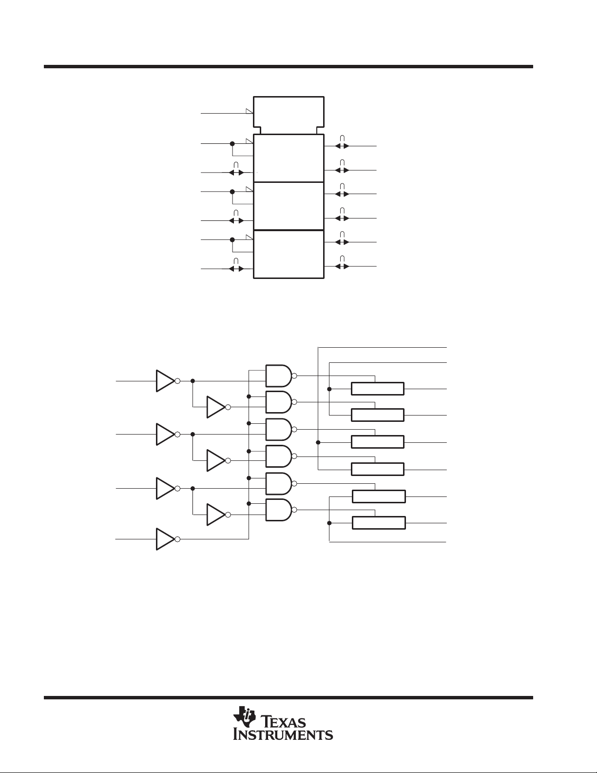
logic symbol
†
This symbol is in accordance with ANSI/IEEE Std 91-1984 and IEC Publication 617-12.
†
MUXDMUX
G2
2X0
2X1
0, 1
0
1
INH
1-COM
2-COM
3-COM
6
11
A
14
10
B
15
9
C
4
logic diagram (positive logic)
11
A
12
13
1Y0
1Y1
2
2Y0
1
2Y1
5
3Y0
3
3Y1
15
2-COM
14
1-COM
12
1Y0
INH
13
1Y1
10
B
9
C
6
2
1
5
3
4
2Y0
2Y1
3Y0
3Y1
3-COM
2
POST OFFICE BOX 655303 • DALLAS, TEXAS 75265
UNIT
VIHHigh-level input voltage, control inputs
V
VILLow-level input voltage, control inputs
V
SN54LV4053A, SN74LV4053A
TRIPLE 2-CHANNEL ANALOG MULTIPLEXERS/DEMULTIPLEXERS
SCLS430 – MA Y 1999
absolute maximum ratings over operating free-air temperature range (unless otherwise noted)
Supply voltage range, V
Input voltage range, V
Switch I/O voltage range, V
Input clamp current, I
I/O diode current, I
IOK
Switch through current, I
Continuous current through V
Package thermal impedance, θ
–0.5 V to 7.0 V. . . . . . . . . . . . . . . . . . . . . . . . . . . . . . . . . . . . . . . . . . . . . . . . . . . . . . . . .
CC
(see Note 1) –0.5 V to 7.0 V. . . . . . . . . . . . . . . . . . . . . . . . . . . . . . . . . . . . . . . . . . . . . . . . .
I
IK
(see Note 1 and Note 2) –0.5 V to VCC + 0.5 V. . . . . . . . . . . . . . . . . . . . . . . . . . .
IO
(V
< 0) –20 mA. . . . . . . . . . . . . . . . . . . . . . . . . . . . . . . . . . . . . . . . . . . . . . . . . . . . . . . . . . .
I
(VIO < 0 or VIO > VCC) ±50 mA. . . . . . . . . . . . . . . . . . . . . . . . . . . . . . . . . . . . . . . . . . . . . .
(V
= 0 to VCC) ±25 mA. . . . . . . . . . . . . . . . . . . . . . . . . . . . . . . . . . . . . . . . . . . . . . . . .
T
IO
or GND ±50 mA. . . . . . . . . . . . . . . . . . . . . . . . . . . . . . . . . . . . . . . . . . . . . . . . . . .
CC
(see Note 3): D package 113°C/W. . . . . . . . . . . . . . . . . . . . . . . . . . . . . . . . . .
JA
†
DB package 131°C/W. . . . . . . . . . . . . . . . . . . . . . . . . . . . . . . .
DGV package 180°C/W. . . . . . . . . . . . . . . . . . . . . . . . . . . . . . .
N package 78°C/W. . . . . . . . . . . . . . . . . . . . . . . . . . . . . . . . . . .
NS package 11 1°C/W. . . . . . . . . . . . . . . . . . . . . . . . . . . . . . . .
PW package 149°C/W. . . . . . . . . . . . . . . . . . . . . . . . . . . . . . . .
Storage temperature range, T
†
Stresses beyond those listed under “absolute maximum ratings” may cause permanent damage to the device. These are stress ratings only, and
functional operation of the device at these or any other conditions beyond those indicated under “recommended operating conditions” is not
implied. Exposure to absolute-maximum-rated conditions for extended periods may affect device reliability.
NOTES: 1. The input and output voltage ratings may be exceeded if the input and output clamp-current ratings are observed.
2. This value is limited to 7 V maximum.
3. The package thermal impedance is calculated in accordance with JESD 51, except for through-hole packages, which use a trace
length of zero.
–65°C to 150°C. . . . . . . . . . . . . . . . . . . . . . . . . . . . . . . . . . . . . . . . . . . . . . . . . . .
stg
recommended operating conditions (see Note 4)
SN74LV4053A SN74LV4053A
MIN MAX MIN MAX
V
V
V
∆t/∆v Input transition rise or fall rate
T
‡
With supply voltages at or near 2 V, the analog switch on-state resistance becomes very nonlinear . It is recommended that only digital signals
be transmitted at these low supply voltages.
NOTE 4: All unused control inputs of the device must be held at VCC or GND to ensure proper device operation. Refer to the TI application report,
Supply voltage 2
CC
VCC = 2 V 1.5 1.5
p
p
Control input voltage 0 5.5 0 5.5 V
I
Input/output voltage 0 V
IO
Operating free-air temperature –55 125 –40 85 °C
A
Implications of Slow or Floating CMOS Inputs
p
VCC = 2.3 V to 2.7 V VCC × 0.7 VCC × 0.7
p
VCC = 3 V to 3.6 V VCC × 0.7 VCC × 0.7
VCC = 4.5 V to 5.5 V VCC × 0.7 VCC × 0.7
VCC = 2 V 0.5 0.5
VCC = 2.3 V to 2.7 V VCC × 0.3 VCC × 0.3
VCC = 3 V to 3.6 V VCC × 0.3 VCC × 0.3
VCC = 4.5 V to 5.5 V VCC × 0.3 VCC × 0.3
VCC = 2.3 V to 2.7 V 0 200 0 200
VCC = 3 V to 3.6 V 0 100 0 100
VCC = 4.5 V to 5.5 V 0 20 0 20
, literature number SCBA004.
‡
5.5 2
CC
‡
0 V
5.5 V
CC
ns/V
V
PRODUCT PREVIEW information concerns products in the formative or
design phase of development. Characteristic data and other
specifications are design goals. Texas Instruments reserves the right to
change or discontinue these products without notice.
POST OFFICE BOX 655303 • DALLAS, TEXAS 75265
3
SN54LV4053A, SN74LV4053A
PARAMETER
V
UNIT
switch resistance
V
INH
V
IL
I
T
()
Difference in
I
T
TRIPLE 2-CHANNEL ANALOG MULTIPLEXERS/DEMULTIPLEXERS
SCLS430 – MA Y 1999
electrical characteristics over recommended operating free-air temperature range (unless
otherwise noted)
TA = 25°C SN54LV4053A SN74LV4053A
MIN TYP MAX MIN MAX MIN MAX
Ω
Ω
Ω
8.2 pF
5.6 pF
R
R
∆R
I
I
I
soff
I
son
I
CC
C
C
C
C
on
on(P)
on
IC
IS
OS
T
TEST
CONDITIONS
On-state
Peak on-state resistance
on-state resistance
between switches V
Control input current VI = VCC or GND 5.5 V ±0.1 ±1 ±1 µA
Off-state
switch leakage current
On-state
switch leakage current
Supply current VI = VCC or GND 5.5 V 20 20 µA
Control input capacitance 2 pF
Common
terminal capacitance
Switch
terminal capacitance
Feed-through capacitance 0.5 pF
IT = 2 mA,
VI = VCC or GND,
=
=
(see Figure 1)
=
= 2 mA,
VI = VCC to GND,
V
= V
INH
IL
=
= 2 mA,
VI = VCC to GND,
= V
INH
IL
VI = VCC and
VO = GND, or
VI = GND and
VO = VCC,
V
= V
INH
INH
= V
IH
IH
(see Figure 2)
VI = VCC or GND,
V
(see Figure 3)
CC
2.3 V 41 180 225 225
3 V 30 150 190 190
4.5 V 23 75 100 100
2.3 V 139 500 600 600
3 V 63 180 225 225
4.5 V 35 100 125 125
2.3 V 2 30 40 40
3 V 1.6 20 30 30
4.5 V 1.3 15 20 20
5.5 V ±0.1 ±1 ±1 µA
5.5 V ±0.1 ±1 ±1 µA
PRODUCT PREVIEW information concerns products in the formative or
design phase of development. Characteristic data and other
specifications are design goals. Texas Instruments reserves the right to
change or discontinue these products without notice.
4
POST OFFICE BOX 655303 • DALLAS, TEXAS 75265

PARAMETER
UNIT
PARAMETER
UNIT
SN54LV4053A, SN74LV4053A
TRIPLE 2-CHANNEL ANALOG MULTIPLEXERS/DEMULTIPLEXERS
switching characteristics over recommended operating free-air temperature range,
= 2.5 V ± 0.2 V (unless otherwise noted)
V
CC
FROM TO TEST
(INPUT) (OUTPUT) CONDITIONS
t
,
PLH
t
PHL
t
PZH
t
PZL
t
PHZ
t
PLZ
t
PLH
t
PHL
t
PZH
t
PZL
t
PHZ
t
PLZ
Propagation
delay time
,
Enable
delay time
,
Disable
delay time
,
Propagation
delay time
,
Enable
delay time
,
Disable
delay time
COM or
Yn
INH
INH
COM or
Yn
INH
INH
Yn or
COM
COM or
Yn
COM or
Yn
Yn or
COM
COM or
Yn
COM or
Yn
CL = 15 pF,
(see Figure 4)
CL = 15 pF,
(see Figure 5)
CL = 15 pF,
(see Figure 5)
CL = 50 pF,
(see Figure 4)
CL = 50 pF,
(see Figure 5)
CL = 50 pF,
(see Figure 5)
switching characteristics over recommended operating free-air temperature range,
= 3.3 V ± 0.3 V (unless otherwise noted)
V
CC
FROM TO TEST
(INPUT) (OUTPUT) CONDITIONS
t
,
PLH
t
PHL
t
PZH
t
PZL
t
PHZ
t
PLZ
t
PLH
t
PHL
t
PZH
t
PZL
t
PHZ
t
PLZ
Propagation
delay time
,
Enable
delay time
,
Disable
delay time
,
Propagation
delay time
,
Enable
delay time
,
Disable
delay time
COM or
Yn
INH
INH
COM or
Yn
INH
INH
Yn or
COM
COM or
Yn
COM or
Yn
Yn or
COM
COM or
Yn
COM or
Yn
CL = 15 pF,
(see Figure 4)
CL = 15 pF,
(see Figure 5)
CL = 15 pF,
(see Figure 5)
CL = 50 pF,
(see Figure 4)
CL = 50 pF,
(see Figure 5)
CL = 50 pF,
(see Figure 5)
TA = 25°C SN54LV4053A SN74LV4053A
MIN TYP MAX MIN MAX MIN MAX
2.5 10 16 16 ns
7.6 18 23 23 ns
7.7 18 23 23 ns
4.4 12 18 18 ns
8.8 28 35 35 ns
11.7 28 35 35 ns
TA = 25°C SN54LV4053A SN74LV4053A
MIN TYP MAX MIN MAX MIN MAX
1.6 6 10 10 ns
5.3 12 15 15 ns
6.1 12 15 15 ns
2.9 9 12 12 ns
6.1 20 25 25 ns
8.9 20 25 25 ns
SCLS430 – MA Y 1999
PRODUCT PREVIEW information concerns products in the formative or
design phase of development. Characteristic data and other
specifications are design goals. Texas Instruments reserves the right to
change or discontinue these products without notice.
POST OFFICE BOX 655303 • DALLAS, TEXAS 75265
5

SN54LV4053A, SN74LV4053A
PARAMETER
UNIT
PARAMETER
TEST CONDITIONS
V
UNIT
(switch on)
f
in
MHz (sine wave)
(between any switches)
f
in
MHz (sine wave)
(control in ut to signal out ut)
f
in
MHz (square wave)
(switch off)
f
in
MHz
R
(si
)
TRIPLE 2-CHANNEL ANALOG MULTIPLEXERS/DEMULTIPLEXERS
SCLS430 – MA Y 1999
switching characteristics over recommended operating free-air temperature range,
= 5 V ± 0.5 V (unless otherwise noted)
V
CC
FROM TO TEST
(INPUT) (OUTPUT) CONDITIONS
t
,
PLH
t
PHL
t
PZH
t
PZL
t
PHZ
t
PLZ
t
PLH
t
PHL
t
PZH
t
PZL
t
PHZ
t
PLZ
Propagation
delay time
,
Enable delay
time
,
Disable
delay time
,
Propagation
delay time
,
Enable delay
time
,
Disable
delay time
COM or
Yn
INH
INH
COM or
Yn
INH
INH
Yn or
COM
COM or
Yn
COM or
Yn
Yn or
COM
COM or
Yn
COM or
Yn
CL = 15 pF,
(see Figure 4)
CL = 15 pF,
(see Figure 5)
CL = 15 pF,
(see Figure 5)
CL = 50 pF,
(see Figure 4)
CL = 50 pF,
(see Figure 5)
CL = 50 pF,
(see Figure 5)
analog switch characteristics
FROM TO
(INPUT) (OUTPUT)
Frequency response
Crosstalk
Crosstalk
p
Feedthrough attenuation
Sine-wave distortion COM or Yn Yn or COM
NOTES: 5. Adjust fin voltage to obtain 0-dBm output. Increase fin frequency until dB meter reads –3 dB.
6. Adjust fin voltage to obtain 0-dBm input.
COM or Yn Yn or COM
COM or Yn Yn or COM
p
INH COM or Yn
COM or Yn Yn or COM
CL = 50 pF,
RL = 600 Ω,
=
= 1
(see Note 5 and Figure 6)
CL = 50 pF,
RL = 600 Ω,
= 1
(see Note 6 and Figure 7)
CL = 50 pF,
RL = 600 Ω,
= 1
(see Figure 8)
CL = 50 pF,
RL = 600 Ω,
= 1
(see Note 6 and Figure 9)
CL = 50 pF,
= 10 kΩ,
L
fin = 1 kHz
ne wave
(see Figure 10)
TA = 25°C SN54LV4053A SN74LV4053A
MIN TYP MAX MIN MAX MIN MAX
0.9 4 7 7 ns
3.8 8 10 10 ns
4.6 8 10 10 ns
1.8 6 8 8 ns
4.3 14 18 18 ns
6.3 14 18 18 ns
TA = 25°C
MIN TYP MAX
VI = 2 V
VI = 2.5 V
VI = 4 V
p-p
p-p
CC
2.3 V 30
3 V 35
4.5 V 50
2.3 V –45
3 V –45
4.5 V –45
2.3 V 20
3 V 35
4.5 V 65
2.3 V –45
3 V –45
4.5 V –45
2.3 V 0.1
p-p
3 V 0.1
4.5 V 0.1
MHz
dB
mV
dB
operating characteristics, VCC = 3.3 V, T
C
PRODUCT PREVIEW information concerns products in the formative or
design phase of development. Characteristic data and other
specifications are design goals. Texas Instruments reserves the right to
change or discontinue these products without notice.
6
Power dissipation capacitance f = 10 MHz 5.3 pF
pd
= 25°C
A
PARAMETER
POST OFFICE BOX 655303 • DALLAS, TEXAS 75265
TEST CONDITIONS TYP UNIT

SN54LV4053A, SN74LV4053A
TRIPLE 2-CHANNEL ANALOG MULTIPLEXERS/DEMULTIPLEXERS
SCLS430 – MA Y 1999
PARAMETER MEASUREMENT INFORMATION
V
CC
V
= V
INH
IL
V
CC
VI = VCC or GND
(ON)
GND
2 mA
V
VI – V
Figure 1. On-State Resistance Test Circuit
V
CC
V
= V
INH
IH
V
CC
V
I
A
(OFF)
GND
V
O
V
–V
I
2 10
O
W
–3
R
+
ON
O
V
O
Condition 1: VI = 0, VO = V
Condition 2: VI = VCC, VO = 0
CC
Figure 2. Off-State Switch Leakage-Current Test Circuit
V
CC
V
= V
INH
IL
V
CC
V
I
A
(ON)
GND
VI = VCC or GND
Open
Figure 3. On-State Switch Leakage-Current Test Circuit
POST OFFICE BOX 655303 • DALLAS, TEXAS 75265
7

SN54LV4053A, SN74LV4053A
TRIPLE 2-CHANNEL ANALOG MULTIPLEXERS/DEMULTIPLEXERS
SCLS430 – MA Y 1999
PARAMETER MEASUREMENT INFORMATION
V
CC
V
= V
INH
IH
V
CC
Input Output
(ON)
50 Ω
GND
Figure 4. Propagation Delay Time, Signal Input to Signal Output
V
CC
50 Ω
S1 S2
V
V
INH
CC
0 V
V
V
I
INH
V
CC
GND
TEST CIRCUIT
50%
t
PZL
1 kΩ
V
O
C
L
C
L
TEST S1 S2
t
PLZ/tPZL
t
PHZ/tPZH
V
CC
0 V
t
PZH
50%
GND
V
CC
V
CC
GND
≈ V
CC
V
O
V
OL
V
V
INH
CC
0 V
≈ V
CC
V
O
V
OL
Figure 5. Switching Time (t
8
50%
(t
, t
PZL
PZH
50%
t
PLZ
VOL + 0.3 V
(t
, t
PLZ
PHZ
VOLTAGE WAVEFORMS
, t
PZL
POST OFFICE BOX 655303 • DALLAS, TEXAS 75265
PLZ,
t
PZH
V
OH
≈ 0 V
)
V
CC
0 V
t
PHZ
V
OH
≈ 0 V
)
, t
), Control to Signal Output
PHZ
50%
50%
VOH – 0.3 V

SN54LV4053A, SN74LV4053A
TRIPLE 2-CHANNEL ANALOG MULTIPLEXERS/DEMULTIPLEXERS
SCLS430 – MA Y 1999
PARAMETER MEASUREMENT INFORMATION
V
CC
V
= GND
INH
V
f
in
50 Ω
NOTE A: fin is a sine wave.
0.1 µF
Figure 6. Frequency Response (Switch On)
V
= GND
INH
f
in
50 Ω
0.1 µF
600 Ω
CC
(ON)
GND
V
CC
V
CC
(ON)
GND
VCC/2
R
V
O
R
L
L
C
L
V
O1
C
L
VCC/2
V
V
= V
INH
CC
f
in
600 Ω
CC
V
CC
(OFF)
GND
VCC/2
R
L
Figure 7. Crosstalk Between Any Two Switches
50 Ω
V
600 Ω
INH
V
CC
V
CC
GND
R
L
C
V
O2
C
L
V
O
L
VCC/2 VCC/2
Figure 8. Crosstalk Between Control Input and Switch Output
POST OFFICE BOX 655303 • DALLAS, TEXAS 75265
9

SN54LV4053A, SN74LV4053A
TRIPLE 2-CHANNEL ANALOG MULTIPLEXERS/DEMULTIPLEXERS
SCLS430 – MA Y 1999
PARAMETER MEASUREMENT INFORMATION
V
CC
V
= GND
INH
0.1 µF
f
in
50 Ω
600 Ω
VCC/2
V
CC
(OFF)
GND
VCC/2
V
O
R
L
C
L
Figure 9. Feed-Through Attenuation (Switch Off)
V
CC
V
= GND
INH
10 µF
f
in
600 Ω
V
CC
(ON)
GND
VCC/2
R
L
10 µF
C
L
V
O
Figure 10. Sine-Wave Distortion
10
POST OFFICE BOX 655303 • DALLAS, TEXAS 75265

IMPORTANT NOTICE
T exas Instruments and its subsidiaries (TI) reserve the right to make changes to their products or to discontinue
any product or service without notice, and advise customers to obtain the latest version of relevant information
to verify, before placing orders, that information being relied on is current and complete. All products are sold
subject to the terms and conditions of sale supplied at the time of order acknowledgement, including those
pertaining to warranty, patent infringement, and limitation of liability.
TI warrants performance of its semiconductor products to the specifications applicable at the time of sale in
accordance with TI’s standard warranty. Testing and other quality control techniques are utilized to the extent
TI deems necessary to support this warranty . Specific testing of all parameters of each device is not necessarily
performed, except those mandated by government requirements.
CERT AIN APPLICATIONS USING SEMICONDUCTOR PRODUCTS MAY INVOLVE POTENTIAL RISKS OF
DEATH, PERSONAL INJURY, OR SEVERE PROPERTY OR ENVIRONMENTAL DAMAGE (“CRITICAL
APPLICATIONS”). TI SEMICONDUCTOR PRODUCTS ARE NOT DESIGNED, AUTHORIZED, OR
WARRANTED TO BE SUITABLE FOR USE IN LIFE-SUPPORT DEVICES OR SYSTEMS OR OTHER
CRITICAL APPLICA TIONS. INCLUSION OF TI PRODUCTS IN SUCH APPLICATIONS IS UNDERST OOD TO
BE FULLY AT THE CUSTOMER’S RISK.
In order to minimize risks associated with the customer’s applications, adequate design and operating
safeguards must be provided by the customer to minimize inherent or procedural hazards.
TI assumes no liability for applications assistance or customer product design. TI does not warrant or represent
that any license, either express or implied, is granted under any patent right, copyright, mask work right, or other
intellectual property right of TI covering or relating to any combination, machine, or process in which such
semiconductor products or services might be or are used. TI’s publication of information regarding any third
party’s products or services does not constitute TI’s approval, warranty or endorsement thereof.
Copyright 1999, Texas Instruments Incorporated
 Loading...