

Texas Instruments SN74LV4052ADBR, SN74LV4052ADGVR, SN74LV4052ADR, SN74LV4052AN, SN74LV4052ANSR Datasheet
...
SN54LV4052A, SN74LV4052A
DUAL 4-CHANNEL ANALOG MULTIPLEXERS/DEMULTIPLEXERS
SCLS429 – MA Y 1999
D
Operating Range 2-V to 5.5-V V
D
EPIC
(Enhanced-Performance Implanted
CC
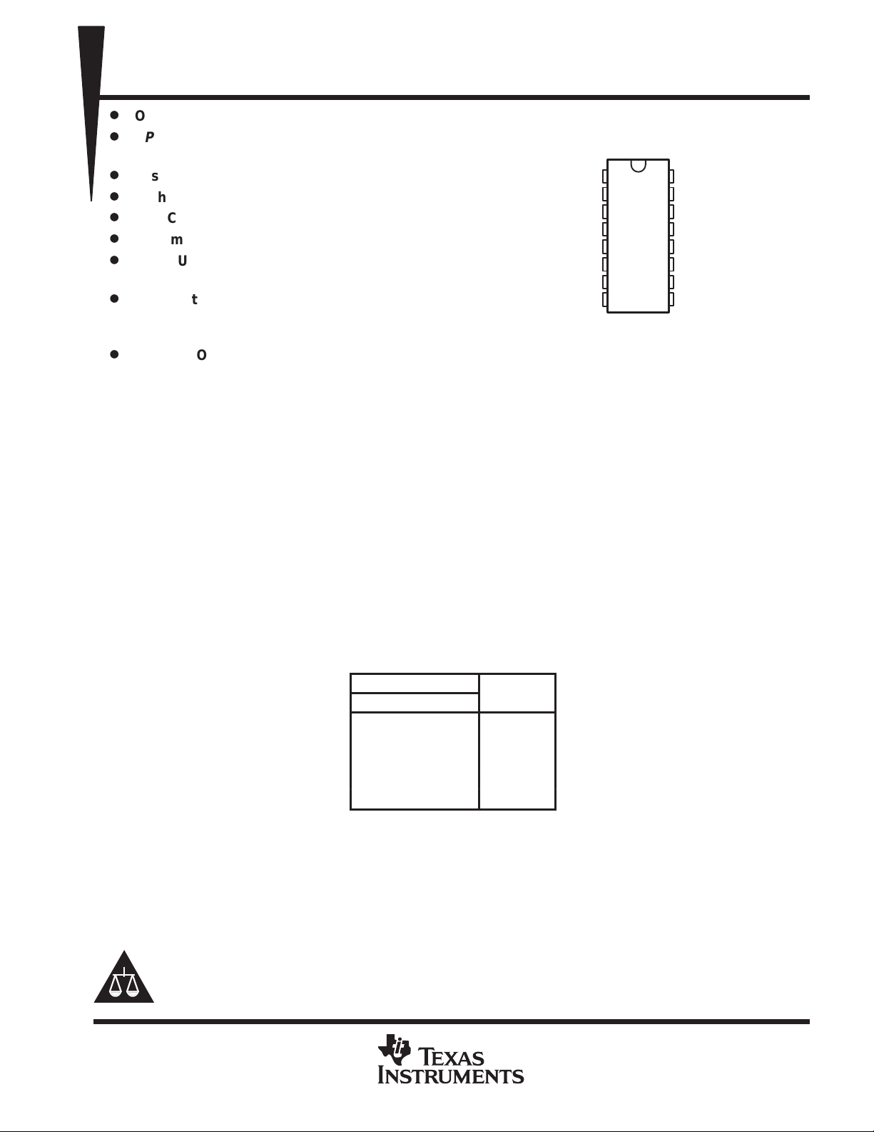
SN74LV4052A.. . D, DB, DGV, N, NS, OR PW PACKAGE
SN54LV4052A...J OR W PACKAGE
(TOP VIEW)
CMOS) Process
D
Fast Switching
D
High On-Off Output-Voltage Ratio
D
Low Crosstalk Between Switches
D
Extremely Low Input Current
D
Latch-Up Performance Exceeds 100 mA Per
JESD 78, Class II
D
ESD Protection Exceeds 2000 V Per
2Y0
2Y2
2-COM
2Y3
2Y1
INH
GND
GND
16
15
14
13
12
11
10
9
V
CC
1Y2
1Y1
1-COM
1Y0
1Y3
A
B
1
2
3
4
5
6
7
8
MIL-STD-883, Method 3015; Exceeds 200 V
Using Machine Model (C = 200 pF, R = 0)
D
Package Options Include Plastic
Small-Outline (D, NS), Shrink Small-Outline
(DB), Thin Very Small-Outline (DGV), Thin
Shrink Small-Outline (PW), Ceramic Flat
(W) Packages, and Plastic (N) and Ceramic
(J) DIPs
description
These dual 4-channel CMOS analog multiplexers/demultiplexers are designed for 2-V to 5.5-V VCC operation.
The ’LV4052A devices handle both analog and digital signals. Each channel permits signals with amplitudes
up to 5.5 V (peak) to be transmitted in either direction.
Applications include signal gating, chopping, modulation or demodulation (modem), and signal multiplexing for
analog-to-digital and digital-to-analog conversion systems.
The SN54LV4052A is characterized for operation over the full military temperature range of –55°C to 125°C.
The SN74LV4052A is characterized for operation from –40°C to 85°C.
FUNCTION TABLE
INPUTS
INH B A
L L L 1Y0, 2Y0
L L H 1Y1, 2Y1
L H L 1Y2, 2Y2
L H H 1Y3, 2Y3
H X X None
Please be aware that an important notice concerning availability, standard warranty, and use in critical applications of
Texas Instruments semiconductor products and disclaimers thereto appears at the end of this data sheet.
ON
CHANNEL
EPIC is a trademark of Texas Instruments Incorporated.
UNLESS OTHERWISE NOTED this document contains PRODUCTION
DATA information current as of publication date. Products conform to
specifications per the terms of Texas Instruments standard warranty.
Production processing does not necessarily include testing of all
parameters.
POST OFFICE BOX 655303 • DALLAS, TEXAS 75265
Copyright 1999, Texas Instruments Incorporated
1
SN54LV4052A, SN74LV4052A
DUAL 4-CHANNEL ANALOG MULTIPLEXERS/DEMULTIPLEXERS
SCLS429 – MA Y 1999
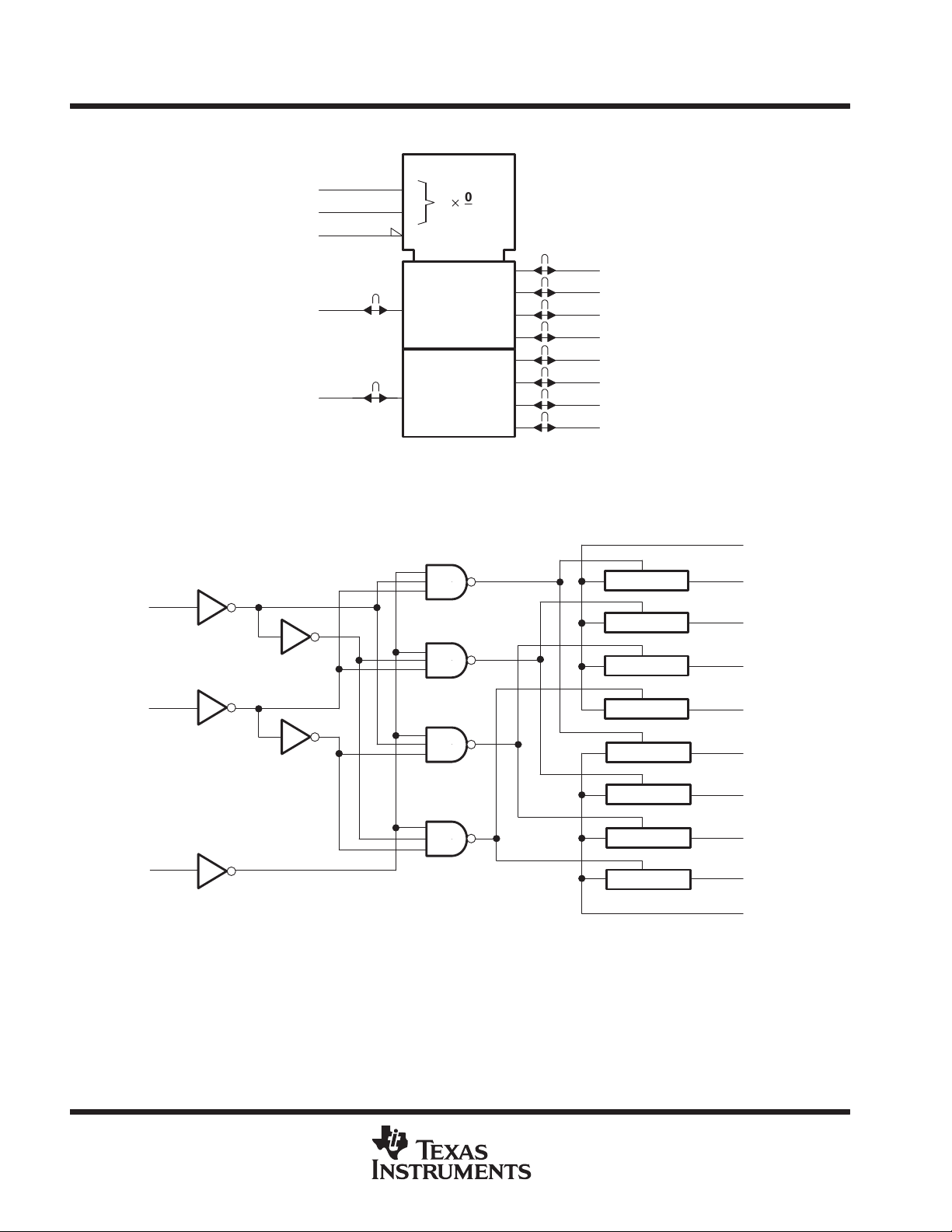
logic symbol
†
This symbol is in accordance with ANSI/IEEE Std 91-1984 and IEC Publication 617-12.
†
MUXDMUX
0
4
1
G4
0...3
0
3
0
1
2
3
INH
1-COM
2-COM
10
A
9
B
6
13
3
logic diagram (positive logic)
10
A
12
14
15
11
1Y0
1Y1
1Y2
1Y3
1
2Y0
5
2Y1
2
2Y2
4
2Y3
13
1-COM
12
1Y0
14
1Y1
INH
15
1Y2
9
B
6
11
1Y3
1
2Y0
5
2Y1
2
2Y2
4
2Y3
3
2-COM
2
POST OFFICE BOX 655303 • DALLAS, TEXAS 75265
UNIT
V
gg,
V
V
g,
V
SN54LV4052A, SN74LV4052A
DUAL 4-CHANNEL ANALOG MULTIPLEXERS/DEMULTIPLEXERS
SCLS429 – MA Y 1999
absolute maximum ratings over operating free-air temperature range (unless otherwise noted)
Supply voltage range, V
Input voltage range, V
Switch I/O voltage range, V
Input clamp current, I
I/O diode current, I
IOK
Switch through current, I
Continuous current through V
Package thermal impedance, θ
–0.5 V to 7.0 V. . . . . . . . . . . . . . . . . . . . . . . . . . . . . . . . . . . . . . . . . . . . . . . . . . . . . . . . .
CC
(see Note 1) –0.5 V to 7.0 V. . . . . . . . . . . . . . . . . . . . . . . . . . . . . . . . . . . . . . . . . . . . . . . . .
I
IK
(see Note 1 and Note 2) –0.5 V to VCC + 0.5 V. . . . . . . . . . . . . . . . . . . . . . . . . . .
IO
(V
< 0) –20 mA. . . . . . . . . . . . . . . . . . . . . . . . . . . . . . . . . . . . . . . . . . . . . . . . . . . . . . . . . . .
I
(VIO < 0 or VIO > VCC) ±50 mA. . . . . . . . . . . . . . . . . . . . . . . . . . . . . . . . . . . . . . . . . . . . . .
(V
= 0 to VCC) ±25 mA. . . . . . . . . . . . . . . . . . . . . . . . . . . . . . . . . . . . . . . . . . . . . . . . .
T
IO
or GND ±50 mA. . . . . . . . . . . . . . . . . . . . . . . . . . . . . . . . . . . . . . . . . . . . . . . . . . .
CC
(see Note 3): D package) 113°C/W. . . . . . . . . . . . . . . . . . . . . . . . . . . . . . . . .
JA
†
DB package) 131°C/W. . . . . . . . . . . . . . . . . . . . . . . . . . . . . . . .
DGV package) 180°C/W. . . . . . . . . . . . . . . . . . . . . . . . . . . . . .
N package) 78°C/W. . . . . . . . . . . . . . . . . . . . . . . . . . . . . . . . . .
NS package) 11 1 °C/W. . . . . . . . . . . . . . . . . . . . . . . . . . . . . . . .
PW package) 149°C/W. . . . . . . . . . . . . . . . . . . . . . . . . . . . . . .
Storage temperature range, T
†
Stresses beyond those listed under “absolute maximum ratings” may cause permanent damage to the device. These are stress ratings only, and
functional operation of the device at these or any other conditions beyond those indicated under “recommended operating conditions” is not
implied. Exposure to absolute-maximum-rated conditions for extended periods may affect device reliability.
NOTES: 1. The input and output voltage ratings may be exceeded if the input and output current ratings are observed.
2. This value is limited to 7 V maximum.
3. The package thermal impedance is calculated in accordance with JESD 51.
–65°C to 150°C. . . . . . . . . . . . . . . . . . . . . . . . . . . . . . . . . . . . . . . . . . . . . . . . . . .
stg
recommended operating conditions (see Note 4)
SN54LV4052A SN74LV4052A
MIN MAX MIN MAX
V
V
V
∆t/∆v Input transition rise or fall rate
T
‡
With supply voltages at or near 2 V, the analog switch on-state resistance becomes very nonlinear . It is recommended that only digital signals
be transmitted at these low supply voltages.
NOTE 4: All unused control inputs of the device must be held at VCC or GND to ensure proper device operation. Refer to the TI application report,
Supply voltage 2
CC
VCC = 2 V 1.5 1.5
High-level input voltage,
IH
control inputs
Low-level input voltage,
IL
control inputs
Control input voltage 0 5.5 0 5.5 V
I
Input/output voltage 0 V
IO
Operating free-air temperature –55 125 –40 85 °C
A
Implications of Slow or Floating CMOS Inputs
VCC = 2.3 V to 2.7 V
VCC = 3 V to 3.6 V
VCC = 4.5 V to 5.5 V VCC × 0.7 VCC × 0.7
VCC = 2 V 0.5 0.5
VCC = 2.3 V to 2.7 V
VCC = 3 V to 3.6 V
VCC = 4.5 V to 5.5 V VCC × 0.3 VCC × 0.3
VCC = 2.3 V to 2.7 V 0 200 0 200
VCC = 3 V to 3.6 V
VCC = 4.5 V to 5.5 V 0 20 0 20
, literature number SCBA004.
‡
VCC × 0.7 VCC × 0.7
VCC × 0.7 VCC × 0.7
0 100 0 100
5.5 2
VCC × 0.3 VCC × 0.3
VCC × 0.3 VCC × 0.3
CC
‡
0 V
5.5 V
CC
ns/V
V
PRODUCT PREVIEW information concerns products in the formative or
design phase of development. Characteristic data and other
specifications are design goals. Texas Instruments reserves the right to
change or discontinue these products without notice.
POST OFFICE BOX 655303 • DALLAS, TEXAS 75265
3

SN54LV4052A, SN74LV4052A
PARAMETER
TEST CONDITIONS
V
UNIT
switch resistance
V
INH
V
IL
I
T
()
on-state resistance
Difference in
I
T
DUAL 4-CHANNEL ANALOG MULTIPLEXERS/DEMULTIPLEXERS
SCLS429 – MA Y 1999
electrical characteristics over recommended operating free-air temperature range (unless
otherwise noted)
TA = 25°C SN54LV4052A SN74LV4052A
MIN TYP MAX MIN MAX MIN MAX
Ω
Ω
Ω
R
R
∆R
I
I
I
soff
I
son
I
CC
C
C
C
C
CC
On-state
on
Peak
on(p)
on
IC
IS
OS
T
-
on-state resistance
between switches V
Control input current VI = VCC or GND 5.5 V ±0.1 ±1 ±1 µA
Off-state switch
leakage current
On-state switch
leakage current
Supply current VI = VCC or GND 5.5 V 20 20 µA
Control input
capacitance
Common terminal
capacitance
Switch terminal
capacitance
Feed through
capacitance
IT = 2 mA,
VI = VCC or GND,
=
=
(see Figure 1)
=
= 2 mA,
VI = VCC to GND,
V
= V
INH
IL
=
= 2 mA,
VI = VCC to GND,
= V
INH
IL
VI = VCC and VO = GND, or
VI = GND and VO = VCC,
V
= V
INH
INH
= V
IH
IL
(see Figure 2)
VI = VCC or GND,
V
(see Figure 3)
f = 10 MHz 3.3 V 2.1 pF
2.3 V 43 180 225 225
3 V 34 150 190 190
4.5 V 25 75 100 100
2.3 V 133 500 600 600
3 V 63 180 225 225
4.5 V 35 100 125 125
2.3 V 1.5 30 40 40
3 V 1.1 20 30 30
4.5 V 0.7 15 20 20
5.5 V ±0.1 ±1 ±1 µA
5.5 V ±0.1 ±1 ±1 µA
3.3 V 13.1 pF
3.3 V 5.6 pF
3.3 V 0.5 pF
PRODUCT PREVIEW information concerns products in the formative or
design phase of development. Characteristic data and other
specifications are design goals. Texas Instruments reserves the right to
change or discontinue these products without notice.
4
POST OFFICE BOX 655303 • DALLAS, TEXAS 75265
 Loading...