

Texas Instruments SN74LV367AD, SN74LV367ADBR, SN74LV367ADGVR, SN74LV367ADR, SN74LV367ANSR Datasheet
...
SN54LV367A, SN74LV367A
HEX BUFFERS AND LINE DRIVERS
WITH 3-STATE OUTPUTS
SCLS398B – APRIL 1998 – REVISED SEPTEMBER 1999
D
EPIC
(Enhanced-Performance Implanted
CMOS) Process
D
Typical V
(Output Ground Bounce)
OLP
< 0.8 V at VCC = 3.3 V, TA = 25°C
D
Typical V
> 2 V at V
D
Latch-Up Performance Exceeds 100 mA Per
(Output VOH Undershoot)
OHV
= 3.3 V, TA = 25°C
CC
JESD 78, Class II
D
ESD Protection Exceeds JESD-22
– 2000-V Human-Body Model (A114-A)
– 200-V Machine Model (A115-A)
– 1000-V Charged-Device Model (C101)
D
Package Options Include Plastic
Small-Outline (D, NS), Shrink Small-Outline
(DB), Thin Very Small-Outline (DGV), and
Thin Shrink Small-Outline (PW) Packages,
Ceramic Flat (W) Packages, Chip Carriers
(FK), and DIPs (J)
description
The ’LV367A devices are hex buffers and line
drivers designed for 2-V to 5.5-V VCC operation.
These devices are designed specifically to
improve both the performance and density of
3-state memory address drivers, clock drivers,
and bus-oriented receivers and transmitters.
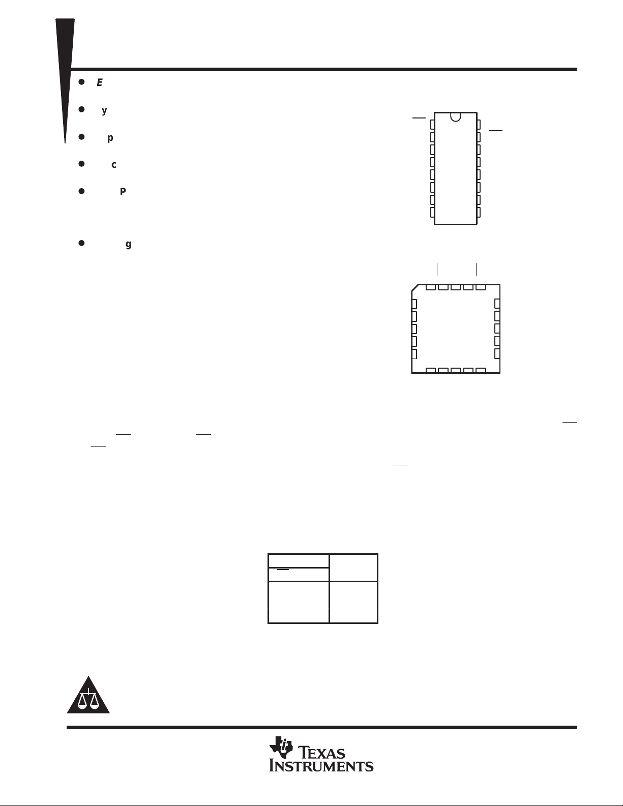
SN74LV367A. . . D, DB, DGV, NS, OR PW PACKAGE
SN54LV367A...J OR W PACKAGE
(TOP VIEW)
NC
NC
16
15
14
13
12
11
10
9
CC
V
1Y4
V
CC
2OE
2A2
2Y2
2A1
2Y1
1A4
1Y4
2OE
18
17
16
15
14
1A4
2A2
2Y2
NC
2A1
2Y1
1OE
1
1A1
2
1Y1
3
1A2
4
5
1Y2
6
1A3
7
1Y3
GND
SN54LV367A. . . FK PACKAGE
1Y1
1A2
NC
1Y2
1A3
NC – No internal connection
8
(TOP VIEW)
1A1
1OE
3212019
4
5
6
7
8
910111213
1Y3
GND
The ’L V367A devices are organized as dual 4-line and 2-line buffers/drivers with active-low output-enable (1OE
and 2OE) inputs. When OE is low, the device passes noninverted data from the A inputs to the Y outputs. When
OE is high, the outputs are in the high-impedance state.
T o ensure the high-impedance state during power up or power down, OE should be tied to V
through a pullup
CC
resistor; the minimum value of the resistor is determined by the current-sinking capability of the driver.
The SN54L V367A is characterized for operation over the full military temperature range of –55°C to 125°C. The
SN74LV367A is characterized for operation from –40°C to 85°C.
FUNCTION TABLE
(each buffer/driver)
Please be aware that an important notice concerning availability, standard warranty, and use in critical applications of
Texas Instruments semiconductor products and disclaimers thereto appears at the end of this data sheet.
EPIC is a trademark of Texas Instruments Incorporated.
UNLESS OTHERWISE NOTED this document contains PRODUCTION
DATA information current as of publication date. Products conform to
specifications per the terms of Texas Instruments standard warranty.
Production processing does not necessarily include testing of all
parameters.
INPUTS
OE A
L H H
L LL
H X Z
OUTPUT
Y
Copyright 1999, Texas Instruments Incorporated
POST OFFICE BOX 655303 • DALLAS, TEXAS 75265
1
SN54LV367A, SN74LV367A
HEX BUFFERS AND LINE DRIVERS
WITH 3-STATE OUTPUTS
SCLS398B – APRIL 1998 – REVISED SEPTEMBER 1999
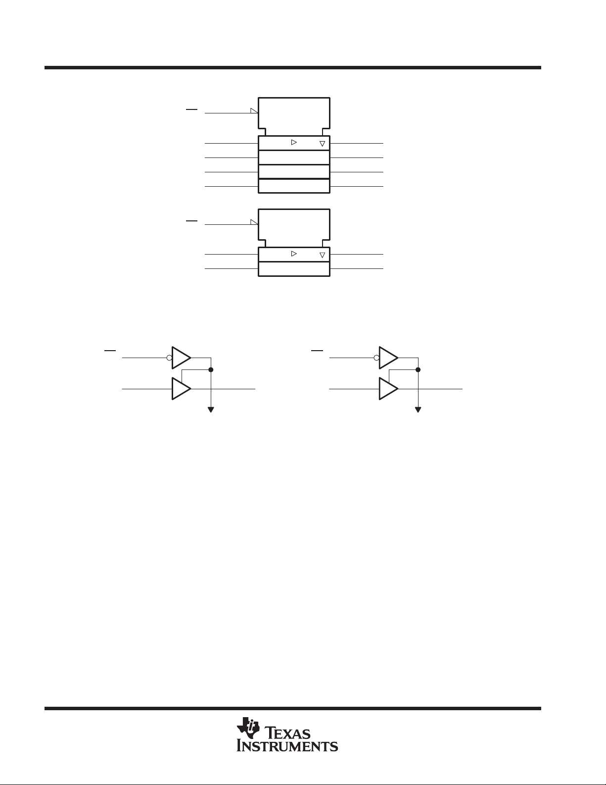
logic symbol
†
This symbol is in accordance with ANSI/IEEE Std 91-1984 and IEC Publication 617-12.
Pin numbers shown are for the D, DB, DGV, J, NS, PW, and W packages.
†
1OE
1A1
1A2
1A3
1A4
2OE
2A1
2A2
1
2
4
6
10
15
12
14
EN
EN
logic diagram (positive logic)
1OE
1
2OE
15
11
13
3
1Y1
5
1Y2
7
1Y3
9
1Y4
2Y1
2Y2
23
1A1
To Three Other Channels
Pin numbers shown are for the D, DB, DGV, J, NS, PW, and W packages.
1Y1
12 11
2A1
To One Other Channel
2Y1
2
POST OFFICE BOX 655303 • DALLAS, TEXAS 75265
SN54LV367A, SN74LV367A
HEX BUFFERS AND LINE DRIVERS
WITH 3-STATE OUTPUTS
SCLS398B – APRIL 1998 – REVISED SEPTEMBER 1999
absolute maximum ratings over operating free-air temperature range (unless otherwise noted)
Supply voltage range, VCC –0.5 V to 7 V. . . . . . . . . . . . . . . . . . . . . . . . . . . . . . . . . . . . . . . . . . . . . . . . . . . . . . . . . .
Input voltage range, VI (see Note 1) –0.5 V to 7 V. . . . . . . . . . . . . . . . . . . . . . . . . . . . . . . . . . . . . . . . . . . . . . . . . .
Output voltage range applied in the high or low state, V
Output voltage range applied in high-impedance or power-off state, VO (see Note 1) –0.5 V to 7 V. . . . . . .
Input clamp current, IIK (VI < 0) –20 mA. . . . . . . . . . . . . . . . . . . . . . . . . . . . . . . . . . . . . . . . . . . . . . . . . . . . . . . . . . .
Output clamp current, IOK (VO < 0 or VO > VCC) ±50 mA. . . . . . . . . . . . . . . . . . . . . . . . . . . . . . . . . . . . . . . . . . . .
Continuous output current, IO (VO = 0 to VCC) ±35 mA. . . . . . . . . . . . . . . . . . . . . . . . . . . . . . . . . . . . . . . . . . . . . .
Continuous current through V
or GND ±70 mA. . . . . . . . . . . . . . . . . . . . . . . . . . . . . . . . . . . . . . . . . . . . . . . . . . .
CC
Package thermal impedance, θJA (see Note 3): D package 73°C/W. . . . . . . . . . . . . . . . . . . . . . . . . . . . . . . . . . .
DB package 82°C/W. . . . . . . . . . . . . . . . . . . . . . . . . . . . . . . . .
DGV package 120°C/W. . . . . . . . . . . . . . . . . . . . . . . . . . . . . . .
NS package 64°C/W. . . . . . . . . . . . . . . . . . . . . . . . . . . . . . . . .
PW package 108°C/W. . . . . . . . . . . . . . . . . . . . . . . . . . . . . . . .
Storage temperature range, T
†
Stresses beyond those listed under “absolute maximum ratings” may cause permanent damage to the device. These are stress ratings only, and
functional operation of the device at these or any other conditions beyond those indicated under “recommended operating conditions” is not
implied. Exposure to absolute-maximum-rated conditions for extended periods may affect device reliability.
NOTES: 1. The input and output voltage ratings may be exceeded if the input and output current ratings are observed.
2. This value is limited to 7 V maximum.
3. The package thermal impedance is calculated in accordance with JESD 51.
–65°C to 150°C. . . . . . . . . . . . . . . . . . . . . . . . . . . . . . . . . . . . . . . . . . . . . . . . . . .
stg
(see Notes 1 and 2) –0.5 V to VCC + 0.5 V. . . . . .
O
†
POST OFFICE BOX 655303 • DALLAS, TEXAS 75265
3
 Loading...