


SN74LV161284
19-BIT BUS INTERFACE
SCLS426A – OCTOBER 1998 – REVISED FEBRUARY 1999
D
1.4-kΩ Pullup Resistors Integrated on All
Open-Drain Outputs Eliminate the Need for
Discrete Resistors
D
Designed for the IEEE Std 1284-I (Level-1
Type) and IEEE Std 1284-II (Level-2 Type)
Electrical Specifications
D
Flow-Through Architecture Optimizes PCB
Layout
D
Latch-Up Performance Exceeds 250 mA Per
JEDEC 17
D
Package Options Include Plastic 300-mil
Shrink Small-Outline (DL) and Thin-Shrink
Small-Outline (DGG) Packages
description
The SN74LV161284 is designed for 4.5-V to
5.5-V V
asynchronous two-way communication between
data buses. The control-function implementation
minimizes external timing requirements.
This device has eight bidirectional bits; data can
flow in the A-to-B direction when DIR is high, and
in the B-to-A direction when DIR is low. This
device also has five drivers, which drive the cable
side, and four receivers. The SN74L V161284 has
one receiver dedicated to the HOST LOGIC line
and a driver to drive the PERI LOGIC line.
operation. This device provides
CC
DGG OR DL PACKAGE
HD
A9
A10
A1 1
A12
A13
V
CC
A1
A2
GND
A3
A4
A5
A6
GND
A7
A8
V
PERI LOGIC IN
HOST LOGIC OUT
CC
A14
A15
A16
A17
(TOP VIEW)
1
48
2
47
3
46
4
45
5
44
6
43
7
42
8
41
9
40
10
39
11
38
12
37
13
36
14
35
15
34
16
33
17
32
18
31
19
30
20
29
21
28
22
27
23
26
24
25
DIR
Y9
Y10
Y11
Y12
Y13
CABLE
V
CC
B1
B2
GND
B3
B4
B5
B6
GND
B7
B8
CABLE
V
CC
PERI LOGIC OUT
C14
C15
C16
C17
HOST LOGIC IN
The output drive mode is determined by the high-drive (HD) control pin. When HD is high, the B, Y, and PERI
LOGIC OUT outputs are in a totem-pole configuration, and in an open-drain configuration when HD is low. This
meets the drive requirements as specified in the IEEE Std 1284-I (level-1 type) and IEEE Std 1284-II (level-2
type) parallel peripheral-interface specifications. Except for HOST LOGIC IN and PERI LOGIC OUT, all
cable-side pins have a 1.4-kΩ integrated pullup resistor. The pullup resistor is switched off if the associated
output driver is in the low state or if the output voltage is above V
CABLE. If VCC CABLE is off, PERI LOGIC
CC
OUT is set to low.
The device has two supply voltages. V
is designed for 4.5-V to 5.5-V operation. VCC CABLE supplies the
CC
output buffers of the cable side only and is designed for 4.5-V to 5.5-V operation.
The SN74LV161284 is characterized for operation from –40°C to 85°C.
Please be aware that an important notice concerning availability, standard warranty, and use in critical applications of
Texas Instruments semiconductor products and disclaimers thereto appears at the end of this data sheet.
PRODUCTION DATA information is current as of publication date.
Products conform to specifications per the terms of Texas Instruments
standard warranty. Production processing does not necessarily include
testing of all parameters.
Copyright 1999, Texas Instruments Incorporated
POST OFFICE BOX 655303 • DALLAS, TEXAS 75265
1
SN74LV161284
OUTPUT
MODE
L
L
H
L
19-BIT BUS INTERFACE
SCLS426A – OCTOBER 1998 – REVISED FEBRUARY 1999
FUNCTION TABLE
INPUTS
DIR
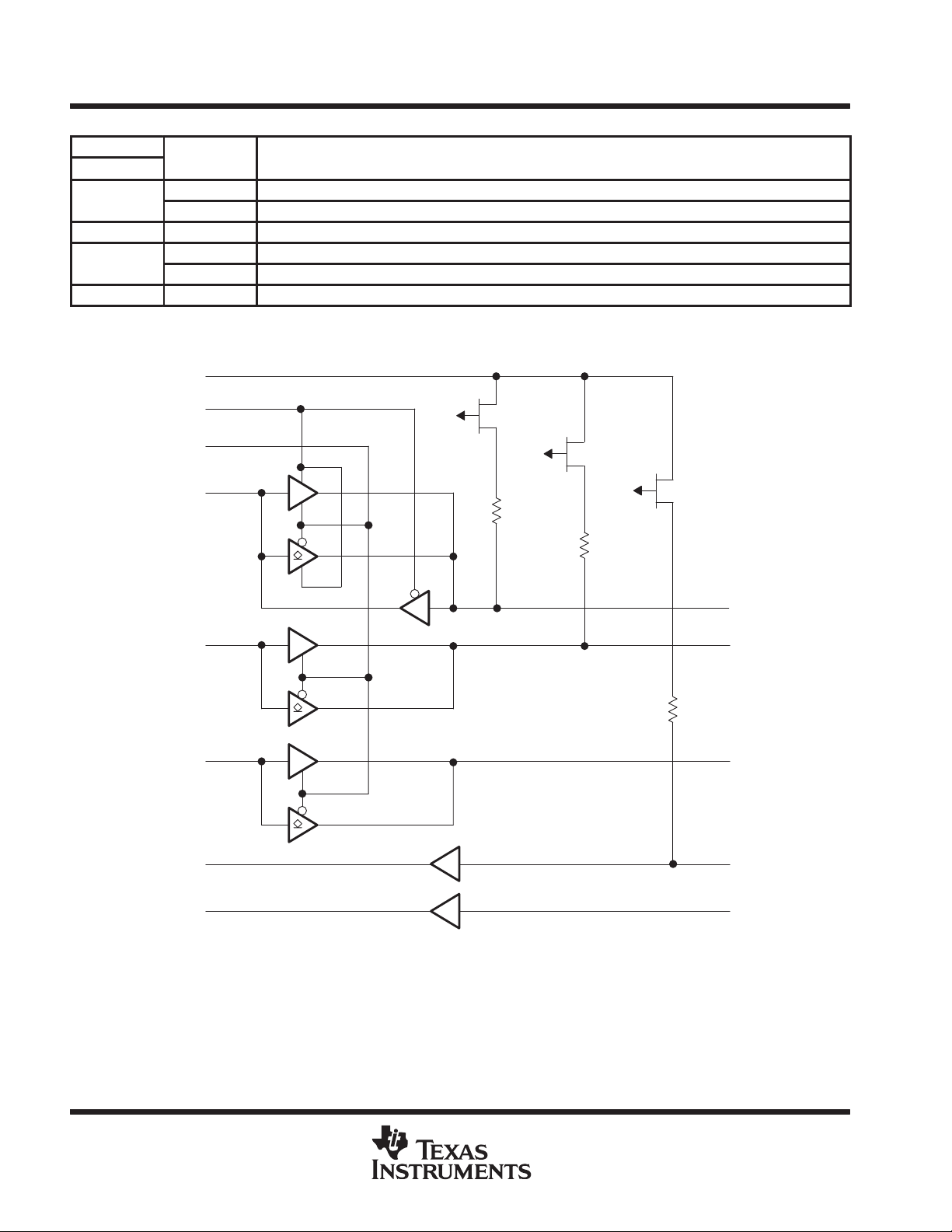
logic diagram (positive logic)
HD
Open drain A9–A13 to Y9–Y13 and PERI LOGIC IN to PERI LOGIC OUT
Totem pole B1–B8 to A1–A8 and C14–C17 to A14–A17
L H Totem pole B1–B8 to A1–A8, A9–A13 to Y9–Y13, PERI LOGIC IN to PERI LOGIC OUT , and C14–C17 to A14–A17
Open drain A1–A8 to B1–B8, A9–A13 to Y9–Y13, and PERI LOGIC IN to PERI LOGIC OUT
Totem pole C14–C17 to A14–A17
H H Totem pole A1–A8 to B1–B8, A9–A13 to Y9–Y13, C14–C17 to A14–A17, and PERI LOGIC IN to PERI LOGIC OUT
VCC CABLE
DIR
HD
A1–A8
A9–A13
PERI LOGIC IN
42
48
1
19
See Note B
See Note B
See Note A
B1–B8
Y9–Y13
30
PERI LOGIC OUT
A14–A17
HOST LOGIC OUT
NOTES: A. The PMOS prevents backdriving current from the signal pins to VCC CABLE when VCC CABLE is open or at GND.
B. The PMOS prevents backdriving current from the signal pins to VCC CABLE when VCC CABLE is open or at GND. The PMOS
is turned off when the associated driver is in the low state.
2
24
POST OFFICE BOX 655303 • DALLAS, TEXAS 75265
C14–C17
25
HOST LOGIC IN
VIHHigh-level input voltage
V
VILLow-level input voltage
V
VIInput voltage
V
SN74LV161284
19-BIT BUS INTERFACE
SCLS426A – OCTOBER 1998 – REVISED FEBRUARY 1999
absolute maximum ratings over operating free-air temperature range (unless otherwise noted)
Supply voltage range: V
Input and output voltage range, V
Input clamp current, I
Output clamp current, I
Continuous output current, I
Continuous current through each V
Output high sink current, I
Package thermal impedance, θ
CABLE –0.5 V to 7 V. . . . . . . . . . . . . . . . . . . . . . . . . . . . . . . . . . . . . . . . . . . . . . . . . .
CC
V
–0.5 V to 7 V. . . . . . . . . . . . . . . . . . . . . . . . . . . . . . . . . . . . . . . . . . . . . . . . . . . . . . . . .
CC
and VO: Cable side (see Notes 1 and 2) –2 V to 7 V. . . . . . . . . . . . . . . . . .
I
Peripheral side (see Note 1) –0.5 V to V
(VI < 0 or VI > VCC ) ±20 mA. . . . . . . . . . . . . . . . . . . . . . . . . . . . . . . . . . . . . . . . . . . . . . .
IK
(VO < 0 or VO > VCC) ±50 mA. . . . . . . . . . . . . . . . . . . . . . . . . . . . . . . . . . . . . . . . . . . .
OK
(VO = 0 to VCC) ±50 mA. . . . . . . . . . . . . . . . . . . . . . . . . . . . . . . . . . . . . . . . . . . . . .
O
(VO = 5.5 V and VCC CABLE = 5.5 V) 65 mA. . . . . . . . . . . . . . . . . . . . . . . . . . . .
SK
JA
or GND ±200 mA. . . . . . . . . . . . . . . . . . . . . . . . . . . . . . . . . . . . . . . . . . . . .
CC
(see Note 3): DGG package 89°C/W. . . . . . . . . . . . . . . . . . . . . . . . . . . . . . .
CC
†
+ 0.5 V. . . . . . . . . . .
DL package 94°C/W. . . . . . . . . . . . . . . . . . . . . . . . . . . . . . . . .
Storage temperature range, T
†
Stresses beyond those listed under “absolute maximum ratings” may cause permanent damage to the device. These are stress ratings only, and
functional operation of the device at these or any other conditions beyond those indicated under “recommended operating conditions” is not
implied. Exposure to absolute-maximum-rated conditions for extended periods may affect device reliability.
NOTES: 1. The input and output voltage ratings may be exceeded if the input and output current ratings are observed.
2. The ac input voltage pulse duration is limited to 40 ns if the amplitude is more negative than –0.5 V.
3. The package thermal impedance is calculated in accordance with JESD 51.
–65°C to 150°C. . . . . . . . . . . . . . . . . . . . . . . . . . . . . . . . . . . . . . . . . . . . . . . . . . .
stg
recommended operating conditions (see Note 4)
MIN MAX UNIT
VCC CABLE Supply voltage for the cable side, VCC CABLE ≥ V
V
CC
V
O
I
OH
I
OL
T
A
NOTE 4: All unused inputs of the device must be held at VCC or GND to ensure proper device operation. Refer to the TI application report,
Supply voltage 4.5 5.5 V
p
p
p
Open-drain output voltage B, Y, and PERI LOGIC OUT (HD low) 0 5.5 V
High-level output current
Low-level output current
Operating free-air temperature –40 85 °C
Implications of Slow or Floating CMOS Inputs
, literature number SCBA004.
CC
A, DIR, HD, and PERI LOGIC IN VCC × 0.7
B 2
C14–C17 2.3
HOST LOGIC IN 2.6
A, DIR, HD, and PERI LOGIC IN VCC × 0.3
B 0.8
C14–C17 0.8
HOST LOGIC IN 1.6
Peripheral side 0 V
Cable side 0 5.5
B and Y outputs (HD high) –14
A outputs and HOST LOGIC OUT
PERI LOGIC OUT –0.5
B and Y outputs 14
A outputs and HOST LOGIC OUT 8
PERI LOGIC OUT 84
4.5 5.5 V
CC
mA
–8
mA
POST OFFICE BOX 655303 • DALLAS, TEXAS 75265
3

SN74LV161284
5 V
VOHA outputs and HOST LOGIC OUT
V
VOLA outputs and HOST LOGIC OUT
4.5 V
V
C inputs
5.5 V
I
B outputs
I
I
B and Y outputs
0 to 2 V
I
B and Y outputs
2 V to 0
I
0
A
I
‡
5.5 V
mA
19-BIT BUS INTERFACE
SCLS426A – OCTOBER 1998 – REVISED FEBRUARY 1999
electrical characteristics over recommended operating free-air temperature range,
CABLE = VCC (unless otherwise noted)
V
CC
PARAMETER TEST CONDITIONS V
V
– V
thH
∆V
V
IK
I
OZ
OZPU
OZPD
off
CC
C
i
C
io
Z
O
R pullup Cable side VO = 0 V (in Hi Z) 5 V 1.15 1.65 kΩ
†
All typical values are at VCC = 5 V, TA = 25°C.
‡
A maximum current of 170 µA per pin is added to ICC if the pullup resistor pin is above VCC.
Input hysteresis
t
Input clamp diode voltage II = –18 mA 3 V –1.2 V
B and Y outputs IOH = –14 mA (HD high) 3.73
p
PERI LOGIC OUT IOH = –0.5 mA 4.5 V 4.45
B and Y outputs IOL = 14 mA 0.77
p
PERI LOGIC OUT IOL = 84 mA 0.7
p
B and C inputs VI = 5.5 V or GND 0 to 5.5 V ±5 mA
All inputs except the B or C inputs VI = VCC or GND 5.5 V ±1 µA
p
A1–A8 VO = VCC or GND 5.5 V ±20 µA
Open-drain Y outputs VO = GND (pullup resistors) 5.5 V –5 mA
p
p
Power-down output leakage,
Outputs B1 – B8, Y9 – Y13, and
PERI LOGIC OUT
Power-down input leakage,
Inputs C14 – C17 and HOST
LOGIC IN
All inputs VI = VCC or GND 5 V 5 pF
I/O ports VO = VCC or GND 5 V 9 pF
Cable side IOH = –35 mA 5 V 45 Ω
C inputs and HOST LOGIC IN
V
thH
V
thH
IOH = –8 mA (HD high)
IOH = –50 µA 4.4
IOL = 50 µA
IOL = 8 mA
VI = V
VI = GND (pullup resistors)
VO = V
VO = GND (pullup resistors) 5.5 V –5 mA
VO = 5.5 V
VO = GND
VO = 5.5 V
VO = GND
VO = 5.5 V
VI = 5.5 V
VI = VCC, IO = 0
VI = GND (12 × pullup)
for all inputs except the
thL
– V
for the HOST LOGIC IN
thL
– V
for the C inputs
thL
CC
CC
CC
4.5 V to 5.5 V 0.4
4.5 V
5.5 V 350 µA
MIN TYP†MAX UNIT
0.3
0.8
3.8
0.44
350 µA
350 µA
350 µA
100
100
V
0.1
–5 mA
–5 mA
–5 mA
µ
0.8
70
4
POST OFFICE BOX 655303 • DALLAS, TEXAS 75265

Totem pole
A or B
B or A
ns
Totem poleAY
ns
Totem poleCA
ns
Totem pole
PERI LOGIC IN
PERI LOGIC OUT
ns
Totem pole
HOST LOGIC IN
HOST LOGIC OUT
ns
t
DIR
ns
SN74LV161284
19-BIT BUS INTERFACE
SCLS426A – OCTOBER 1998 – REVISED FEBRUARY 1999
switching characteristics over recommended ranges of supply voltage and operating free-air
temperature (unless otherwise noted) (see Figures 1 and 2)
PARAMETER
t
PLH
t
PHL
t
PLH
t
PHL
t
PLH
t
PHL
t
PLH
t
PHL
t
PLH
t
PHL
t
slew
t
en
t
dis
ten–t
dis
t
en
dis
tr, t
f
t
sk(o)
†
Skew is measured at 1/2 (VOH + VOL) for signals switching in the same direction.
p
p
p
p
p
Totem pole Cable-side outputs 0.05 0.95 V/ns
Totem pole
Totem pole
Open drain
FROM
(INPUT)
HD
HD
DIR
A
A or B
B, Y, and PERI LOGIC OUT 2 25 ns
B, Y, and PERI LOGIC OUT 2 25 ns
TO
(OUTPUT)
A 2 25 ns
A 2 15
B 2 25
B or Y 30 ns
B or A 1 6 ns
MIN TYP MAX UNIT
2 30
2 30
2 30
2 30
2 30
2 30
2 30
2 30
2 30
2 30
10 ns
operating characteristics, V
C
Power dissipation capacitance Outputs enabled CL = 0, f = 10 MHz 25 pF
pd
= 5 V, T
CC
PARAMETER
= 25°C
A
TEST CONDITIONS TYP UNIT
POST OFFICE BOX 655303 • DALLAS, TEXAS 75265
5

SN74LV161284
19-BIT BUS INTERFACE
SCLS426A – OCTOBER 1998 – REVISED FEBRUARY 1999
PARAMETER MEASUREMENT INFORMATION
V
CC
62 Ω
CL = 50 pF
(see Note A)
Input
(see Note B)
t
w
VCC/2 VCC/2
V
0 V
CC
B or Y Output
From
Under Test
B or Y Output
TP1
From
62 Ω
Sink Load
t
PHL
t
PLH
Source Load
V
CC
TP1
t
PLH
Output
(see Note B)
CL = 50 pF
(see Note A)
SLEW RATE A-TO-B OR A-TO-Y LOAD (Totem Pole)
Input
(see Note C)
500 Ω
Output
CL = 50 pF
(see Note A)
(see Note C)
VOLTAGE WAVEFORMS MEASURED AT TP1
PROPAGATION DELAY TIMES (A to B)
VCC/2 VCC/2
2 V 2 V
0.8 V 0.8 V
VOLTAGE WAVEFORMS MEASURED AT TP1, B SIDE
VOL + 1.4 V
t
r
t
PHL
V
VOH – 1.4 V
V
V
0 V
V
V
t
f
OH
OL
CC
OH
OL
A-TO-B LOAD OR A-TO-Y LOAD (Open Drain)
NOTES: A. CL includes probe and jig capacitance.
B. Input rise and fall times are 3 ns, 150 ns < pulse duration < 10 µs for both low-to-high and high-to-low transitions.
Slew rate is measured between 0.4 V and 1.9 V for the rising edge and between 95% VCC and 50% VCC for the falling edge.
C. Input rise and fall times are 3 ns. Rise and fall times (open drain) < 120 ns.
D. The outputs are measured one at a time with one transition per measurement.
Figure 1. Load Circuits and Voltage Waveforms
6
POST OFFICE BOX 655303 • DALLAS, TEXAS 75265

From Output
Under Test
CL = 50 pF
(see Note A)
SCLS426A – OCTOBER 1998 – REVISED FEBRUARY 1999
PARAMETER MEASUREMENT INFORMATION
VCC × 2
500 Ω
500 Ω
S1
Open
GND
TEST S1
t
PLH/tPHL
t
PLZ/tPZL
t
PHZ/tPZH
SN74LV161284
19-BIT BUS INTERFACE
Open
VCC × 2
GND
Input
(see Note B)
t
PLH
Output
B or Y Output
Under Test
LOAD CIRCUIT
1.5 V 1.5 V
VCC/2
VOLTAGE WAVEFORMS
PROPAGATION DELAY TIMES (B to A)
V
CC
CL = 50 pF
(see Note A)
From
TP1
500 Ω
Sink Load
t
PHL
t
PLH
Source Load
3 V
0 V
t
PHL
V
VCC/2
V
B-TO-A LOAD (Totem Pole)
S1 at VCC × 2 V
OH
OL
Input
(see Note D)
Output
(see Note D)
Output
Control
Output
Waveform 1
(see Note C)
Output
Waveform 2
S1 at GND
(see Note C)
t
PLH
VCC/2
t
PZL
t
PLZ
VCC/2
t
t
PZH
ENABLE AND DISABLE TIMES
t
w
VCC/2 VCC/2
VOL + 1.4 V
PHZ
VCC/2
VOLTAGE WAVEFORMS
VCC/2
VOL + 0.3 V
VOH – 0.3 V
t
PHL
VOH – 1.4 V
V
0 V
V
V
CC
OH
OL
V
0 V
V
V
V
0 V
CC
CC
OL
OH
500 Ω
NOTES: A. CL includes probe and jig capacitance.
B. Input rise and fall times are 3 ns.
C. Waveform 1 is for an output with internal conditions such that the output is low except when disabled by the output control.
Waveform 2 is for an output with internal conditions such that the output is high except when disabled by the output control.
D. Input rise and fall times are 3 ns, 150 ns < pulse duration < 10 µs for both low-to-high and high-to-low transitions.
E. The outputs are measured one at a time with one transition per measurement.
F. t
G. t
PZL
PLH
and t
and t
are the same as ten.
PZH
are the same as tpd.
PHL
CL = 50 pF
(see Note A)
A-TO-B LOAD OR A-TO-Y LOAD (Totem Pole)
Figure 2. Load Circuit and Voltage Waveforms
POST OFFICE BOX 655303 • DALLAS, TEXAS 75265
VOLTAGE WAVEFORMS MEASURED AT TP1
PROPAGATION DELAY TIMES (A to B)
7

IMPORTANT NOTICE
T exas Instruments and its subsidiaries (TI) reserve the right to make changes to their products or to discontinue
any product or service without notice, and advise customers to obtain the latest version of relevant information
to verify, before placing orders, that information being relied on is current and complete. All products are sold
subject to the terms and conditions of sale supplied at the time of order acknowledgement, including those
pertaining to warranty, patent infringement, and limitation of liability.
TI warrants performance of its semiconductor products to the specifications applicable at the time of sale in
accordance with TI’s standard warranty. Testing and other quality control techniques are utilized to the extent
TI deems necessary to support this warranty . Specific testing of all parameters of each device is not necessarily
performed, except those mandated by government requirements.
CERT AIN APPLICATIONS USING SEMICONDUCTOR PRODUCTS MAY INVOLVE POTENTIAL RISKS OF
DEATH, PERSONAL INJURY, OR SEVERE PROPERTY OR ENVIRONMENTAL DAMAGE (“CRITICAL
APPLICATIONS”). TI SEMICONDUCTOR PRODUCTS ARE NOT DESIGNED, AUTHORIZED, OR
WARRANTED TO BE SUITABLE FOR USE IN LIFE-SUPPORT DEVICES OR SYSTEMS OR OTHER
CRITICAL APPLICA TIONS. INCLUSION OF TI PRODUCTS IN SUCH APPLICATIONS IS UNDERST OOD TO
BE FULLY AT THE CUSTOMER’S RISK.
In order to minimize risks associated with the customer’s applications, adequate design and operating
safeguards must be provided by the customer to minimize inherent or procedural hazards.
TI assumes no liability for applications assistance or customer product design. TI does not warrant or represent
that any license, either express or implied, is granted under any patent right, copyright, mask work right, or other
intellectual property right of TI covering or relating to any combination, machine, or process in which such
semiconductor products or services might be or are used. TI’s publication of information regarding any third
party’s products or services does not constitute TI’s approval, warranty or endorsement thereof.
Copyright 1999, Texas Instruments Incorporated
 Loading...