

Datasheet SN74LV123ADR, SN74LV123ANS, SN74LV123ANSR, SN74LV123APWR, SN74LV123AD Datasheet (Texas Instruments)
...
SN54LV123A, SN74LV123A
DUAL RETRIGGERABLE MONOSTABLE MULTIVIBRATORS
WITH SCHMITT-TRIGGER INPUTS
SCLS393A – APRIL 1998 – REVISED DECEMBER 1999
1
POST OFFICE BOX 655303 • DALLAS, TEXAS 75265
D
EPIC
(Enhanced-Performance Implanted
CMOS) Process
D
Schmitt-Trigger Circuitry on A, B, and CLR
Inputs for Slow Input Transition Rates
D
Edge Triggered From Active-High or
Active-Low Gated Logic Inputs
D
Retriggerable for Very Long Output Pulses,
up to 100% Duty Cycle
D
Overriding Clear Terminates Output Pulse
D
Glitch-Free Power-Up Reset on Outputs
D
Latch-Up Performance Exceeds 100 mA Per
JESD 78, Class II
D
ESD Protection Exceeds JESD 22
– 2000-V Human-Body Model (A114-A)
– 200-V Machine Model (A115-A)
– 1000-V Charged-Device Model (C101)
D
Package Options Include Plastic
Small-Outline (D, NS), Shrink Small-Outline
(DB), Thin Very Small-Outline (DGV), and
Thin Shrink Small-Outline (PW) Packages,
Ceramic Flat (W) Packages, Chip Carriers
(FK), and DIPs (J)
description
The ’LV123A devices are dual retriggerable
monostable multivibrators designed for 2-V to
5.5-V VCC operation.
These edge-triggered multivibrators feature
output pulse-duration control by three methods. In
the first method, the A input is low and the B input
goes high. In the second method, the B input is
high and the A
input goes low. In the third method,
the A input is low, the B input is high, and the clear
(CLR) input goes high.
The output pulse duration is programmable by selecting external resistance and capacitance values. The
external timing capacitor must be connected between C
ext
and R
ext/Cext
(positive) and an external resistor
connected between R
ext/Cext
and VCC. To obtain variable pulse durations, connect an external variable
resistance between R
ext/Cext
and VCC. The output pulse duration can also be reduced by taking CLR low.
Pulse triggering occurs at a particular voltage level and is not directly related to the transition time of the input
pulse. The A, B, and CLR inputs have Schmitt triggers with sufficient hysteresis to handle slow input transition
rates with jitter-free triggering at the outputs.
Copyright 1999, Texas Instruments Incorporated
Please be aware that an important notice concerning availability, standard warranty, and use in critical applications of
Texas Instruments semiconductor products and disclaimers thereto appears at the end of this data sheet.
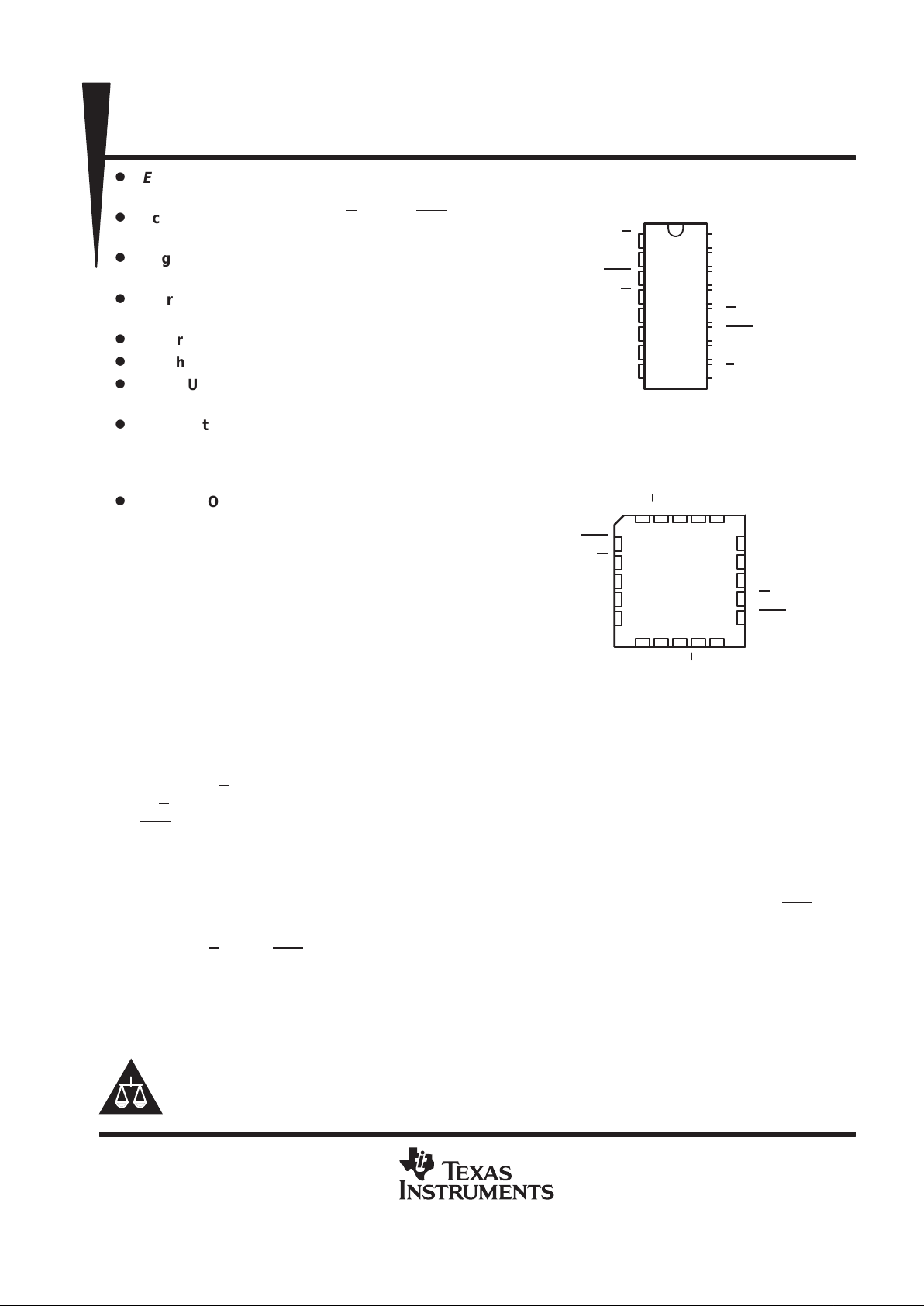
SN54LV123A...J OR W PACKAGE
SN74LV123A. . . D, DB, DGV, NS, OR PW PACKAGE
(TOP VIEW)
SN54LV123A. . . FK PACKAGE
(TOP VIEW)
1
2
3
4
5
6
7
8
16
15
14
13
12
11
10
9
1A
1B
1CLR
1Q
2Q
2C
ext
2R
ext/Cext
GND
V
CC
1R
ext/Cext
1C
ext
1Q
2Q
2CLR
2B
2A
3212019
910111213
4
5
6
7
8
18
17
16
15
14
1C
ext
1Q
NC
2Q
2CLR
1CLR
1Q
NC
2Q
2C
ext
1B1ANC
2A
2B
V
1R
2R
GND
NC
CC
NC – No internal connection
ext
/C
ext
ext
/C
ext
UNLESS OTHERWISE NOTED this document contains PRODUCTION
DATA information current as of publication date. Products conform to
specifications per the terms of Texas Instruments standard warranty.
Production processing does not necessarily include testing of all
parameters.
EPIC is a trademark of Texas Instruments Incorporated.
SN54LV123A, SN74LV123A
DUAL RETRIGGERABLE MONOSTABLE MULTIVIBRATORS
WITH SCHMITT-TRIGGER INPUTS
SCLS393A – APRIL 1998 – REVISED DECEMBER 1999
2
POST OFFICE BOX 655303 • DALLAS, TEXAS 75265
description (continued)
Once triggered, the basic pulse duration can be extended by retriggering the gated low-level-active (A) or
high-level-active (B) input. Pulse duration can be reduced by taking CLR low. The input/output timing diagram
illustrates pulse control by retriggering the inputs and early clearing.
The variance in output pulse duration from device to device typically is less than ±0.5% for given external timing
components. An example of this distribution for the ’LV123A is shown in Figure 11. Variations in output pulse
width versus supply voltage and temperature are shown in Figure 7.
During power up, Q outputs will be in the high state, and Q outputs will be in the low state. The outputs will be
glitch free without applying a reset pulse.
Pin assignments for these devices are identical to those of the ’AHC123A and ’AHCT123A devices for
interchangeability when allowed.
The SN54LV123A is characterized for operation over the full military temperature range of –55°C to 125°C.
The SN74LV123A is characterized for operation from –40°C to 85°C.
For additional application information on multivibrators, see the application report
Designing With The
SN74AHC123A and SN74AHCT123A
, literature number SCLA014.
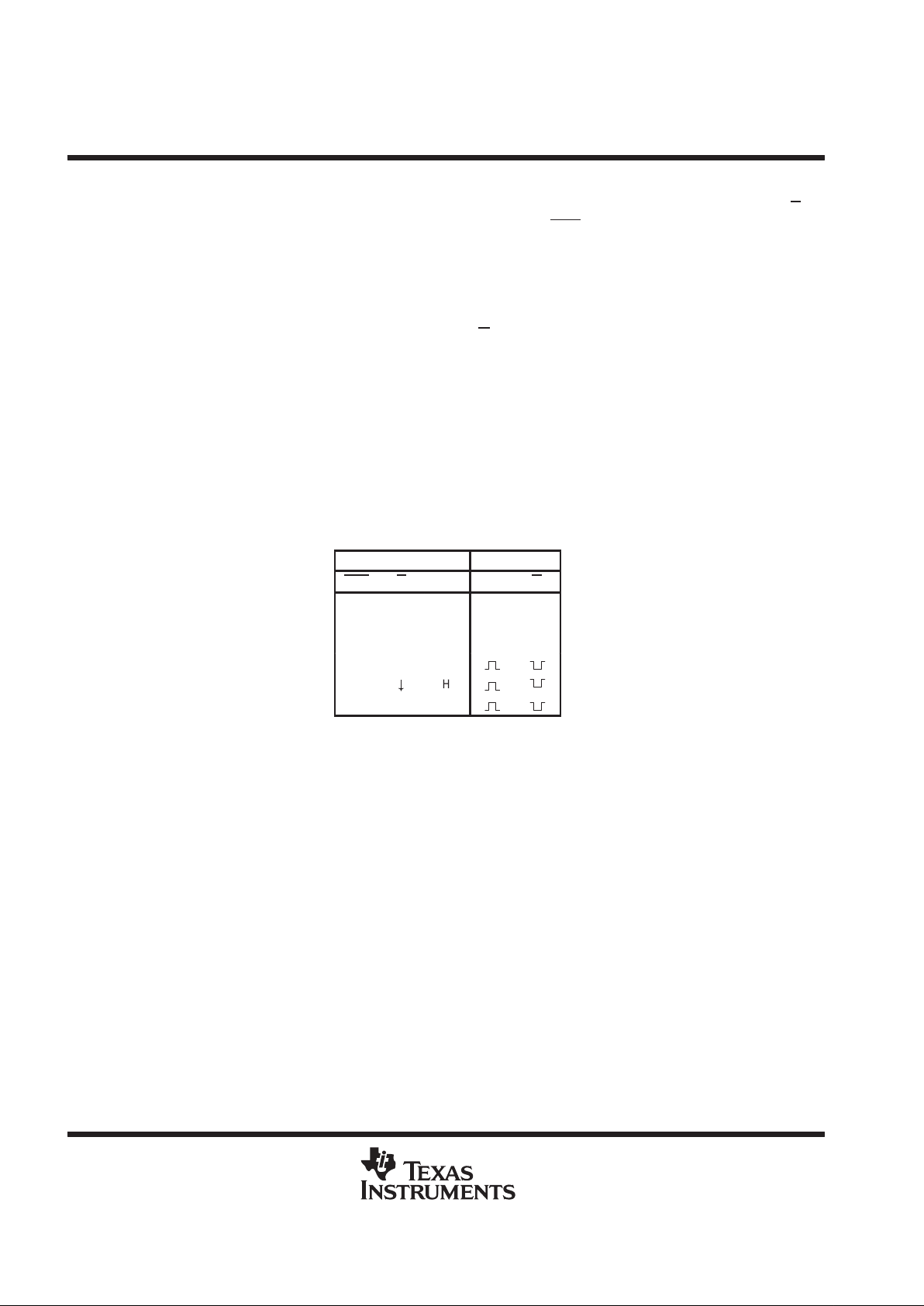
FUNCTION TABLE
(each multivibrator)
INPUTS OUTPUTS
CLR
A B Q Q
L X X L H
X HXL†H
†
X XLL†H
†
H L ↑
H
#
H
↑ L H
†
These outputs are based on the
assumption that the indicated steady-state
conditions at the A and B inputs have been
set up long enough to complete any pulse
started before the setup.
SN54LV123A, SN74LV123A
DUAL RETRIGGERABLE MONOSTABLE MULTIVIBRATORS
WITH SCHMITT-TRIGGER INPUTS
SCLS393A – APRIL 1998 – REVISED DECEMBER 1999
3
POST OFFICE BOX 655303 • DALLAS, TEXAS 75265
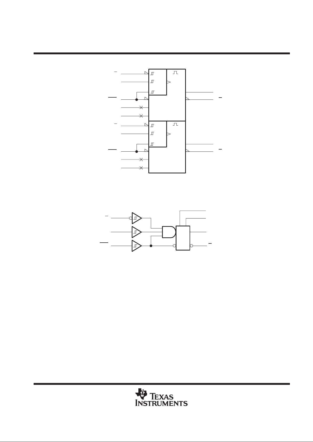
logic symbol
†
R
3
CX
14
4
1Q
13
RX/CX
15
1
1A
2
1B
&
R
11
CX
6
12
2Q
5
RX/CX
7
9
2A
10
2B
&
1CLR
2CLR
1C
ext
2C
ext
1R
ext/Cext
2R
ext/Cext
1Q
2Q
†
This symbol is in accordance with ANSI/IEEE Std 91-1984 and IEC Publication 617-12.
Pin numbers shown are for the D, DB, J, N, PW, and W packages.
logic diagram, each multivibrator (positive logic)
CLR
C
ext
R
ext/Cext
R
B
A
Q
Q
SN54LV123A, SN74LV123A
DUAL RETRIGGERABLE MONOSTABLE MULTIVIBRATORS
WITH SCHMITT-TRIGGER INPUTS
SCLS393A – APRIL 1998 – REVISED DECEMBER 1999
4
POST OFFICE BOX 655303 • DALLAS, TEXAS 75265
input/output timing diagram
A
B
CLR
Q
Q
t
w
t
w
tw + t
rr
t
rr
R
ext/Cext
absolute maximum ratings over operating free-air temperature (unless otherwise noted)
†
Supply voltage range, VCC –0.5 V to 7 V. . . . . . . . . . . . . . . . . . . . . . . . . . . . . . . . . . . . . . . . . . . . . . . . . . . . . . . . . .
Input voltage range, VI (see Note 1) –0.5 V to 7 V. . . . . . . . . . . . . . . . . . . . . . . . . . . . . . . . . . . . . . . . . . . . . . . . . .
Output voltage range in high or low state, V
O
(see Notes 1 and 2) –0.5 V to VCC + 0.5 V. . . . . . . . . . . . . . . . .
Output voltage range in power-off state, VO (see Note 1) –0.5 V to 7 V. . . . . . . . . . . . . . . . . . . . . . . . . . . . . . . .
Input clamp current, IIK (VI < 0) –20 mA. . . . . . . . . . . . . . . . . . . . . . . . . . . . . . . . . . . . . . . . . . . . . . . . . . . . . . . . . . .
Output clamp current, IOK (VO < 0 or VO > VCC) ±50 mA. . . . . . . . . . . . . . . . . . . . . . . . . . . . . . . . . . . . . . . . . . . .
Continuous output current, IO (VO = 0 to VCC) ±25 mA. . . . . . . . . . . . . . . . . . . . . . . . . . . . . . . . . . . . . . . . . . . . . .
Continuous current through V
CC
or GND ±50 mA. . . . . . . . . . . . . . . . . . . . . . . . . . . . . . . . . . . . . . . . . . . . . . . . . . .
Package thermal impedance, θJA (see Note 3): D package 113°C/W. . . . . . . . . . . . . . . . . . . . . . . . . . . . . . . . . .
DB package 131°C/W. . . . . . . . . . . . . . . . . . . . . . . . . . . . . . . .
DGV package 180°C/W. . . . . . . . . . . . . . . . . . . . . . . . . . . . . . .
NS package 111°C/W. . . . . . . . . . . . . . . . . . . . . . . . . . . . . . . .
PW package 149°C/W. . . . . . . . . . . . . . . . . . . . . . . . . . . . . . . .
Storage temperature range, T
stg
–65°C to 150°C. . . . . . . . . . . . . . . . . . . . . . . . . . . . . . . . . . . . . . . . . . . . . . . . . . .
†
Stresses beyond those listed under “absolute maximum ratings” may cause permanent damage to the device. These are stress ratings only, and
functional operation of the device at these or any other conditions beyond those indicated under “recommended operating conditions” is not
implied. Exposure to absolute-maximum-rated conditions for extended periods may affect device reliability.
NOTES: 1. The input and output voltage ratings may be exceeded if the input and output current ratings are observed.
2. This value is limited to 7 V maximum.
3. The package thermal impedance is calculated in accordance with JESD 51.
SN54LV123A, SN74LV123A
DUAL RETRIGGERABLE MONOSTABLE MULTIVIBRATORS
WITH SCHMITT-TRIGGER INPUTS
SCLS393A – APRIL 1998 – REVISED DECEMBER 1999
5
POST OFFICE BOX 655303 • DALLAS, TEXAS 75265
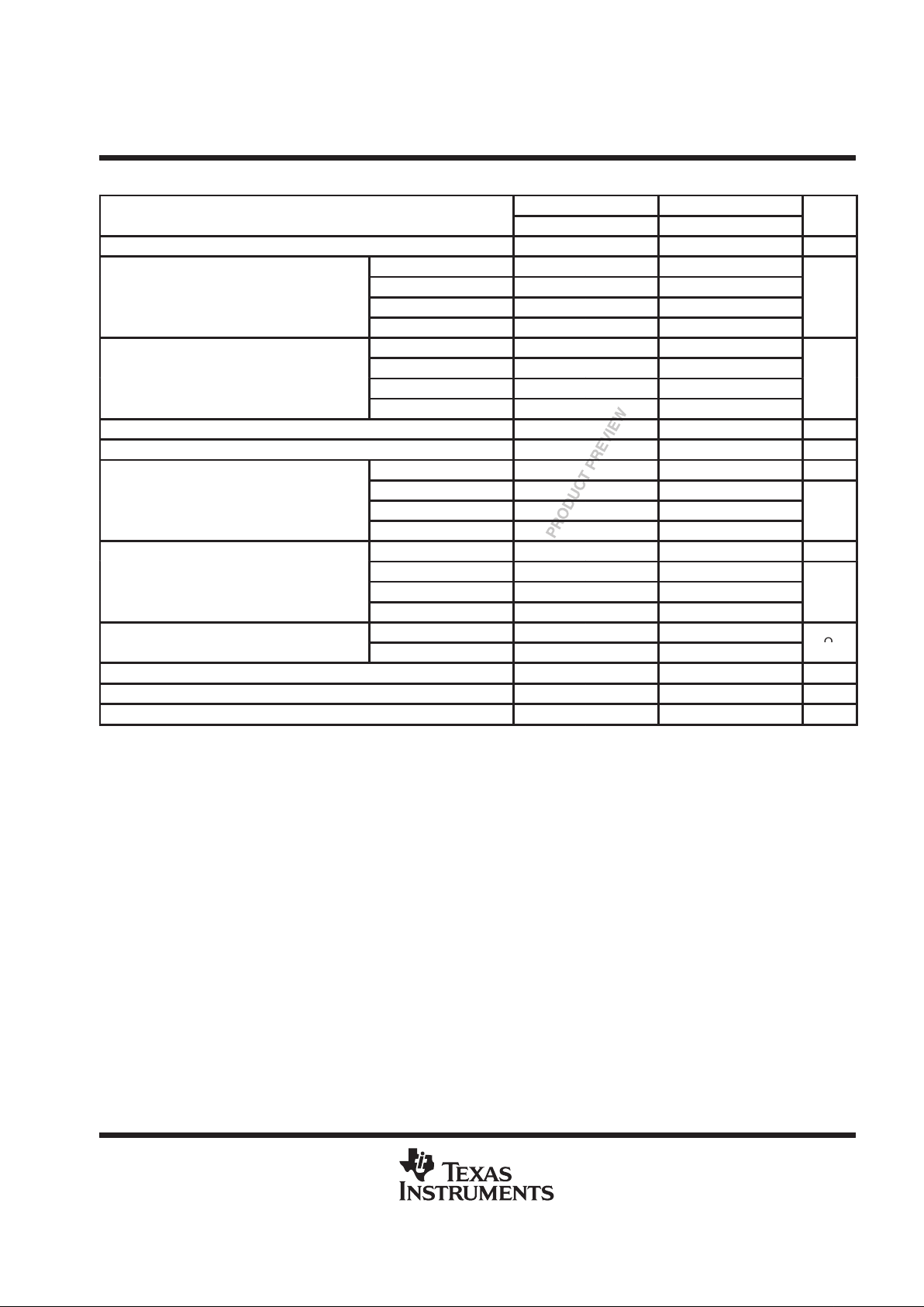
recommended operating conditions (see Note 4)
SN54LV123A SN74LV123A
MIN MAX MIN MAX
UNIT
V
CC
Supply voltage 2 5.5 2 5.5 V
VCC = 2 V 1.5 1.5
p
VCC = 2.3 V to 2.7 V VCC × 0.7 VCC × 0.7
VIHHigh-level input voltage
VCC = 3 V to 3.6 V VCC × 0.7 VCC × 0.7
V
VCC = 4.5 V to 5.5 V VCC × 0.7 VCC × 0.7
VCC = 2 V 0.5 0.5
p
VCC = 2.3 V to 2.7 V VCC × 0.3 VCC × 0.3
VILLow-level input voltage
VCC = 3 V to 3.6 V VCC × 0.3 VCC × 0.3
V
VCC = 4.5 V to 5.5 V VCC × 0.3 VCC × 0.3
V
I
Input voltage 0 5.5 0 5.5 V
V
O
Output voltage 0 V
CC
0 V
CC
V
VCC = 2 V –50 –50 µA
p
VCC = 2.3 V to 2.7 V –2 –2
IOHHigh-level output current
VCC = 3 V to 3.6 V –6 –6
mA
VCC = 4.5 V to 5.5 V –12 –12
VCC = 2 V 50 50 µA
p
VCC = 2.3 V to 2.7 V 2 2
IOLLow-level output current
VCC = 3 V to 3.6 V 6 6
mA
VCC = 4.5 V to 5.5 V 12 12
VCC = 2 V 5k 5k
R
ext
External timing resistance
VCC ≥ 3 V 1k 1k
Ω
C
ext
External timing capacitance No restriction No restriction pF
∆t/∆V
CC
Power-up ramp rate 1 1 ms/V
T
A
Operating free-air temperature –55 125 –40 85 °C
NOTE 4: All unused inputs of the device must be held at VCC or GND to ensure proper device operation. Refer to the TI application report,
Implications of Slow or Floating CMOS Inputs
, literature number SCBA004.
PRODUCT PREVIEW information concerns products in the formative or
design phase of development. Characteristic data and other
specifications are design goals. Texas Instruments reserves the right to
change or discontinue these products without notice.

SN54LV123A, SN74LV123A
DUAL RETRIGGERABLE MONOSTABLE MULTIVIBRATORS
WITH SCHMITT-TRIGGER INPUTS
SCLS393A – APRIL 1998 – REVISED DECEMBER 1999
6
POST OFFICE BOX 655303 • DALLAS, TEXAS 75265
electrical characteristics over recommended operating free-air temperature range (unless
otherwise noted)
SN54LV123A SN74LV123A
PARAMETER
TEST CONDITIONS
V
CC
MIN TYP MAX MIN TYP MAX
UNIT
IOH = –50 µA 2 V to 5.5 V VCC–0.1 VCC–0.1
IOH = –2 mA 2.3 V 2 2
V
OH
IOH = –6 mA 3 V 2.48 2.48
V
IOH = –12 mA 4.5 V 3.8 3.8
IOL = 50 µA 2 V to 5.5 V 0.1 0.1
IOL = 2 mA 2.3 V 0.4 0.4
V
OL
IOL = 6 mA 3 V 0.44 0.44
V
IOL = 12 mA 4.5 V 0.55 0.55
R
ext/Cext
†
VI = VCC or GND 2 V to 5.5 V ±2.5 ±2.5
I
I
0 V ±1 ±1
µA
A, B
, and
CLR
V
I
=
V
CC
or GND
5.5 V ±1 ±1
I
CC
Quiescent VI = VCC or GND, IO = 0 5.5 V 20 20 µA
2.3 V 220 220
Active state V
= V
or GND,
3 V 280 280
I
CC
(per circuit)
ICC
,
R
ext/Cext
= 0.5 V
CC
4.5 V 650 650
µ
A
5.5 V 975 975
I
off
VI or VO = 0 to 5.5 V 0 V 5 µA
3.3 V 1.9 1.9
p
CiV
I
=
V
CC
or GND
5 V 1.9 1.9
pF
†
This test is performed with the terminal in the off-state condition.
timing requirements over recommended operating free-air temperature range, VCC = 2.5 V ± 0.2 V
(unless otherwise noted) (see Figure 1)
TA = 25°C SN54LV123A SN74LV123A
TEST CONDITIONS
MIN TYP MAX MIN MAX MIN MAX
UNIT
Pulse
CLR 6 6.5 6.5
t
w
duration
A
or B trigger 6 6.5 6.5
ns
C
ext
= 100 pF
‡
94
‡ ‡
ns
t
rr
Pul
se retrigger time
R
ext
=
1 kΩ
C
ext
= 0.01 mF
‡
2
‡ ‡
m
s
‡
See retriggering data in the
application information
section.
timing requirements over recommended operating free-air temperature range, VCC = 3.3 V ± 0.3 V
(unless otherwise noted) (see Figure 1)
TA = 25°C SN54LV123A SN74LV123A
TEST CONDITIONS
MIN TYP MAX MIN MAX MIN MAX
UNIT
Pulse
CLR 5 5 5
t
w
duration
A
or B trigger 5 5 5
ns
C
ext
= 100 pF
‡
76
‡ ‡
ns
t
rr
Pul
se retrigger time
R
ext
=
1 kΩ
C
ext
= 0.01 mF
‡
1.8
‡ ‡
m
s
‡
See retriggering data in the
application information
section.
PRODUCT PREVIEW information concerns products in the formative or
design phase of development. Characteristic data and other
specifications are design goals. Texas Instruments reserves the right to
change or discontinue these products without notice.

SN54LV123A, SN74LV123A
DUAL RETRIGGERABLE MONOSTABLE MULTIVIBRATORS
WITH SCHMITT-TRIGGER INPUTS
SCLS393A – APRIL 1998 – REVISED DECEMBER 1999
7
POST OFFICE BOX 655303 • DALLAS, TEXAS 75265
timing requirements over recommended operating free-air temperature range, VCC = 5 V ± 0.5 V
(unless otherwise noted) (see Figure 1)
TA = 25°C SN54LV123A SN74LV123A
TEST CONDITIONS
MIN TYP MAX MIN MAX MIN MAX
UNIT
Pulse
CLR 5 5 5
t
w
duration
A
or B trigger 5 5 5
ns
C
ext
= 100 pF
†
59
† †
ns
t
rr
Pul
se retrigger time
R
ext
=
1 kΩ
C
ext
= 0.01 mF
†
1.5
† †
m
s
†
See retriggering data in the
application information
section.
switching characteristics over recommended operating free-air temperature range,
V
CC
= 2.5 V ± 0.2 V (unless otherwise noted) (see Figure 1)
FROM TO TEST
TA = 25°C SN54LV123A SN74LV123A
PARAMETER
(INPUT) (OUTPUT) CONDITIONS
MIN TYP MAX MIN MAX MIN MAX
UNIT
A or B Q or Q
14.5* 31.4* 1* 37* 11 37
t
pd
CLR
Q or Q
CL = 15 pF
13* 25* 1* 29.5* 1 29.5
ns
CLR trigger Q or Q
15.1* 33.4* 1* 39* 1 39
A or B Q or Q
16.6 36 1 42 1 42
t
pd
CLR
Q or Q
CL = 50 pF
14.7 32.8 1 34.5 1 34.5
ns
CLR trigger Q or Q
17.4 38 1 44 1 44
CL = 50 pF,
C
ext
= 28 pF,
R
ext
= 2 kΩ
197 260 320 320 ns
t
w
‡
Q or Q
CL = 50 pF,
C
ext
= 0.01 µF,
R
ext
= 10 kΩ
90 100 110 90 110 90 110
m
s
CL = 50 pF,
C
ext
= 0.1 µF,
R
ext
= 10 kΩ
0.9 1 1.1 0.9 1.1 0.9 1.1 ms
∆t
w
§
CL = 50 pF ±1 %
* On products compliant to MIL-PRF-38535, this parameter is not production tested.
‡
tw = Duration of pulse at Q and Q
outputs
§
∆tw = Output pulse duration variation (Q and Q
) between circuits in same package
PRODUCT PREVIEW information concerns products in the formative or
design phase of development. Characteristic data and other
specifications are design goals. Texas Instruments reserves the right to
change or discontinue these products without notice.

SN54LV123A, SN74LV123A
DUAL RETRIGGERABLE MONOSTABLE MULTIVIBRATORS
WITH SCHMITT-TRIGGER INPUTS
SCLS393A – APRIL 1998 – REVISED DECEMBER 1999
8
POST OFFICE BOX 655303 • DALLAS, TEXAS 75265
switching characteristics over recommended operating free-air temperature range,
V
CC
= 3.3 V ± 0.3 V (unless otherwise noted) (see Figure 1)
FROM TO TEST
TA = 25°C SN54LV123A SN74LV123A
PARAMETER
(INPUT) (OUTPUT) CONDITIONS
MIN TYP MAX MIN MAX MIN MAX
UNIT
A or B Q or Q
10.2* 20.6* 1* 24* 1 24
t
pd
CLR
Q or Q
CL = 15 pF
9.3* 15.8* 1* 18.5* 1 18.5
ns
CLR trigger Q or Q
10.6* 22.4* 1* 26* 1 26
A or B Q or Q
11.8 24.1 1 27.5 1 27.5
t
pd
CLR
Q or Q
CL = 50 pF
10.5 19.3 1 22 1 22
ns
CLR trigger Q or Q
12.3 25.9 1 29.5 1 29.5
CL = 50 pF,
C
ext
= 28 pF,
R
ext
= 2 kΩ
182 240 300 300 ns
t
w
†
Q or Q
CL = 50 pF,
C
ext
= 0.01 µF,
R
ext
= 10 kΩ
90 100 110 90 110 90 110
m
s
CL = 50 pF,
C
ext
= 0.1 µF,
R
ext
= 10 kΩ
0.9 1 1.1 0.9 1.1 0.9 1.1 ms
∆t
w
‡
CL = 50 pF ±1 %
* On products compliant to MIL-PRF-38535, this parameter is not production tested.
†
tw = Duration of pulse at Q and Q
outputs
‡
∆tw = Output pulse duration variation (Q and Q
) between circuits in same package
switching characteristics over recommended operating free-air temperature range,
V
CC
= 5 V ± 0.5 V (unless otherwise noted) (see Figure 1)
FROM TO TEST
TA = 25°C SN54LV123A SN74LV123A
PARAMETER
(INPUT) (OUTPUT) CONDITIONS
MIN TYP MAX MIN MAX MIN MAX
UNIT
A or B Q or Q
7.1* 12* 1* 14* 1 14
t
pd
CLR
Q or Q
CL = 15 pF
6.5* 9.4* 1* 11* 1 11
ns
CLR trigger Q or Q
7.4* 12.9* 1* 15* 1 15
A or B Q or Q
8.3 14 1 16 1 16
t
pd
CLR
Q or Q
CL = 50 pF
7.4 11.4 1 13 1 13
ns
CLR trigger Q or Q
8.7 14.9 1 17 1 17
CL = 50 pF,
C
ext
= 28 pF,
R
ext
= 2 kΩ
167 200 240 240 ns
t
w
†
Q or Q
CL = 50 pF,
C
ext
= 0.01 µF,
R
ext
= 10 kΩ
90 100 110 90 110 90 110
m
s
CL = 50 pF,
C
ext
= 0.1 µF,
R
ext
= 10 kΩ
0.9 1 1.1 0.9 1.1 0.9 1.1 ms
∆t
w
‡
±1 %
* On products compliant to MIL-PRF-38535, this parameter is not production tested.
†
tw = Duration of pulse at Q and Q
outputs
‡
∆tw = Output pulse duration variation (Q and Q
) between circuits in same package
PRODUCT PREVIEW information concerns products in the formative or
design phase of development. Characteristic data and other
specifications are design goals. Texas Instruments reserves the right to
change or discontinue these products without notice.

SN54LV123A, SN74LV123A
DUAL RETRIGGERABLE MONOSTABLE MULTIVIBRATORS
WITH SCHMITT-TRIGGER INPUTS
SCLS393A – APRIL 1998 – REVISED DECEMBER 1999
9
POST OFFICE BOX 655303 • DALLAS, TEXAS 75265
operating characteristics, T
A
= 25°C
PARAMETER
TEST CONDITIONS V
CC
TYP UNIT
p
p
p
3.3 V 44
p
CpdPower dissipation capacitance
C
L
= 50 pF,f = 10 MHz
5 V 49
pF
PARAMETER MEASUREMENT INFORMATION
NOTES: A. CL includes probe and jig capacitance.
B. All input pulses are supplied by generators having the following characteristics: PRR ≤ 1 MHz, ZO = 50 Ω, tr +3 ns, tf + 3 ns.
C. The outputs are measured one at a time with one input transition per measurement.
50% V
CC
t
PLH
t
PHL
V
OH
V
OL
V
CC
50% V
CC
50% V
CC
V
CC
Input A
(see Note B)
50% V
CC
0 V
0 V
In-Phase
Output
Out-of-Phase
Output
VOLTAGE WAVEFORMS
DELA Y TIMES
Input B
(see Note B)
V
OL
V
OH
LOAD CIRCUIT
Test
Point
C
L
(see Note A)
From Output
Under Test
50% V
CC
t
PLH
t
PHL
t
PHL
t
PLH
V
OH
V
OH
V
OL
V
OL
V
CC
0 V
50% V
CC
Input CLR
(see Note B)
Out-of-Phase
Output
In-Phase
Output
VOLTAGE WAVEFORMS
DELA Y TIMES
50% V
CC
50% V
CC
50% V
CC
50% V
CC
V
CC
0 V
t
w
VOLTAGE WAVEFORMS
PULSE DURATION
Inputs or
Outputs
50% V
CC
50% V
CC
Figure 1. Load Circuit and Voltage Waveforms

SN54LV123A, SN74LV123A
DUAL RETRIGGERABLE MONOSTABLE MULTIVIBRATORS
WITH SCHMITT-TRIGGER INPUTS
SCLS393A – APRIL 1998 – REVISED DECEMBER 1999
10
POST OFFICE BOX 655303 • DALLAS, TEXAS 75265
APPLICATION INFORMATION
caution in use
To prevent malfunctions due to noise, connect a high-frequency capacitor between VCC and GND, and keep
the wiring between the external components and C
ext
and R
ext/Cext
terminals as short as possible.
power-down considerations
Large values of C
ext
may cause problems when powering down the ’L V123A because of the amount of energy
stored in the capacitor. When a system containing this device is powered down, the capacitor may discharge
from VCC through the protection diodes at pin 2 or pin 14. Current through the input protection diodes must be
limited to 30 mA; therefore, the turn-off time of the V
CC
power supply must not be faster than
t = V
CC
× C
ext
/30 mA. For example, if VCC = 5 V and C
ext
= 15 pF , the VCC supply must turn off no faster than
t = (5 V) × (15 pF)/30mA = 2.5 ms. Usually, this is not a problem because power supplies are heavily filtered
and cannot discharge at this rate. When a more rapid decrease of VCC to zero occurs, the ’L V123A may sustain
damage. To avoid this possibility, use external clamping diodes.
output pulse duration
The output pulse duration, tw, is determined primarily by the values of the external capacitance (CT) and timing
resistance (R
T
). The timing components are connected as shown in Figure 2.
V
CC
R
T
C
T
To R
ext/Cext
Terminal
To C
ext
Terminal
Figure 2. Timing-Component Connections
The pulse duration is given by:
t
w
+K
RT
C
T
if CT is ≥ 1000 pF, K = 1.0
or
if CT is < 1000 pF, K can be determined from Figure 9
where:
tw= pulse duration in ns
RT= external timing resistance in kΩ
CT= external capacitance in pF
K = multiplier factor
Equation 1 and Figures 5 or 6 can be used to determine values for pulse duration, external resistance, and
external capacitance.
(1)

SN54LV123A, SN74LV123A
DUAL RETRIGGERABLE MONOSTABLE MULTIVIBRATORS
WITH SCHMITT-TRIGGER INPUTS
SCLS393A – APRIL 1998 – REVISED DECEMBER 1999
11
POST OFFICE BOX 655303 • DALLAS, TEXAS 75265
APPLICATION INFORMATION
retriggering data
The minimum input retriggering time (t
MIR
) is the minimum time required after the initial signal before retriggering the
input. After t
MIR
, the device retriggers the output. Experimentally, it also can be shown that, to retrigger the output
pulse, the two adjacent input signals should be t
MIR
apart, where t
MIR
= 0.30 × tw. The retrigger pulse duration is
calculated as shown in Figure 3.
t
MIR
t
RT
t
PLH
t
w
Input
Output
tRT = tw + t
PLH
= (K × RT × CT) + t
PLH
Where:
t
MIR
= Minimum Input Retriggering Time
t
PLH
= Propagation Delay
tRT= Retrigger Time
tw= Output Pulse Duration Before Retriggering
Figure 3. Retrigger Pulse Duration
The minimum value from the end of the input pulse to the beginning of the retriggered output should be approximately
15 ns to ensure a retriggered output. This is illustrated in Figure 4.
Input
Output
t
MRT
= Minimum Time Between the End of the Second Input Pulse and the Beginning of the Retriggered Output
t
MRT
= 15 ns
t
MRT
Figure 4. Input/Output Requirements

SN54LV123A, SN74LV123A
DUAL RETRIGGERABLE MONOSTABLE MULTIVIBRATORS
WITH SCHMITT-TRIGGER INPUTS
SCLS393A – APRIL 1998 – REVISED DECEMBER 1999
12
POST OFFICE BOX 655303 • DALLAS, TEXAS 75265
APPLICATION INFORMATION
†
Figure 5
OUTPUT PULSE DURATION
vs
EXTERNAL TIMING CAPACITANCE
1.00E+07
t
w
– Output Pulse Duration – ns
1.00E+06
1.00E+05
1.00E+04
1.00E+03
1.00E+02
CT – External Timing Capacitance – pF
10
1
10
2
10
3
10
4
10
5
VCC = 3 V
TA = 25°C
RT = 1 MΩ
RT = 100 kΩ
RT = 10 kΩ
RT = 1 kΩ
Figure 6
OUTPUT PULSE DURATION
vs
EXTERNAL TIMING CAPACITANCE
1.00E+07
t
w
– Output Pulse Duration – ns
1.00E+06
1.00E+05
1.00E+04
1.00E+03
1.00E+02
CT – External Timing Capacitance – pF
10
1
10
2
10
3
10
4
10
5
RT = 1 MΩ
RT = 100 kΩ
RT = 10 kΩ
RT = 1 kΩ
VCC = 4.5 V
TA = 25°C
tw = 866 ns at:
VCC = 5 V
RT = 10 kΩ
CT = 50 pF
TA = 25°C
–60 –40 –20 0 20 40 60 80 100 120 140 160
VCC = 2.5 V
VCC = 3 V
VCC = 3.5 V
VCC = 4 V
VCC = 5 V
VCC = 6 V
VCC = 7 V
180
–6%
–4%
–2%
0%
2%
4%
6%
8%
10%
12%
14%
Temperature – °C
Variation in Output Pulse Duration
VARIATION IN OUTPUT PULSE DURATION
vs
TEMPERATURE
Figure 7
†
Operation of the device at these or any other conditions beyond those indicated under “recommended operating conditions” is not implied.

SN54LV123A, SN74LV123A
DUAL RETRIGGERABLE MONOSTABLE MULTIVIBRATORS
WITH SCHMITT-TRIGGER INPUTS
SCLS393A – APRIL 1998 – REVISED DECEMBER 1999
13
POST OFFICE BOX 655303 • DALLAS, TEXAS 75265
APPLICATION INFORMATION
†
Figure 8
MINIMUM TRIGGER TIME
vs
V
CC
CHARACTERISTICS
RT = 1 kΩ
TA = 25°C
10.00
0
1.00
0.10
0.01
123456
CT = 0.01 µF
CT = 1000 pF
CT = 100 pF
VCC –
Supply Voltage –
V
Minimum Retrigger Time–
µ
s
rr
– t
Figure 9
1.20
1.15
1.10
1.05
1.00
0.95
0.90
1.5 2 2.5 3 3.5 4 4.5 5 5.5 6
RT = 10 kΩ
TA = 25°C
tw = K × CT × R
T
VCC – Supply Voltage – V
OUTPUT PULSE DURATION CONSTANT
vs
SUPPLY VOLTAGE
Output Pulse Duration Constant – K
CT = 1000 pF
CT = 0.01 µF
CT = 0.1 µF
Figure 10
1.00 1.50 2.00 2.50 3.00 3.50 4.00 4.50
0.00001
0.0001
0.001
TA = 25°C
VCC = 5 V
For Capacitor Values of
0.001 µF or Greater, K = 1.0
(K is Independent of R)
Multiplier Factor – K
EXTERNAL CAPACITANCE
vs
MULTIPLIER FACTOR
C
T
– External Capacitor Value –
µ
F
Figure 11
tw – Output Pulse Duration
Relative Frequency of Occurrence
DISTRIBUTION OF UNITS
vs
OUTPUT PULSE DURATION
Mean = 856 ns
Median = 856 ns
Std. Dev. = 3.5 ns
VCC = 5 V
TA = 25°C
CT = 50 pF
RT = 10 kΩ
–3 Std. Dev. +3 Std. Dev.
Median
99% of Data Units
†
Operation of the device at these or any other conditions beyond those indicated under “recommended operating conditions” is not implied.

IMPORTANT NOTICE
T exas Instruments and its subsidiaries (TI) reserve the right to make changes to their products or to discontinue
any product or service without notice, and advise customers to obtain the latest version of relevant information
to verify, before placing orders, that information being relied on is current and complete. All products are sold
subject to the terms and conditions of sale supplied at the time of order acknowledgement, including those
pertaining to warranty, patent infringement, and limitation of liability.
TI warrants performance of its semiconductor products to the specifications applicable at the time of sale in
accordance with TI’s standard warranty. Testing and other quality control techniques are utilized to the extent
TI deems necessary to support this warranty. Specific testing of all parameters of each device is not necessarily
performed, except those mandated by government requirements.
CERT AIN APPLICATIONS USING SEMICONDUCTOR PRODUCTS MAY INVOLVE POTENTIAL RISKS OF
DEATH, PERSONAL INJURY, OR SEVERE PROPERTY OR ENVIRONMENTAL DAMAGE (“CRITICAL
APPLICATIONS”). TI SEMICONDUCTOR PRODUCTS ARE NOT DESIGNED, AUTHORIZED, OR
WARRANTED TO BE SUITABLE FOR USE IN LIFE-SUPPORT DEVICES OR SYSTEMS OR OTHER
CRITICAL APPLICATIONS. INCLUSION OF TI PRODUCTS IN SUCH APPLICA TIONS IS UNDERSTOOD T O
BE FULLY AT THE CUSTOMER’S RISK.
In order to minimize risks associated with the customer’s applications, adequate design and operating
safeguards must be provided by the customer to minimize inherent or procedural hazards.
TI assumes no liability for applications assistance or customer product design. TI does not warrant or represent
that any license, either express or implied, is granted under any patent right, copyright, mask work right, or other
intellectual property right of TI covering or relating to any combination, machine, or process in which such
semiconductor products or services might be or are used. TI’s publication of information regarding any third
party’s products or services does not constitute TI’s approval, warranty or endorsement thereof.
Copyright 1999, Texas Instruments Incorporated
 Loading...