

Texas Instruments SN74LV123ADR, SN74LV123ANS, SN74LV123ANSR, SN74LV123APWR, SN74LV123AD Datasheet
...
SN54LV123A, SN74LV123A
DUAL RETRIGGERABLE MONOSTABLE MULTIVIBRATORS
WITH SCHMITT-TRIGGER INPUTS
SCLS393A – APRIL 1998 – REVISED DECEMBER 1999
1
POST OFFICE BOX 655303 • DALLAS, TEXAS 75265
D
EPIC
(Enhanced-Performance Implanted
CMOS) Process
D
Schmitt-Trigger Circuitry on A, B, and CLR
Inputs for Slow Input Transition Rates
D
Edge Triggered From Active-High or
Active-Low Gated Logic Inputs
D
Retriggerable for Very Long Output Pulses,
up to 100% Duty Cycle
D
Overriding Clear Terminates Output Pulse
D
Glitch-Free Power-Up Reset on Outputs
D
Latch-Up Performance Exceeds 100 mA Per
JESD 78, Class II
D
ESD Protection Exceeds JESD 22
– 2000-V Human-Body Model (A114-A)
– 200-V Machine Model (A115-A)
– 1000-V Charged-Device Model (C101)
D
Package Options Include Plastic
Small-Outline (D, NS), Shrink Small-Outline
(DB), Thin Very Small-Outline (DGV), and
Thin Shrink Small-Outline (PW) Packages,
Ceramic Flat (W) Packages, Chip Carriers
(FK), and DIPs (J)
description
The ’LV123A devices are dual retriggerable
monostable multivibrators designed for 2-V to
5.5-V VCC operation.
These edge-triggered multivibrators feature
output pulse-duration control by three methods. In
the first method, the A input is low and the B input
goes high. In the second method, the B input is
high and the A
input goes low. In the third method,
the A input is low, the B input is high, and the clear
(CLR) input goes high.
The output pulse duration is programmable by selecting external resistance and capacitance values. The
external timing capacitor must be connected between C
ext
and R
ext/Cext
(positive) and an external resistor
connected between R
ext/Cext
and VCC. To obtain variable pulse durations, connect an external variable
resistance between R
ext/Cext
and VCC. The output pulse duration can also be reduced by taking CLR low.
Pulse triggering occurs at a particular voltage level and is not directly related to the transition time of the input
pulse. The A, B, and CLR inputs have Schmitt triggers with sufficient hysteresis to handle slow input transition
rates with jitter-free triggering at the outputs.
Copyright 1999, Texas Instruments Incorporated
Please be aware that an important notice concerning availability, standard warranty, and use in critical applications of
Texas Instruments semiconductor products and disclaimers thereto appears at the end of this data sheet.
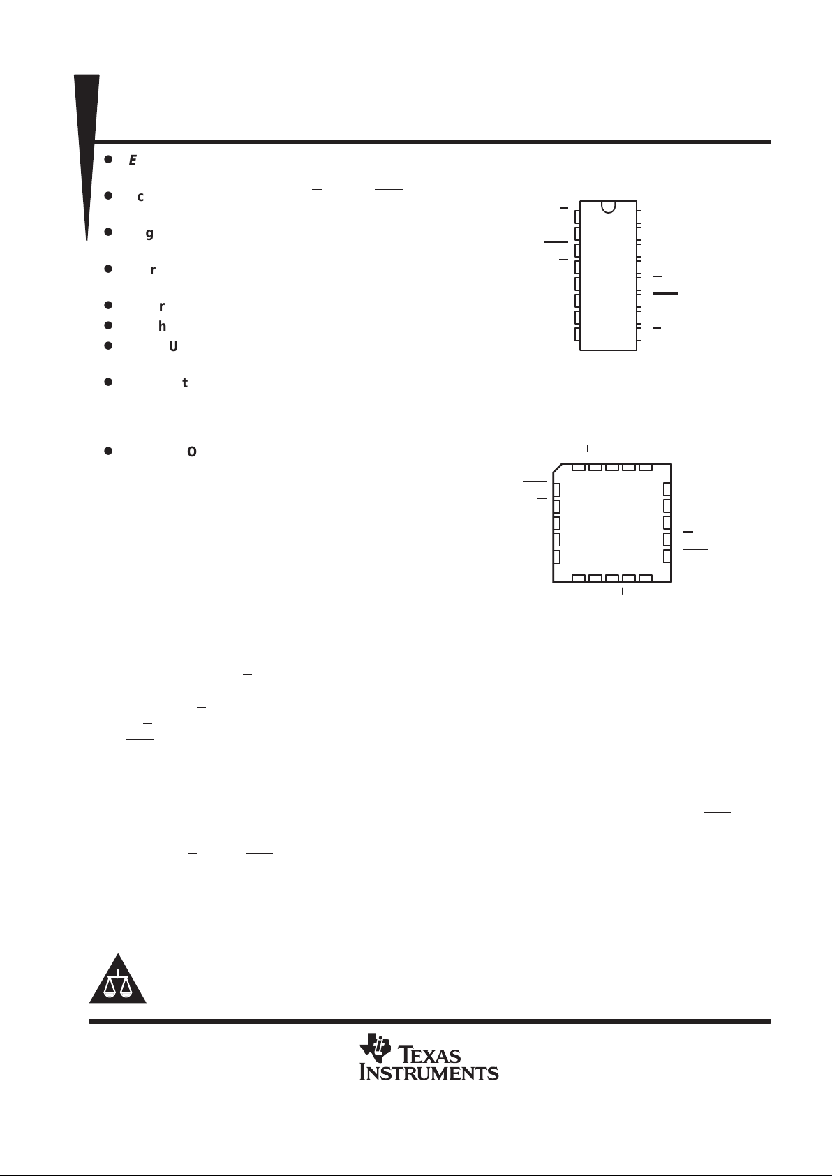
SN54LV123A...J OR W PACKAGE
SN74LV123A. . . D, DB, DGV, NS, OR PW PACKAGE
(TOP VIEW)
SN54LV123A. . . FK PACKAGE
(TOP VIEW)
1
2
3
4
5
6
7
8
16
15
14
13
12
11
10
9
1A
1B
1CLR
1Q
2Q
2C
ext
2R
ext/Cext
GND
V
CC
1R
ext/Cext
1C
ext
1Q
2Q
2CLR
2B
2A
3212019
910111213
4
5
6
7
8
18
17
16
15
14
1C
ext
1Q
NC
2Q
2CLR
1CLR
1Q
NC
2Q
2C
ext
1B1ANC
2A
2B
V
1R
2R
GND
NC
CC
NC – No internal connection
ext
/C
ext
ext
/C
ext
UNLESS OTHERWISE NOTED this document contains PRODUCTION
DATA information current as of publication date. Products conform to
specifications per the terms of Texas Instruments standard warranty.
Production processing does not necessarily include testing of all
parameters.
EPIC is a trademark of Texas Instruments Incorporated.
SN54LV123A, SN74LV123A
DUAL RETRIGGERABLE MONOSTABLE MULTIVIBRATORS
WITH SCHMITT-TRIGGER INPUTS
SCLS393A – APRIL 1998 – REVISED DECEMBER 1999
2
POST OFFICE BOX 655303 • DALLAS, TEXAS 75265
description (continued)
Once triggered, the basic pulse duration can be extended by retriggering the gated low-level-active (A) or
high-level-active (B) input. Pulse duration can be reduced by taking CLR low. The input/output timing diagram
illustrates pulse control by retriggering the inputs and early clearing.
The variance in output pulse duration from device to device typically is less than ±0.5% for given external timing
components. An example of this distribution for the ’LV123A is shown in Figure 11. Variations in output pulse
width versus supply voltage and temperature are shown in Figure 7.
During power up, Q outputs will be in the high state, and Q outputs will be in the low state. The outputs will be
glitch free without applying a reset pulse.
Pin assignments for these devices are identical to those of the ’AHC123A and ’AHCT123A devices for
interchangeability when allowed.
The SN54LV123A is characterized for operation over the full military temperature range of –55°C to 125°C.
The SN74LV123A is characterized for operation from –40°C to 85°C.
For additional application information on multivibrators, see the application report
Designing With The
SN74AHC123A and SN74AHCT123A
, literature number SCLA014.
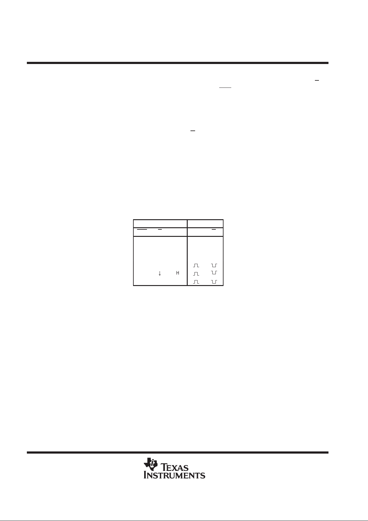
FUNCTION TABLE
(each multivibrator)
INPUTS OUTPUTS
CLR
A B Q Q
L X X L H
X HXL†H
†
X XLL†H
†
H L ↑
H
#
H
↑ L H
†
These outputs are based on the
assumption that the indicated steady-state
conditions at the A and B inputs have been
set up long enough to complete any pulse
started before the setup.
SN54LV123A, SN74LV123A
DUAL RETRIGGERABLE MONOSTABLE MULTIVIBRATORS
WITH SCHMITT-TRIGGER INPUTS
SCLS393A – APRIL 1998 – REVISED DECEMBER 1999
3
POST OFFICE BOX 655303 • DALLAS, TEXAS 75265
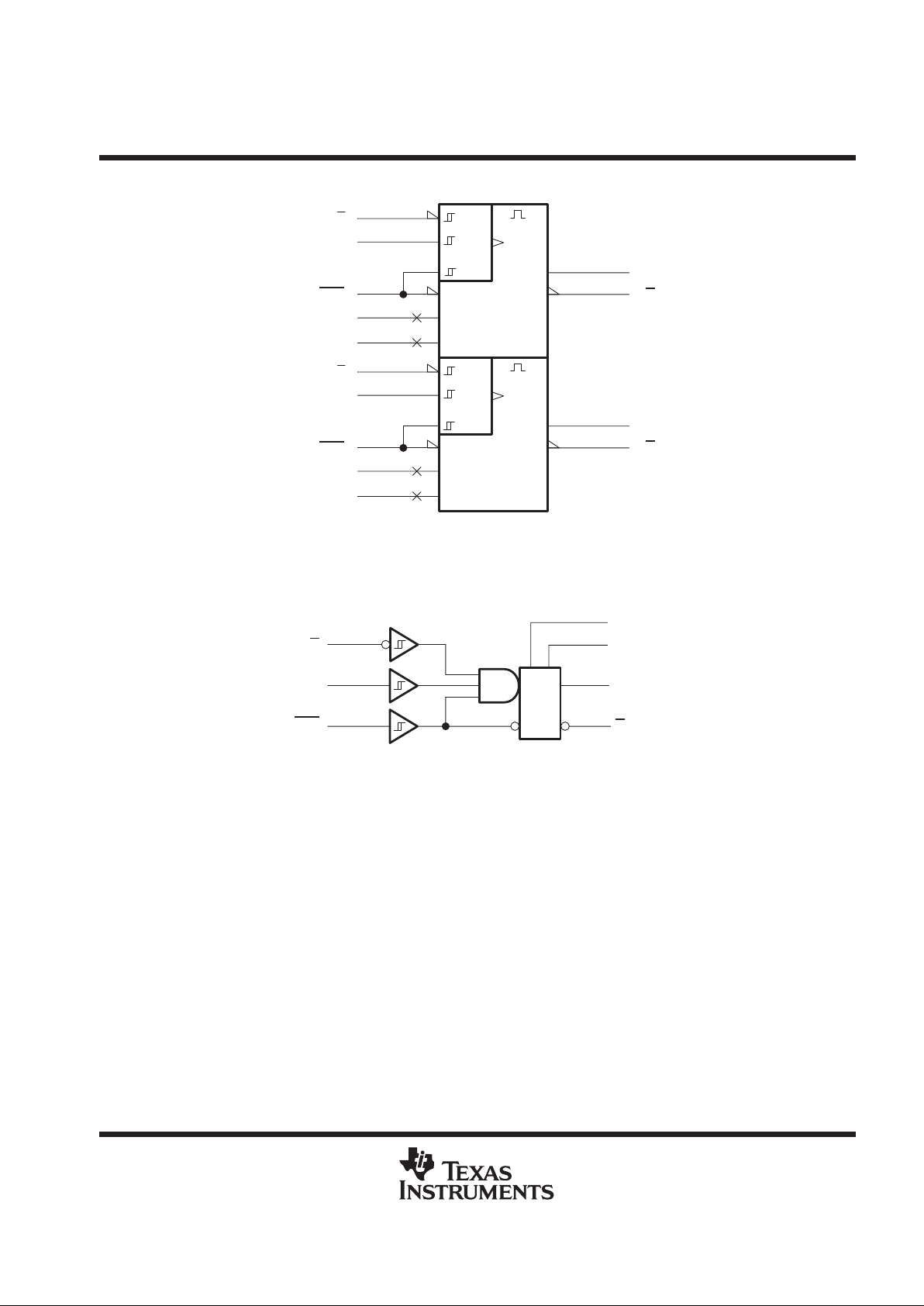
logic symbol
†
R
3
CX
14
4
1Q
13
RX/CX
15
1
1A
2
1B
&
R
11
CX
6
12
2Q
5
RX/CX
7
9
2A
10
2B
&
1CLR
2CLR
1C
ext
2C
ext
1R
ext/Cext
2R
ext/Cext
1Q
2Q
†
This symbol is in accordance with ANSI/IEEE Std 91-1984 and IEC Publication 617-12.
Pin numbers shown are for the D, DB, J, N, PW, and W packages.
logic diagram, each multivibrator (positive logic)
CLR
C
ext
R
ext/Cext
R
B
A
Q
Q
SN54LV123A, SN74LV123A
DUAL RETRIGGERABLE MONOSTABLE MULTIVIBRATORS
WITH SCHMITT-TRIGGER INPUTS
SCLS393A – APRIL 1998 – REVISED DECEMBER 1999
4
POST OFFICE BOX 655303 • DALLAS, TEXAS 75265
input/output timing diagram
A
B
CLR
Q
Q
t
w
t
w
tw + t
rr
t
rr
R
ext/Cext
absolute maximum ratings over operating free-air temperature (unless otherwise noted)
†
Supply voltage range, VCC –0.5 V to 7 V. . . . . . . . . . . . . . . . . . . . . . . . . . . . . . . . . . . . . . . . . . . . . . . . . . . . . . . . . .
Input voltage range, VI (see Note 1) –0.5 V to 7 V. . . . . . . . . . . . . . . . . . . . . . . . . . . . . . . . . . . . . . . . . . . . . . . . . .
Output voltage range in high or low state, V
O
(see Notes 1 and 2) –0.5 V to VCC + 0.5 V. . . . . . . . . . . . . . . . .
Output voltage range in power-off state, VO (see Note 1) –0.5 V to 7 V. . . . . . . . . . . . . . . . . . . . . . . . . . . . . . . .
Input clamp current, IIK (VI < 0) –20 mA. . . . . . . . . . . . . . . . . . . . . . . . . . . . . . . . . . . . . . . . . . . . . . . . . . . . . . . . . . .
Output clamp current, IOK (VO < 0 or VO > VCC) ±50 mA. . . . . . . . . . . . . . . . . . . . . . . . . . . . . . . . . . . . . . . . . . . .
Continuous output current, IO (VO = 0 to VCC) ±25 mA. . . . . . . . . . . . . . . . . . . . . . . . . . . . . . . . . . . . . . . . . . . . . .
Continuous current through V
CC
or GND ±50 mA. . . . . . . . . . . . . . . . . . . . . . . . . . . . . . . . . . . . . . . . . . . . . . . . . . .
Package thermal impedance, θJA (see Note 3): D package 113°C/W. . . . . . . . . . . . . . . . . . . . . . . . . . . . . . . . . .
DB package 131°C/W. . . . . . . . . . . . . . . . . . . . . . . . . . . . . . . .
DGV package 180°C/W. . . . . . . . . . . . . . . . . . . . . . . . . . . . . . .
NS package 111°C/W. . . . . . . . . . . . . . . . . . . . . . . . . . . . . . . .
PW package 149°C/W. . . . . . . . . . . . . . . . . . . . . . . . . . . . . . . .
Storage temperature range, T
stg
–65°C to 150°C. . . . . . . . . . . . . . . . . . . . . . . . . . . . . . . . . . . . . . . . . . . . . . . . . . .
†
Stresses beyond those listed under “absolute maximum ratings” may cause permanent damage to the device. These are stress ratings only, and
functional operation of the device at these or any other conditions beyond those indicated under “recommended operating conditions” is not
implied. Exposure to absolute-maximum-rated conditions for extended periods may affect device reliability.
NOTES: 1. The input and output voltage ratings may be exceeded if the input and output current ratings are observed.
2. This value is limited to 7 V maximum.
3. The package thermal impedance is calculated in accordance with JESD 51.
SN54LV123A, SN74LV123A
DUAL RETRIGGERABLE MONOSTABLE MULTIVIBRATORS
WITH SCHMITT-TRIGGER INPUTS
SCLS393A – APRIL 1998 – REVISED DECEMBER 1999
5
POST OFFICE BOX 655303 • DALLAS, TEXAS 75265
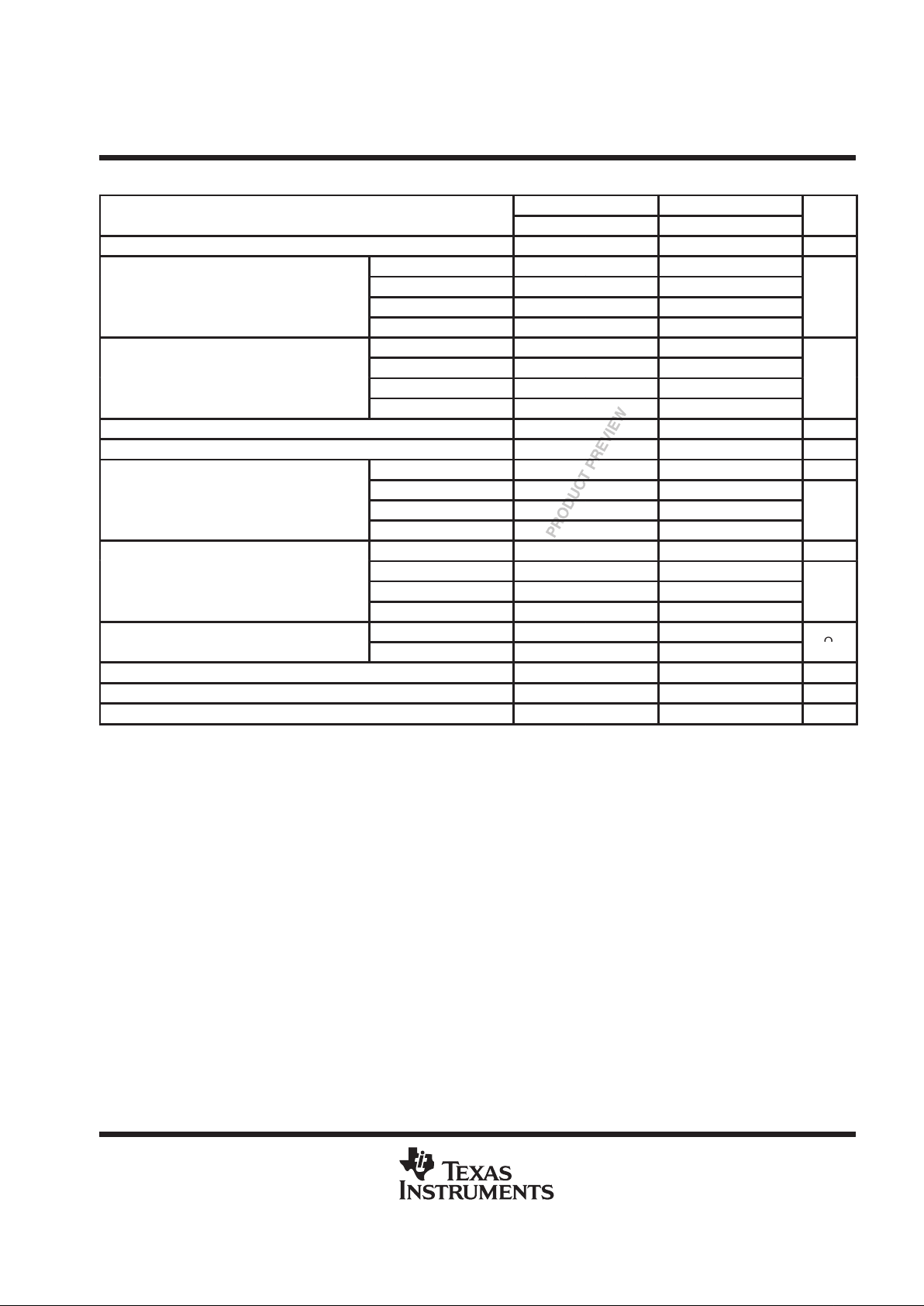
recommended operating conditions (see Note 4)
SN54LV123A SN74LV123A
MIN MAX MIN MAX
UNIT
V
CC
Supply voltage 2 5.5 2 5.5 V
VCC = 2 V 1.5 1.5
p
VCC = 2.3 V to 2.7 V VCC × 0.7 VCC × 0.7
VIHHigh-level input voltage
VCC = 3 V to 3.6 V VCC × 0.7 VCC × 0.7
V
VCC = 4.5 V to 5.5 V VCC × 0.7 VCC × 0.7
VCC = 2 V 0.5 0.5
p
VCC = 2.3 V to 2.7 V VCC × 0.3 VCC × 0.3
VILLow-level input voltage
VCC = 3 V to 3.6 V VCC × 0.3 VCC × 0.3
V
VCC = 4.5 V to 5.5 V VCC × 0.3 VCC × 0.3
V
I
Input voltage 0 5.5 0 5.5 V
V
O
Output voltage 0 V
CC
0 V
CC
V
VCC = 2 V –50 –50 µA
p
VCC = 2.3 V to 2.7 V –2 –2
IOHHigh-level output current
VCC = 3 V to 3.6 V –6 –6
mA
VCC = 4.5 V to 5.5 V –12 –12
VCC = 2 V 50 50 µA
p
VCC = 2.3 V to 2.7 V 2 2
IOLLow-level output current
VCC = 3 V to 3.6 V 6 6
mA
VCC = 4.5 V to 5.5 V 12 12
VCC = 2 V 5k 5k
R
ext
External timing resistance
VCC ≥ 3 V 1k 1k
Ω
C
ext
External timing capacitance No restriction No restriction pF
∆t/∆V
CC
Power-up ramp rate 1 1 ms/V
T
A
Operating free-air temperature –55 125 –40 85 °C
NOTE 4: All unused inputs of the device must be held at VCC or GND to ensure proper device operation. Refer to the TI application report,
Implications of Slow or Floating CMOS Inputs
, literature number SCBA004.
PRODUCT PREVIEW information concerns products in the formative or
design phase of development. Characteristic data and other
specifications are design goals. Texas Instruments reserves the right to
change or discontinue these products without notice.
 Loading...