

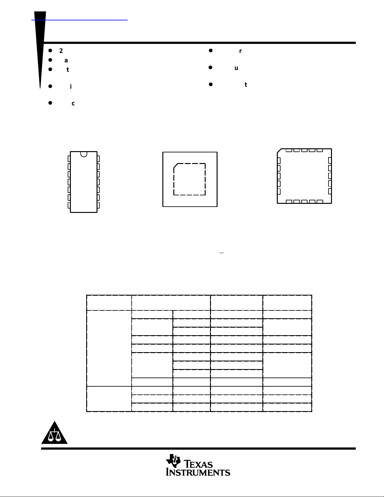
SOIC
D
LV04A
查询SN74LV04ADGVR供应商
D
2-V to 5.5-V VCC Operation
D
Max t
D
Latch-Up Performance Exceeds 250 mA Per
of 6.5 ns at 5 V
pd
JESD 17
D
Typical V
<0.8 V at V
D
Typical V
>2.3 V at V
(Output Ground Bounce)
OLP
= 3.3 V, TA = 25°C
CC
(Output VOH Undershoot)
OHV
= 3.3 V, TA = 25°C
CC
SN54LV04A, SN74LV04A
HEX INVERTERS
SCLS388H – SEPTEMBER 1997 – REVISED JUL Y 2003
D
Support Mixed-Mode Voltage Operation on
All Ports
D
I
Supports Partial-Power-Down Mode
off
Operation
D
ESD Protection Exceeds JESD 22
– 2000-V Human-Body Model (A114-A)
– 200-V Machine Model (A115-A)
– 1000-V Charged-Device Model (C101)
SN54LV04A...J OR W PACKAGE
SN74LV04A. . . D, DB, DGV, NS,
OR PW PACKAGE
(TOP VIEW)
1A
1Y
2A
2Y
3A
3Y
GND
1
2
3
4
5
6
7
14
13
12
11
10
V
CC
6A
6Y
5A
5Y
9
4A
8
4Y
SN74LV04A. . . RGY PACKAGE
1Y
2A
2Y
3A
3Y
(TOP VIEW)
1A
114
2
3
4
5
6
78
CC
V
13
12
11
10
6A
6Y
5A
5Y
9
4A
4Y
GND
SN54LV04A. . . FK PACKAGE
2A
NC
2Y
NC
3A
NC – No internal connection
(TOP VIEW)
1Y1ANC
3212019
4
5
6
7
8
910111213
3Y
NC
GND
CC
V
4Y
description/ordering information
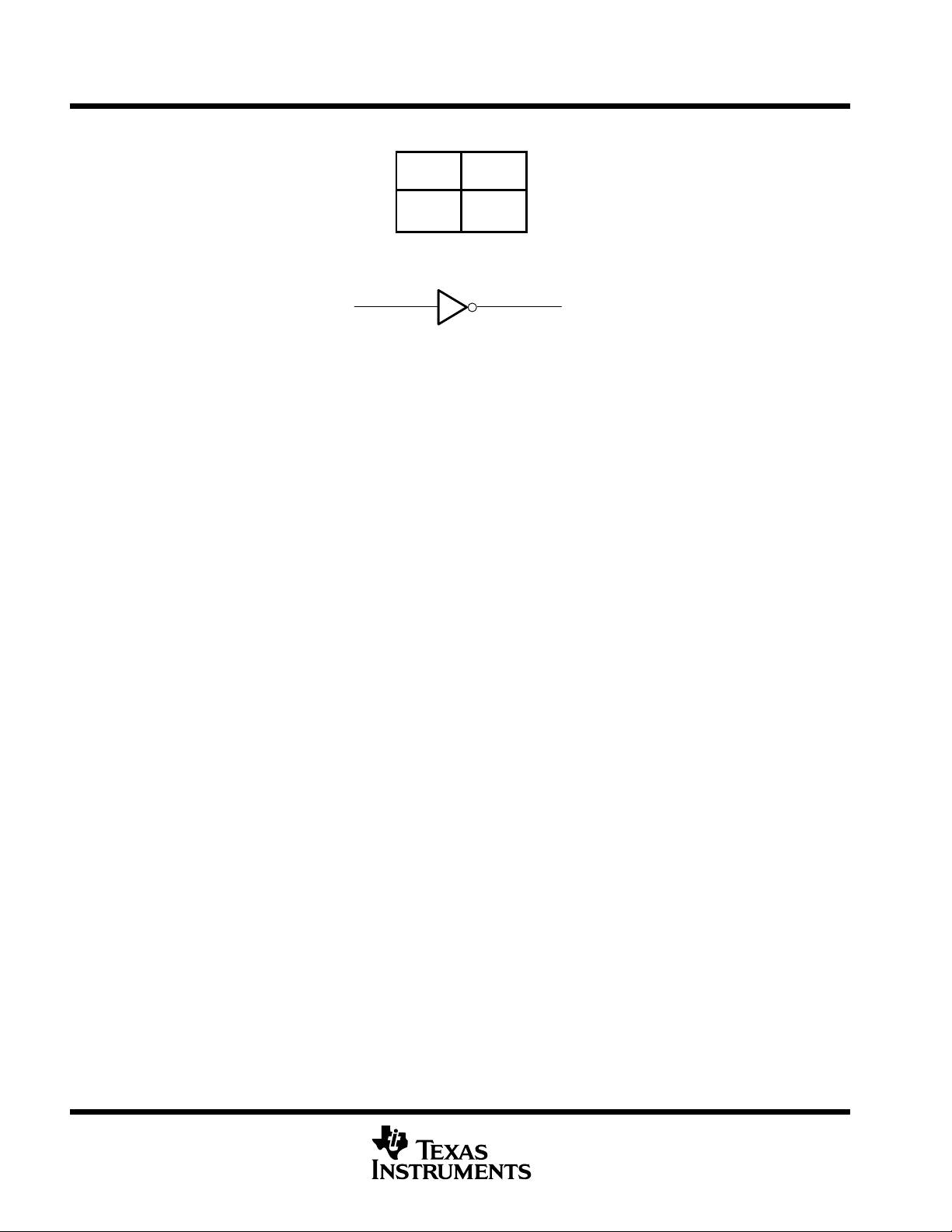
These hex inverters are designed for 2-V to 5.5-V VCC operation. The ’L V04A devices contain six independent
inverters. These devices perform the Boolean function Y = A
These devices are fully specified for partial-power-down applications using I
outputs, preventing damaging current backflow through the devices when they are powered down.
ORDERING INFORMA TION
T
A
QFN – RGY Reel of 1000 SN74LV04ARGYR LV04A
SOP – NS Reel of 2000 SN74LV04ANSR 74LV04A
–40°C to 85°C
–55°C to 125°C
†
Package drawings, standard packing quantities, thermal data, symbolization, and PCB design
guidelines are available at www.ti.com/sc/package.
Please be aware that an important notice concerning availability, standard warranty, and use in critical applications of
Texas Instruments semiconductor products and disclaimers thereto appears at the end of this data sheet.
SSOP – DB Reel of 2000 SN74LV04ADBR LV04A
TSSOP – PW
TVSOP – DGV Reel of 2000 SN74LV04ADGVR LV04A
CDIP – J Tube of 25 SNJ54LV04AJ SNJ54LV04AJ
CFP – W T ube of 150 SNJ54LV04AW SNJ54LV04AW
LCCC – FK Tube of 55 SNJ54LV04AFK SNJ54LV04AFK
PACKAGE
–
†
Tube of 50 SN74LV04AD
Reel of 2500 SN74LV04ADR
Tube of 90 SN74LV04APW
Reel of 2000 SN74LV04APWR
Reel of 250 SN74LV04APWT
.
ORDERABLE
PART NUMBER
. The I
off
TOP-SIDE
MARKING
LV04A
circuitry disables the
off
6A
18
17
16
15
14
4A
6Y
NC
5A
NC
5Y
UNLESS OTHERWISE NOTED this document contains PRODUCTION
DATA information current as of publication date. Products conform to
specifications per the terms of Texas Instruments standard warranty.
Production processing does not necessarily include testing of all
parameters.
POST OFFICE BOX 655303 • DALLAS, TEXAS 75265
Copyright 2003, Texas Instruments Incorporated
1
SN54LV04A, SN74LV04A
HEX INVERTERS
SCLS388H – SEPTEMBER 1997 – REVISED JULY 2003
FUNCTION TABLE
INPUT
logic diagram, each inverter (positive logic)
(each inverter)
OUTPUT
A
H L
L H
Y
YA
absolute maximum ratings over operating free-air temperature range (unless otherwise noted)
Supply voltage range, V
Input voltage range, V
Voltage range applied to any output in the high-impedance
or power-off state, V
Output voltage range, V
Input clamp current, I
Output clamp current, I
Continuous output current, I
Continuous current through V
Package thermal impedance, θ
Storage temperature range, T
†
Stresses beyond those listed under “absolute maximum ratings” may cause permanent damage to the device. These are stress ratings only, and
functional operation of the device at these or any other conditions beyond those indicated under “recommended operating conditions” is not
implied. Exposure to absolute-maximum-rated conditions for extended periods may affect device reliability.
NOTES: 1. The input and output voltage ratings may be exceeded if the input and output current ratings are observed.
2. This value is limited to 5.5 V maximum.
3. The package thermal impedance is calculated in accordance with JESD 51-7.
4. The package thermal impedance is calculated in accordance with JESD 51-5.
–0.5 V to 7 V. . . . . . . . . . . . . . . . . . . . . . . . . . . . . . . . . . . . . . . . . . . . . . . . . . . . . . . . . .
CC
(see Note 1) –0.5 V to 7 V. . . . . . . . . . . . . . . . . . . . . . . . . . . . . . . . . . . . . . . . . . . . . . . . . .
I
(see Note 1) –0.5 V to 7 V. . . . . . . . . . . . . . . . . . . . . . . . . . . . . . . . . . . . . . . . . . . . . . . .
O
(see Notes 1 and 2) –0.5 V to VCC + 0.5 V. . . . . . . . . . . . . . . . . . . . . . . . . . . . . . . . . .
O
(VI < 0) –20 mA. . . . . . . . . . . . . . . . . . . . . . . . . . . . . . . . . . . . . . . . . . . . . . . . . . . . . . . . . . .
IK
(VO < 0 or VO > VCC) ±50 mA. . . . . . . . . . . . . . . . . . . . . . . . . . . . . . . . . . . . . . . . . . . .
OK
(VO = 0 to VCC) ±25 mA. . . . . . . . . . . . . . . . . . . . . . . . . . . . . . . . . . . . . . . . . . . . . .
O
or GND ±50 mA. . . . . . . . . . . . . . . . . . . . . . . . . . . . . . . . . . . . . . . . . . . . . . . . . . .
CC
(see Note 3): D package 86°C/W. . . . . . . . . . . . . . . . . . . . . . . . . . . . . . . . . . .
JA
(see Note 3): DB package 96°C/W. . . . . . . . . . . . . . . . . . . . . . . . . . . . . . . . .
(see Note 3): DGV package 127°C/W. . . . . . . . . . . . . . . . . . . . . . . . . . . . . . .
(see Note 3): NS package 76°C/W. . . . . . . . . . . . . . . . . . . . . . . . . . . . . . . . .
(see Note 3): PW package 113°C/W. . . . . . . . . . . . . . . . . . . . . . . . . . . . . . . .
(see Note 4): RGY package 47°C/W. . . . . . . . . . . . . . . . . . . . . . . . . . . . . . . .
–65°C to 150°C. . . . . . . . . . . . . . . . . . . . . . . . . . . . . . . . . . . . . . . . . . . . . . . . . . .
stg
†
2
POST OFFICE BOX 655303 • DALLAS, TEXAS 75265
UNIT
VIHHigh-level input voltage
V
VILLow-level input voltage
V
IOHHigh-level output current
IOLLow-level output current
PARAMETER
TEST CONDITIONS
V
UNIT
V
V
V
V
C
V
V
or GND
pF
SN54LV04A, SN74LV04A
HEX INVERTERS
SCLS388H – SEPTEMBER 1997 – REVISED JULY 2003
recommended operating conditions (see Note 5)
SN54LV04A SN74LV04A
MIN MAX MIN MAX
V
Supply voltage 2 5.5 2 5.5 V
CC
VCC = 2 V 1.5 1.5
p
p
V
Input voltage 0 5.5 0 5.5 V
I
V
Output voltage 0 V
O
p
p
∆t/∆v Input transition rise or fall rate
T
Operating free-air temperature –55 125 –40 85 °C
A
NOTE 5: All unused inputs of the device must be held at VCC or GND to ensure proper device operation. Refer to the TI application report,
Implications of Slow or Floating CMOS Inputs, literature number SCBA004.
VCC = 2.3 V to 2.7 V VCC× 0.7 VCC× 0.7
VCC = 3 V to 3.6 V VCC× 0.7 VCC× 0.7
VCC = 4.5 V to 5.5 V VCC× 0.7 VCC× 0.7
VCC = 2 V 0.5 0.5
VCC = 2.3 V to 2.7 V VCC× 0.3 VCC× 0.3
VCC = 3 V to 3.6 V VCC× 0.3 VCC× 0.3
VCC = 4.5 V to 5.5 V VCC× 0.3 VCC× 0.3
CC
VCC = 2 V –50 –50 µA
VCC = 2.3 V to 2.7 V –2 –2
VCC = 3 V to 3.6 V –6 –6
VCC = 4.5 V to 5.5 V –12 –12
VCC = 2 V 50 50 µA
VCC = 2.3 V to 2.7 V 2 2
VCC = 3 V to 3.6 V 6 6
VCC = 4.5 V to 5.5 V 12 12
VCC = 2.3 V to 2.7 V 200 200
VCC = 3 V to 3.6 V
VCC = 4.5 V to 5.5 V 20 20
100 100
0 V
CC
mA
mA
ns/V
V
electrical characteristics over recommended operating free-air temperature range (unless
otherwise noted)
SN54LV04A SN74LV04A
MIN TYP MAX MIN TYP MAX
p
IOH = –50 µA 2 V to 5.5 V VCC–0.1 VCC–0.1
OH
OL
I
I
I
CC
I
off
i
PRODUCT PREVIEW information concerns products in the formative or
design phase of development. Characteristic data and other
specifications are design goals. Texas Instruments reserves the right to
change or discontinue these products without notice.
IOH = –2 mA 2.3 V 2 2
IOH = –6 mA 3 V 2.48 2.48
IOH = –12 mA 4.5 V 3.8 3.8
IOL = 50 µA 2 V to 5.5 V 0.1 0.1
IOL = 2 mA 2.3 V 0.4 0.4
IOL = 6 mA 3 V 0.44 0.44
IOL = 12 mA 4.5 V 0.55 0.55
VI = 5.5 V or GND 0 to 5.5 V ±1 ±1 µA
VI = VCC or GND, IO = 0 5.5 V 20 20 µA
VI or VO = 0 to 5.5 V 0 5 5 µA
=
I
CC
CC
3.3 V 2.3 2.3
5 V 2.3 2.3
POST OFFICE BOX 655303 • DALLAS, TEXAS 75265
3
SN54LV04A, SN74LV04A
PARAMETER
UNIT
t
d
A
Y
ns
PARAMETER
UNIT
t
d
A
Y
ns
PARAMETER
UNIT
t
d
A
Y
ns
PARAMETER
UNIT
C
d
Power dissi ation ca acitance
C
L
MHz
F
HEX INVERTERS
SCLS388H – SEPTEMBER 1997 – REVISED JULY 2003
switching characteristics over recommended operating free-air temperature range,
VCC = 2.5 V ± 0.2 V (unless otherwise noted) (see Figure 1)
FROM TO LOAD
(INPUT) (OUTPUT) CAPACITANCE
p
* On products compliant to MIL-PRF-38535, this parameter is not production tested.
CL = 15 pF 7.1* 11.7* 1* 14* 1 14
CL = 50 pF 10 15.5 1 18 1 18
switching characteristics over recommended operating free-air temperature range,
VCC = 3.3 V ± 0.3 V (unless otherwise noted) (see Figure 1)
FROM TO LOAD
(INPUT) (OUTPUT) CAPACITANCE
p
* On products compliant to MIL-PRF-38535, this parameter is not production tested.
CL = 15 pF 5.1* 7.1* 1* 8.5* 1 8.5
CL = 50 pF 7.3 10.6 1 12 1 12
switching characteristics over recommended operating free-air temperature range,
= 5 V ± 0.5 V (unless otherwise noted) (see Figure 1)
V
CC
FROM TO LOAD
(INPUT) (OUTPUT) CAPACITANCE
p
* On products compliant to MIL-PRF-38535, this parameter is not production tested.
CL = 15 pF 3.6* 5.5* 1* 6.5* 1 6.5
CL = 50 pF 5.1 7.5 1 8.5 1 8.5
TA = 25°C SN54LV04A SN74LV04A
MIN TYP MAX MIN MAX MIN MAX
TA = 25°C SN54LV04A SN74LV04A
MIN TYP MAX MIN MAX MIN MAX
TA = 25°C SN54LV04A SN74LV04A
MIN TYP MAX MIN MAX MIN MAX
noise characteristics, VCC = 3.3 V, CL = 50 pF, TA = 25°C (see Note 6)
V
OL(P)
V
OL(V)
V
OH(V)
V
IH(D)
V
IL(D)
NOTE 6: Characteristics are for surface-mount packages only.
Quiet output, maximum dynamic V
Quiet output, minimum dynamic V
Quiet output, minimum dynamic V
High-level dynamic input voltage 2.31 V
Low-level dynamic input voltage 0.99 V
OL
OL
OH
operating characteristics, TA = 25°C
PARAMETER TEST CONDITIONS V
p
p
p
p
= 50 F,f = 10
SN74LV04A
MIN TYP MAX
0.3 0.8 V
–0.1 –0.8 V
3.1 V
TYP UNIT
CC
3.3 V 9.6
5 V 11.4
p
PRODUCT PREVIEW information concerns products in the formative or
design phase of development. Characteristic data and other
specifications are design goals. Texas Instruments reserves the right to
change or discontinue these products without notice.
4
POST OFFICE BOX 655303 • DALLAS, TEXAS 75265

From Output
Under Test
(see Note A)
SN54LV04A, SN74LV04A
HEX INVERTERS
SCLS388H – SEPTEMBER 1997 – REVISED JULY 2003
PARAMETER MEASUREMENT INFORMATION
V
Test
Point
C
L
From Output
Under Test
(see Note A)
C
L
RL = 1 kΩ
S1
CC
Open
GND
TEST S1
t
PLH/tPHL
t
PLZ/tPZL
t
PHZ/tPZH
Open Drain
Open
V
CC
GND
V
CC
LOAD CIRCUIT FOR
TOTEM-POLE OUTPUTS
t
w
Input
Input
In-Phase
Output
Out-of-Phase
Output
INVERTING AND NONINVERTING OUTPUTS
NOTES: A. CL includes probe and jig capacitance.
B. Waveform 1 is for an output with internal conditions such that the output is low except when disabled by the output control.
Waveform 2 is for an output with internal conditions such that the output is high except when disabled by the output control.
C. All input pulses are supplied by generators having the following characteristics: PRR ≤ 1 MHz, ZO = 50 Ω, tr ≤ 3 ns, tf ≤ 3 ns.
D. The outputs are measured one at a time with one input transition per measurement.
E. t
F. t
G. t
H. All parameters and waveforms are not applicable to all devices.
50% V
CC
VOLTAGE WAVEFORMS
PULSE DURATION
50% V
CC
t
PLH
50% V
t
PHL
50% V
VOLTAGE WAVEFORMS
PROPAGATION DELAY TIMES
PLZ
PZL
PHL
and t
and t
and t
are the same as t
PHZ
are the same as ten.
PZH
are the same as tpd.
PLH
50% V
50% V
CC
CC
dis
3-STATE AND OPEN-DRAIN OUTPUTS
CC
.
LOAD CIRCUIT FOR
V
CC
CC
0 V
V
CC
0 V
t
PHL
V
t
PLH
CC
V
V
CC
V
OH
OL
OH
OL
50% V
50% V
Timing Input
Data Input
Output
Control
Output
Waveform 1
S1 at V
(see Note B)
Waveform 2
(see Note B)
CC
Output
S1 at GND
50% V
CC
t
CC
CC
h
50% V
50% V
CC
CC
t
PLZ
VOL + 0.3 V
t
PHZ
VOH – 0.3 V
t
su
50% V
CC
VOLTAGE WAVEFORMS
SETUP AND HOLD TIMES
50% V
CC
t
PZL
50% V
t
PZH
50% V
VOLTAGE WAVEFORMS
ENABLE AND DISABLE TIMES
LOW- AND HIGH-LEVEL ENABLING
V
CC
0 V
V
CC
0 V
V
CC
0 V
≈V
V
OL
V
OH
≈0 V
CC
Figure 1. Load Circuit and Voltage Waveforms
POST OFFICE BOX 655303 • DALLAS, TEXAS 75265
5

MECHANICAL DATA
MPDS006C – FEBRUARY 1996 – REVISED AUGUST 2000
DGV (R-PDSO-G**) PLASTIC SMALL-OUTLINE
24 PINS SHOWN
0,40
24
112
A
0,23
0,13
13
0,07
4,50
4,30
M
6,60
6,20
0,16 NOM
Gage Plane
0,25
0°–8°
0,75
0,50
1,20 MAX
PINS **
DIM
A MAX
A MIN
NOTES: A. All linear dimensions are in millimeters.
B. This drawing is subject to change without notice.
C. Body dimensions do not include mold flash or protrusion, not to exceed 0,15 per side.
D. Falls within JEDEC: 24/48 Pins – MO-153
14/16/20/56 Pins – MO-194
0,15
0,05
14
3,70
3,50
Seating Plane
3,50
20
5,10
4,90
0,08
5,103,70
4,90
382416
7,90
7,70
48
9,80
9,60
56
11,40
11,20
4073251/E 08/00
POST OFFICE BOX 655303 • DALLAS, TEXAS 75265
1


MECHANICAL DATA
MSOI002B – JANUARY 1995 – REVISED SEPTEMBER 2001
D (R-PDSO-G**) PLASTIC SMALL-OUTLINE PACKAGE
8 PINS SHOWN
8 5
1 4
A
0.069 (1,75) MAX
0.020 (0,51)
0.014 (0,35)
0.157 (4,00)
0.150 (3,81)
0.010 (0,25)
0.004 (0,10)
0.244 (6,20)
0.228 (5,80)
0.010 (0,25)0.050 (1,27)
0.008 (0,20) NOM
Gage Plane
0.010 (0,25)
0°– 8°
0.044 (1,12)
0.016 (0,40)
Seating Plane
0.004 (0,10)
PINS **
DIM
A MAX
A MIN
NOTES: A. All linear dimensions are in inches (millimeters).
B. This drawing is subject to change without notice.
C. Body dimensions do not include mold flash or protrusion, not to exceed 0.006 (0,15).
D. Falls within JEDEC MS-012
8
0.197
(5,00)
0.189
(4,80)
14
0.344
(8,75)
0.337
(8,55)
16
0.394
(10,00)
0.386
(9,80)
4040047/E 09/01
POST OFFICE BOX 655303 • DALLAS, TEXAS 75265
1


MECHANICAL DATA
MSSO002E – JANUARY 1995 – REVISED DECEMBER 2001
DB (R-PDSO-G**) PLASTIC SMALL-OUTLINE
28 PINS SHOWN
0,65
28
1
2,00 MAX
0,38
0,22
15
14
A
0,05 MIN
0,15
5,60
5,00
M
8,20
7,40
Seating Plane
0,10
0,25
0,09
0°–ā8°
Gage Plane
0,25
0,95
0,55
PINS **
DIM
A MAX
A MIN
NOTES: A. All linear dimensions are in millimeters.
B. This drawing is subject to change without notice.
C. Body dimensions do not include mold flash or protrusion not to exceed 0,15.
D. Falls within JEDEC MO-150
14
6,50
6,50
5,905,90
2016
7,50
6,90
24
8,50
28
10,50
9,907,90
30
10,50
9,90
38
12,90
12,30
4040065 /E 12/01
POST OFFICE BOX 655303 • DALLAS, TEXAS 75265
1

MECHANICAL DATA
MTSS001C – JANUARY 1995 – REVISED FEBRUARY 1999
PW (R-PDSO-G**) PLASTIC SMALL-OUTLINE PACKAGE
14 PINS SHOWN
0,65
1,20 MAX
14
0,30
0,19
8
4,50
4,30
PINS **
7
Seating Plane
0,15
0,05
8
1
A
DIM
6,60
6,20
14
0,10
M
0,10
0,15 NOM
2016
0°–8°
Gage Plane
24
0,25
0,75
0,50
28
A MAX
A MIN
NOTES: A. All linear dimensions are in millimeters.
B. This drawing is subject to change without notice.
C. Body dimensions do not include mold flash or protrusion not to exceed 0,15.
D. Falls within JEDEC MO-153
3,10
2,90
5,10
4,90
5,10
4,90
6,60
6,40
7,90
7,70
9,80
9,60
4040064/F 01/97
POST OFFICE BOX 655303 • DALLAS, TEXAS 75265
1

IMPORTANT NOTICE
Texas Instruments Incorporated and its subsidiaries (TI) reserve the right to make corrections, modifications,
enhancements, improvements, and other changes to its products and services at any time and to discontinue
any product or service without notice. Customers should obtain the latest relevant information before placing
orders and should verify that such information is current and complete. All products are sold subject to TI’s terms
and conditions of sale supplied at the time of order acknowledgment.
TI warrants performance of its hardware products to the specifications applicable at the time of sale in
accordance with TI’s standard warranty . Testing and other quality control techniques are used to the extent TI
deems necessary to support this warranty . Except where mandated by government requirements, testing of all
parameters of each product is not necessarily performed.
TI assumes no liability for applications assistance or customer product design. Customers are responsible for
their products and applications using TI components. T o minimize the risks associated with customer products
and applications, customers should provide adequate design and operating safeguards.
TI does not warrant or represent that any license, either express or implied, is granted under any TI patent right,
copyright, mask work right, or other TI intellectual property right relating to any combination, machine, or process
in which TI products or services are used. Information published by TI regarding third-party products or services
does not constitute a license from TI to use such products or services or a warranty or endorsement thereof.
Use of such information may require a license from a third party under the patents or other intellectual property
of the third party , or a license from TI under the patents or other intellectual property of TI.
Reproduction of information in TI data books or data sheets is permissible only if reproduction is without
alteration and is accompanied by all associated warranties, conditions, limitations, and notices. Reproduction
of this information with alteration is an unfair and deceptive business practice. TI is not responsible or liable for
such altered documentation.
Resale of TI products or services with statements different from or beyond the parameters stated by TI for that
product or service voids all express and any implied warranties for the associated TI product or service and
is an unfair and deceptive business practice. TI is not responsible or liable for any such statements.
Following are URLs where you can obtain information on other Texas Instruments products and application
solutions:
Products Applications
Amplifiers amplifier.ti.com Audio www.ti.com/audio
Data Converters dataconverter.ti.com Automotive www.ti.com/automotive
DSP dsp.ti.com Broadband www.ti.com/broadband
Interface interface.ti.com Digital Control www.ti.com/digitalcontrol
Logic logic.ti.com Military www.ti.com/military
Power Mgmt power.ti.com Optical Networking www.ti.com/opticalnetwork
Microcontrollers microcontroller.ti.com Security www.ti.com/security
Telephony www.ti.com/telephony
Video & Imaging www.ti.com/video
Wireless www.ti.com/wireless
Mailing Address: Texas Instruments
Post Office Box 655303 Dallas, Texas 75265
Copyright 2003, Texas Instruments Incorporated
 Loading...