

SN74LS224A
16 × 4 SYNCHRONOUS FIRST-IN, FIRST-OUT MEMORY
WITH 3-STATE OUTPUTS
SDLS023C – JANUARY 1991 – REVISED DECEMBER 1999
OE
IR
LDCK
D0
D1
D2
D3
GND
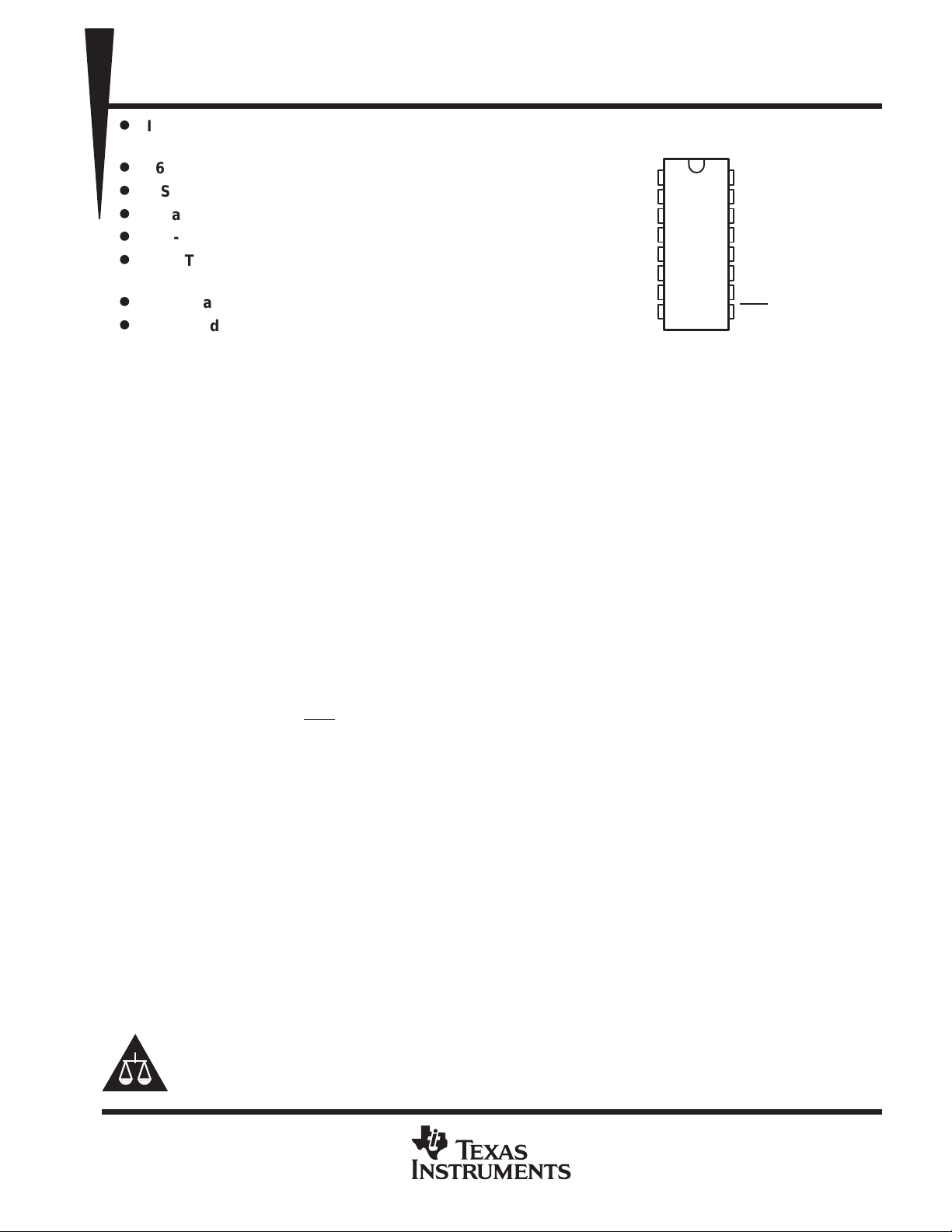
N PACKAGE
(TOP VIEW)
1
16
2
15
3
14
4
13
5
12
6
11
7
10
8
9
V
CC
UNCK
OR
Q0
Q1
Q2
Q3
CLR
D
Independent Synchronous Inputs and
Outputs
D
16 Words by 4 Bits Each
D
3-State Outputs Drive Bus Lines Directly
D
Data Rates up to 10 MHz
D
Fall-Through Time 50 ns Typical
D
Data T erminals Arranged for Printed Circuit
Board Layout
D
Expandable Using External Gating
D
Packaged in Standard Plastic 300-mil DIPs
description
The SN74LS224A 64-bit, low-power Schottky memory is organized as 16 words by 4 bits each. It can be
expanded in multiples of 15m + 1 words or 4n bits, or both (where n is the number of packages in the vertical
array and m is the number of packages in the horizontal array); however, some external gating is required. For
longer words, the input ready (IR) signals of the first-rank packages and output ready (OR) signals of the
last-rank packages must be ANDed for proper synchronization.
A first-in, first-out (FIFO) memory is a storage device that allows data to be written to and read from its array
at independent data rates. These FIFOs are designed to process data at rates up to 10 MHz in a bit-parallel
format, word by word.
The load clock (LDCK) normally is held low, and data is written into memory on the high-to-low transition of
LDCK. The unload clock (UNCK) normally is held high, and data is read out on the low-to-high transition of
UNCK. The memory is full when the number of words clocked in exceeds by 16 the number of words clocked
out. When the memory is full, LDCK signals have no effect on the data residing in memory . When the memory
is empty, UNCK signals have no effect.
Status of the FIFO memory is monitored by the IR and OR flags that indicate not-full and not-empty conditions.
IR is high only when the memory is not full and LDCK is low. OR is high only when the memory is not empty
and UNCK is high.
A low level on the clear (CLR
) input resets the internal stack-control pointers and also sets IR high and OR low
to indicate that old data remaining at the data outputs is invalid. Data outputs are noninverting with respect to
the data inputs and are at high impedance when the output-enable (OE) input is low. OE does not af fect the IR
and OR outputs.
The SN74LS224A is characterized for operation from 0°C to 70°C.
Please be aware that an important notice concerning availability, standard warranty, and use in critical applications of
Texas Instruments semiconductor products and disclaimers thereto appears at the end of this data sheet.
PRODUCTION DATA information is current as of publication date.
Products conform to specifications per the terms of Texas Instruments
standard warranty. Production processing does not necessarily include
testing of all parameters.
POST OFFICE BOX 655303 • DALLAS, TEXAS 75265
Copyright 1999, Texas Instruments Incorporated
1
SN74LS224A
16 × 4 SYNCHRONOUS FIRST -IN, FIRST-OUT MEMORY
WITH 3-STATE OUTPUTS
SDLS023C – JANUARY 1991 – REVISED DECEMBER 1999
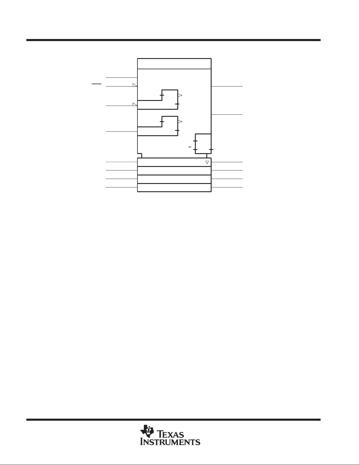
logic symbol
†
This symbol is in accordance with ANSI/IEEE Standard 91-1984 and IEC Publication 617-12. This symbol is functionally accurate but does
not show the details of implementation; for these, see the logic diagram. The symbol represents the memory as if it were controlled by a single
counter whose content is the number of words stored at the time. Output data is invalid when the counter content (CT) is 0.
†
FIFO 16 × 4
OE
CLR
LDCK
UNCK
D0
D1
D2
D3
1
9
3
15
4
5
6
7
EN5
CT = 0
CT < 16
CT > 0
1D
CTR
&
&
+ /C1
Z2
–
Z3
CT = 0
2
14
13
12
11
10
IR
OR
Q0
Q1
Q2
Q3
2
3
&
V4
2
4, 5
2
POST OFFICE BOX 655303 • DALLAS, TEXAS 75265
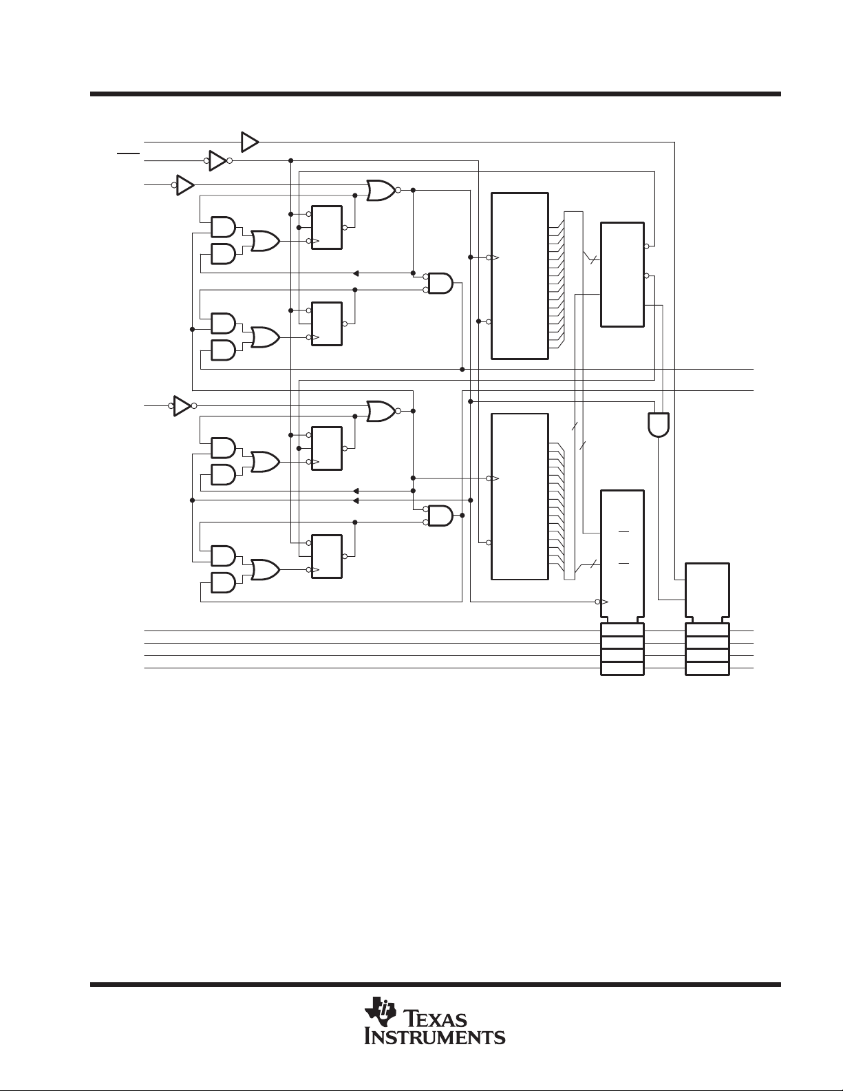
logic diagram (positive logic)
1
OE
9
CLR
3
LDCK
15
UNCK
4
D0
5
D1
6
D2
7
D3
S
1D
S
2D
R
3D
R
4D
C1
C2
C3
C4
SN74LS224A
16 × 4 SYNCHRONOUS FIRST -IN, FIRST-OUT MEMORY
WITH 3-STATE OUTPUTS
SDLS023C – JANUARY 1991 – REVISED DECEMBER 1999
Ring
Counter
CTR
DIV 16
+
Write
Address
CT = 1
Ring
Counter
CTR
DIV 16
+
Read
Address
CT = 1
1
2
3
4
5
6
7
8
9
10
11
12
13
14
15
16
16
1
2
3
4
5
6
7
8
9
10
11
12
13
14
15
16
16
16
16
COMP
Q=P+1
P
P=Q+1
Q
P=Q
EMPTY
RAM
16 × 4
1
1A
16
1
2A
16
C5
1A,5D 2A
EN
2
IR
14
OR
13
≥1
12
11
10
Q0
Q1
Q2
Q3
POST OFFICE BOX 655303 • DALLAS, TEXAS 75265
3

SN74LS224A
16 × 4 SYNCHRONOUS FIRST -IN, FIRST-OUT MEMORY
WITH 3-STATE OUTPUTS
SDLS023C – JANUARY 1991 – REVISED DECEMBER 1999
schematics of inputs and outputs
EQUIVALENT OF CLR
INPUT
V
CC
Input
TYPICAL OF IR
AND OR OUTPUTS
120 Ω NOM
13 kΩ NOM
V
CC
EQUIVALENT OF
OTHER INPUTS
V
CC
Input
TYPICAL OF
Q OUTPUTS
100 Ω NOM
19 kΩ NOM
V
CC
Output
Output
4
POST OFFICE BOX 655303 • DALLAS, TEXAS 75265

IOHHigh-level output current
mA
IOLLow-level output current
mA
timing diagram
CLR
LDCK
UNCK
SN74LS224A
16 × 4 SYNCHRONOUS FIRST -IN, FIRST-OUT MEMORY
WITH 3-STATE OUTPUTS
SDLS023C – JANUARY 1991 – REVISED DECEMBER 1999
D0–D3
IR
OR
Q0–Q3
Invalid Word 1 Word 2 Word 1
W1 W2 W1 W2 W15 W16
Invalid
Load
Two Words
Unload
Two Words
Load Until Full
Word 2
UnloadInitialize
absolute maximum ratings over operating free-air temperature range (unless otherwise noted)
Supply voltage range, VCC (see Note 1) –0.5 V to 7 V. . . . . . . . . . . . . . . . . . . . . . . . . . . . . . . . . . . . . . . . . . . . . .
Input voltage range, VI –0.5 V to 7 V. . . . . . . . . . . . . . . . . . . . . . . . . . . . . . . . . . . . . . . . . . . . . . . . . . . . . . . . . . . . . .
Off-state output voltage range, V
Package thermal impedance, θJA (see Note 2) 78°C/W. . . . . . . . . . . . . . . . . . . . . . . . . . . . . . . . . . . . . . . . . . . . .
Storage temperature range, T
†
Stresses beyond those listed under “absolute maximum ratings” may cause permanent damage to the device. These are stress ratings only and
functional operation of the device at these or any other conditions beyond those indicated under “recommended operating conditions” is not
implied. Exposure to absolute-maximum-rated conditions for extended periods may affect device reliability.
NOTES: 1. All voltage values are with respect to GND.
2. The package thermal impedance is calculated in accordance with JESD 51.
–0.5 V to 5.5 V. . . . . . . . . . . . . . . . . . . . . . . . . . . . . . . . . . . . . . . . . . . . . . . . . .
O
–65°C to 150°C. . . . . . . . . . . . . . . . . . . . . . . . . . . . . . . . . . . . . . . . . . . . . . . . . . .
stg
†
recommended operating conditions (see Note 3)
V
CC
V
IH
V
IL
T
A
NOTE 3: To ensure proper operation of this high-speed FIFO device, it is necessary to provide a clean signal to the LDCK and UNCK clock inputs.
MIN NOM MAX UNIT
Supply voltage 4.75 5 5.25 V
High-level input voltage 2 V
Low-level input voltage 0.8 V
p
p
Operating free-air temperature 0 70 °C
Any excessive noise or glitching on the clock inputs that violates the VIL, VIH, or minimum pulse-duration limits can cause a false clock
or improper operation of the internal read and write pointers.
POST OFFICE BOX 655303 • DALLAS, TEXAS 75265
Q outputs –2.6
IR, OR –0.4
Q outputs 24
IR, OR 8
5

SN74LS224A
V
V
Q outputs
V
4.75 V
V
V
IR, OR
V
4.75 V
I
‡
V
V
mA
16 × 4 SYNCHRONOUS FIRST -IN, FIRST-OUT MEMORY
WITH 3-STATE OUTPUTS
SDLS023C – JANUARY 1991 – REVISED DECEMBER 1999
electrical characteristics over recommended operating free-air temperature range (unless
otherwise noted)
PARAMETER
V
IK
Q outputs VCC = 4.75 V, IOH = –2.6 mA 2.4 3.4
OH
IR, OR VCC = 4.75 V, IOH = –0.4 mA 2.7 3.4
p
OL
I
OZH
I
OZL
I
I
I
IH
I
IL
OS
I
CC
†
All typical values are at VCC = 5 V, TA = 25°C.
‡
Not more than one output should be shorted at a time, and duration of the short circuit should not exceed one second.
Q outputs VCC = 5.25 V, VO = 2.7 V 20 µA
Q outputs VCC = 5.25 V, VO = 0.4 V –20 µA
Q outputs
IR, OR
VCC = 4.75 V, II = –18 mA –1.5 V
=
CC
=
CC
VCC = 5.25 V, VI = 7 V 0.1 mA
VCC = 5.25 V, VI = 2.7 V 20 µA
VCC = 5.25 V, VI = 0.4 V –0.4 mA
= 5.25
CC
VCC = 5.25 V
TEST CONDITIONS
IOL = 12 mA 0.25 0.4
IOL = 24 mA 0.35 0.5
IOL = 4 mA 0.25 0.4
IOL = 8 mA 0.35 0.5
Outputs high 84 135
Outputs low 87 155
Outputs disabled 89 155
MIN TYP†MAX UNIT
–30 –130
–20 –100
mA
timing requirements over recommended operating conditions (see Note 3 and Figure 1)
MIN NOM MAX UNIT
LDCK high 60
LDCK low 15
t
w
t
su
t
h
NOTE 3: To ensure proper operation of this high-speed FIFO device, it is necessary to provide a clean signal to the LDCK and UNCK clock inputs.
Pulse duration
Setup time
Hold time Data from LDCK↓ 10 ns
Any excessive noise or glitching on the clock inputs that violates the VIL, VIH, or minimum pulse-duration limits can cause a false clock
or improper operation of the internal read and write pointers.
UNCK low
UNCK high 30
CLR low 20
Data to LDCK↓ 50
LDCK↓ before UNCK↓
UNCK↑ before LDCK↑ 50
30
50
ns
ns
6
POST OFFICE BOX 655303 • DALLAS, TEXAS 75265

IR
R
C
pF
ns
OR
R
C
pF
ns
IR
R
C
pF
ns
OR
R
C
pF
ns
PLH
CLR↓
R
C
pF
ns
PLH
UNCK↑
Q
R
667 Ω
C
pF
ns
OE↑
Q
R
667 Ω
C
pF
ns
OE↓
Q
R
667 Ω
C
pF
16 × 4 SYNCHRONOUS FIRST -IN, FIRST-OUT MEMORY
switching characteristics, VCC = 5 V, TA = 25°C (see Figure 1)
PARAMETER
t
PLH
t
PHL
t
PLH
t
PHL
t
PLH
t
PHL
t
PLH
t
PLH
t
PHL
t
PLH
t
t
PHL
t
PHL
t
t
PHL
t
PZL
t
PZH
t
PLZ
t
PHZ
FROM
(INPUT)
IRE↑
IRE↓
ORE↑
ORE↓
LDCK↓
LDCK↑
LDCK↓ OR RL = 2 kΩ, CL = 15 pF 48 70 ns
UNCK↑
UNCK↓
UNCK↑ IR RL = 2 kΩ, CL = 15 pF 49 70 ns
LDCK↓ Q RL = 667 Ω, CL = 45 pF 34 50 ns
TO
(OUTPUT)
IR
OR
L
L
L
L
L
L
L
L
SN74LS224A
WITH 3-STATE OUTPUTS
SDLS023C – JANUARY 1991 – REVISED DECEMBER 1999
CONDITIONS
= 2 kΩ,
= 2 kΩ,
= 2 kΩ,
= 2 kΩ,
= 2 kΩ,
=
=
=
TEST
,
,
,
= 15
L
= 15
L
= 15
L
= 15
L
= 15
L
= 45
L
= 45
L
= 5
L
p
p
p
p
p
p
p
p
TYP MAX UNIT
N/A N/A
N/A N/A
N/A N/A
N/A N/A
25 40
36 50
29 45
28 45
36 55
25 40
54 80
45 70
22 35
21 35
16 30 ns
18 30 ns
POST OFFICE BOX 655303 • DALLAS, TEXAS 75265
7

SN74LS224A
16 × 4 SYNCHRONOUS FIRST -IN, FIRST-OUT MEMORY
WITH 3-STATE OUTPUTS
SDLS023C – JANUARY 1991 – REVISED DECEMBER 1999
PARAMETER MEASUREMENT INFORMATION
V
CC
R
L
From Output
Under Test
(see Note A)
Timing
Input
Data
Input
Output
Control
(low-level
enabling)
Waveform 1
(see Note B)
Waveform 2
(see Note B)
ENABLE AND DISABLE TIMES, 3-STATE OUTPUTS
NOTES: A. CL includes probe and jig capacitance.
B. Waveform 1 is for an output with internal conditions such that the output is low except when disabled by the output control.
Waveform 2 is for an output with internal conditions such that the output is high except when disabled by the output control.
C. All input pulses have the following characteristics: PRR ≤ 1 MHz, tr < 15 ns, tf < 6 ns, ZO ≈ 50 Ω.
D. All diodes are 1N916 or 1N3064.
E. The outputs are measured one at a time with one transition per measurement.
C
L
LOAD CIRCUIT
t
su
VOLTAGE WAVEFORMS
SETUP AND HOLD TIMES
t
PZL
1.3 V
t
t
PZH
VOLTAGE WAVEFORMS
PHZ
1.3 V
1.3 V
5 kΩ
t
h
1.3 V1.3 V
1.3 V1.3 V
S1
(see Note B)
S2
3 V
0 V
3 V
0 V
t
PLZ
0.5 V
3 V
0 V
[
V
0.5 V
V
[
1.5 V
OL
OH
1.5 V
t
PLZ/tPHZ
t
PLH/tPHL
High-Level
Pulse
Low-Level
Pulse
Output
Control
In-Phase
Output
Out-of-Phase
Output
(see Note C)
TEST S1
t
PZL
t
PZH
VOLTAGE WAVEFORMS
t
PLH
t
PHL
VOLTAGE WAVEFORMS
PROPAGATION DELAY TIMES
Closed
Open
Closed
Closed
1.3 V 1.3 V
t
w
1.3 V 1.3 V
PULSE DURATIONS
1.3 V 1.3 V
1.3 V 1.3 V
S2
Open
Closed
Closed
Closed
1.3 V1.3 V
t
t
PHL
PLH
3 V
0.3 V
V
OH
V
OL
V
OH
V
OL
Figure 1. Load Circuits and Voltage Waveforms
8
POST OFFICE BOX 655303 • DALLAS, TEXAS 75265

IMPORTANT NOTICE
T exas Instruments and its subsidiaries (TI) reserve the right to make changes to their products or to discontinue
any product or service without notice, and advise customers to obtain the latest version of relevant information
to verify, before placing orders, that information being relied on is current and complete. All products are sold
subject to the terms and conditions of sale supplied at the time of order acknowledgement, including those
pertaining to warranty, patent infringement, and limitation of liability.
TI warrants performance of its semiconductor products to the specifications applicable at the time of sale in
accordance with TI’s standard warranty. Testing and other quality control techniques are utilized to the extent
TI deems necessary to support this warranty . Specific testing of all parameters of each device is not necessarily
performed, except those mandated by government requirements.
CERTAIN APPLICATIONS USING SEMICONDUCTOR PRODUCTS MAY INVOLVE POTENTIAL RISKS OF
DEATH, PERSONAL INJURY, OR SEVERE PROPERTY OR ENVIRONMENTAL DAMAGE (“CRITICAL
APPLICATIONS”). TI SEMICONDUCTOR PRODUCTS ARE NOT DESIGNED, AUTHORIZED, OR
WARRANTED TO BE SUITABLE FOR USE IN LIFE-SUPPORT DEVICES OR SYSTEMS OR OTHER
CRITICAL APPLICA TIONS. INCLUSION OF TI PRODUCTS IN SUCH APPLICATIONS IS UNDERST OOD TO
BE FULLY AT THE CUSTOMER’S RISK.
In order to minimize risks associated with the customer’s applications, adequate design and operating
safeguards must be provided by the customer to minimize inherent or procedural hazards.
TI assumes no liability for applications assistance or customer product design. TI does not warrant or represent
that any license, either express or implied, is granted under any patent right, copyright, mask work right, or other
intellectual property right of TI covering or relating to any combination, machine, or process in which such
semiconductor products or services might be or are used. TI’s publication of information regarding any third
party’s products or services does not constitute TI’s approval, warranty or endorsement thereof.
Copyright 1999, Texas Instruments Incorporated
 Loading...