

Datasheet JM38510-31402B2A, JM38510-31402BFA, JM38510-31402BEA, SN54221J, SN54LS221J Datasheet (Texas Instruments)
...Page 1
SN54221, SN54LS221, SN74221, SN74LS221
DUAL MONOSTABLE MULTIVIBRATORS
WITH SCHMITT-TRIGGER INPUTS
SDLS213A – DECEMBER 1983 – REVISED FEBRUARY 1998
D
Dual Versions of Highly Stable SN54121
and SN74121 One Shots
D
SN54221 and SN74221 Demonstrate
Electrical and Switching Characteristics
That Are Virtually Identical to the SN54121
and SN74121 One Shots
D
Pinout Is Identical to the SN54123,
SN74123, SN54LS123, and SN74LS123
D
Overriding Clear Terminates Output Pulse
D
Package Options Include Plastic
Small-Outline (D), Shrink Small-Outline
(DB) Packages, Ceramic Chip Carriers (FK)
and Flat Packs (W), and Standard Plastic
(N) and Ceramic (J) 300-mil DIPs
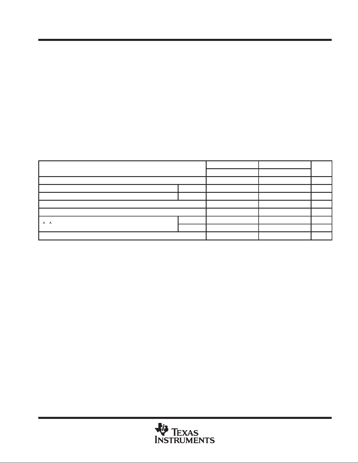
MAXIMUM
OUTPUT
TYPE
SN54221 21
SN74221 28
SN54LS221 49
SN74LS221 70
PULSE
LENGTH(S)
description
The ’221 and ’LS221 devices are monolithic dual
multivibrators with performance characteristics
virtually identical to those of the ’121 devices.
Each multivibrator features a negative-transitiontriggered input and a positive-transition-triggered
input, either of which can be used as an inhibit
input.
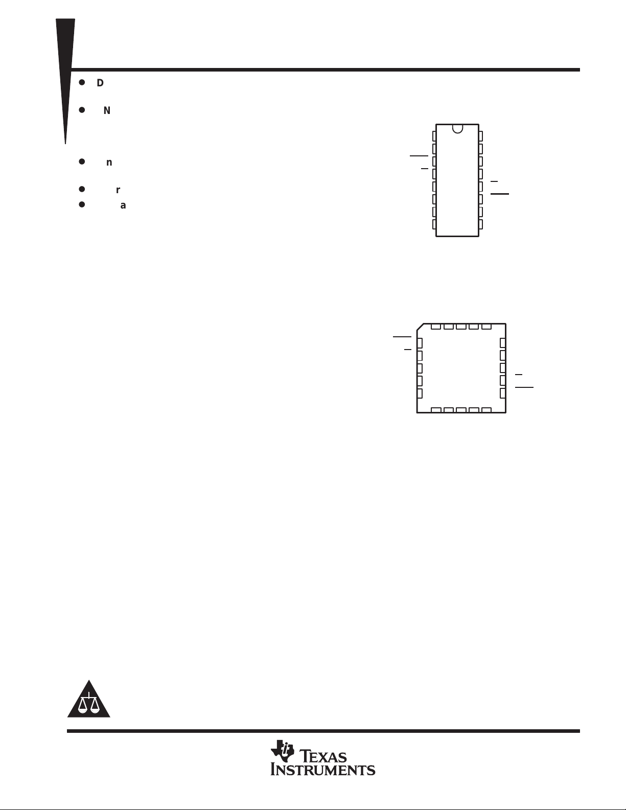
SN54221, SN54LS221 ...J OR W PACKAGE
SN74221 ...N PACKAGE
SN74LS221 . . . D, DB, OR N PACKAGE
2R
ext/Cext
SN54LS221 . . . FK PACKAGE
1A
1B
1CLR
1Q
2Q
2C
ext
GND
(TOP VIEW)
1
16
2
15
3
14
4
13
5
12
6
11
7
10
8
(TOP VIEW)
9
V
CC
1R
ext/Cext
1C
ext
1Q
2Q
2CLR
2B
2A
ext
/C
ext
GND
NC
CC
V
2A
1R
18
17
16
15
14
2B
1C
ext
1Q
NC
2Q
2CLR
1CLR
1Q
NC
2Q
2C
ext
1B1ANC
3212019
4
5
6
7
8
9
10 11 12 13
ext
ext
2R /C
NC – No internal connection
Pulse triggering occurs at a particular voltage level and is not directly related to the transition time of the input
pulse. Schmitt-trigger input circuitry (TTL hysteresis) for B input allows jitter-free triggering from inputs with
transition rates as slow as 1 V/s, providing the circuit with excellent noise immunity, typically of 1.2 V. A high
immunity to V
noise, typically of 1.5 V, is also provided by internal latching circuitry.
CC
Once fired, the outputs are independent of further transitions of the A and B inputs and are a function of the timing
components, or the output pulses can be terminated by the overriding clear. Input pulses can be of any duration
relative to the output pulse. Output pulse length can be varied from 35 ns to the maximums shown in the above
table by choosing appropriate timing components. With R
= 2 kΩ and C
ext
= 0, an output pulse typically of
ext
30 ns is achieved, which can be used as a dc-triggered reset signal. Output rise and fall times are TTL
compatible and independent of pulse length. Typical triggering and clearing sequences are shown as a part of
the switching characteristics waveforms.
Pulse-width stability is achieved through internal compensation and is virtually independent of VCC and
temperature. In most applications, pulse stability is limited only by the accuracy of external timing components.
Please be aware that an important notice concerning availability, standard warranty, and use in critical applications of
Texas Instruments semiconductor products and disclaimers thereto appears at the end of this data sheet.
PRODUCTION DATA information is current as of publication date.
Products conform to specifications per the terms of Texas Instruments
standard warranty. Production processing does not necessarily include
testing of all parameters.
POST OFFICE BOX 655303 • DALLAS, TEXAS 75265
Copyright 1998, Texas Instruments Incorporated
On products compliant to MIL-PRF-38535, all parameters are tested
unless otherwise noted. On all other products, production
processing does not necessarily include testing of all parameters.
1
Page 2
SN54221, SN54LS221, SN74221, SN74LS221
DUAL MONOSTABLE MULTIVIBRATORS
WITH SCHMITT-TRIGGER INPUTS
SDLS213A – DECEMBER 1983 – REVISED FEBRUARY 1998
description (continued)
Jitter-free operation is maintained over the full temperature and VCC ranges for more than six decades of timing
capacitance (10 pF to 10 µF) and more than one decade of timing resistance (2 kΩ to 30 kΩ for the SN54221,
2 kΩ to 40 kΩ for the SN74221, 2 kΩ to 70 kΩ for the SN54LS221, and 2 kΩ to 100 kΩ for the SN74LS221).
Throughout these ranges, pulse width is defined by the relationship: t
circuits where pulse cutoff is not critical, timing capacitance up to 1000 µF and timing resistance as low as 1.4 kΩ
can be used. Also, the range of jitter-free output pulse widths is extended if VCC is held to 5 V and free-air
temperature is 25°C. Duty cycles as high as 90% are achieved when using maximum recommended RT. Higher
duty cycles are available if a certain amount of pulse-width jitter is allowed.
The variance in output pulse width from device to device typically is less than ±0.5% for given external timing
components. An example of this distribution for the ’221 is shown in Figure 3. V ariations in output pulse width
versus supply voltage and temperature for the ’221 are shown in Figures 4 and 5, respectively.
Pin assignments for these devices are identical to those of the SN54123/SN74123 or SN54LS123/SN74LS123
so that the ’221 or ’LS221 devices can be substituted for those products in systems not using the retrigger by
merely changing the value of R
and/or C
ext
; however, the polarity of the capacitor must be changed.
ext
The SN54221 and SN54LS221 are characterized for operation over the full military temperature range of –55°C
to 125°C. The SN74221 and SN74LS221 are characterized for operation from 0°C to 70°C.
(out) = C
w
extRext
In2 ≈ 0.7 C
extRext
. In
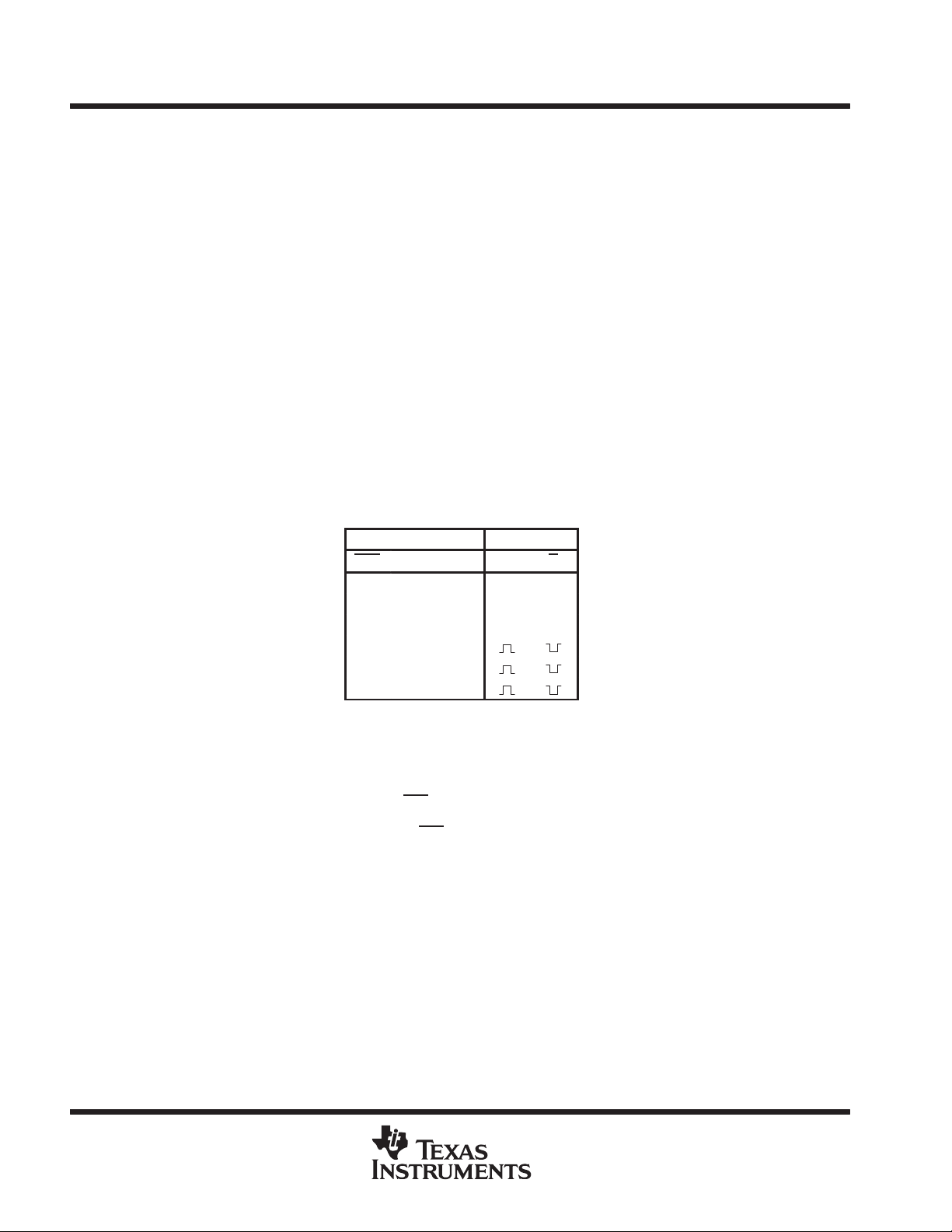
FUNCTION TABLE
(each monostable multivibrator)
INPUTS OUTPUTS
CLR A B Q Q
L X X L H
X HXLH
X XLLH
H L ↑
H ↓ H
‡
↑
†
Pulsed-output patterns are tested during
AC switching at 25°C with R
C
ext
‡
This condition is true only if the output of
the latch formed by the two NAND gates
has been conditioned to the logic 1 state
prior to CLR
conditioned by taking either A high or
B low while CLR
L H
= 80 pF.
going high. This latch is
is inactive (high).
†
†
† †
= 2 kΩ, and
ext
†
†
2
POST OFFICE BOX 655303 • DALLAS, TEXAS 75265
Page 3
SN54221, SN54LS221, SN74221, SN74LS221
DUAL MONOSTABLE MULTIVIBRATORS
WITH SCHMITT-TRIGGER INPUTS
SDLS213A – DECEMBER 1983 – REVISED FEBRUARY 1998
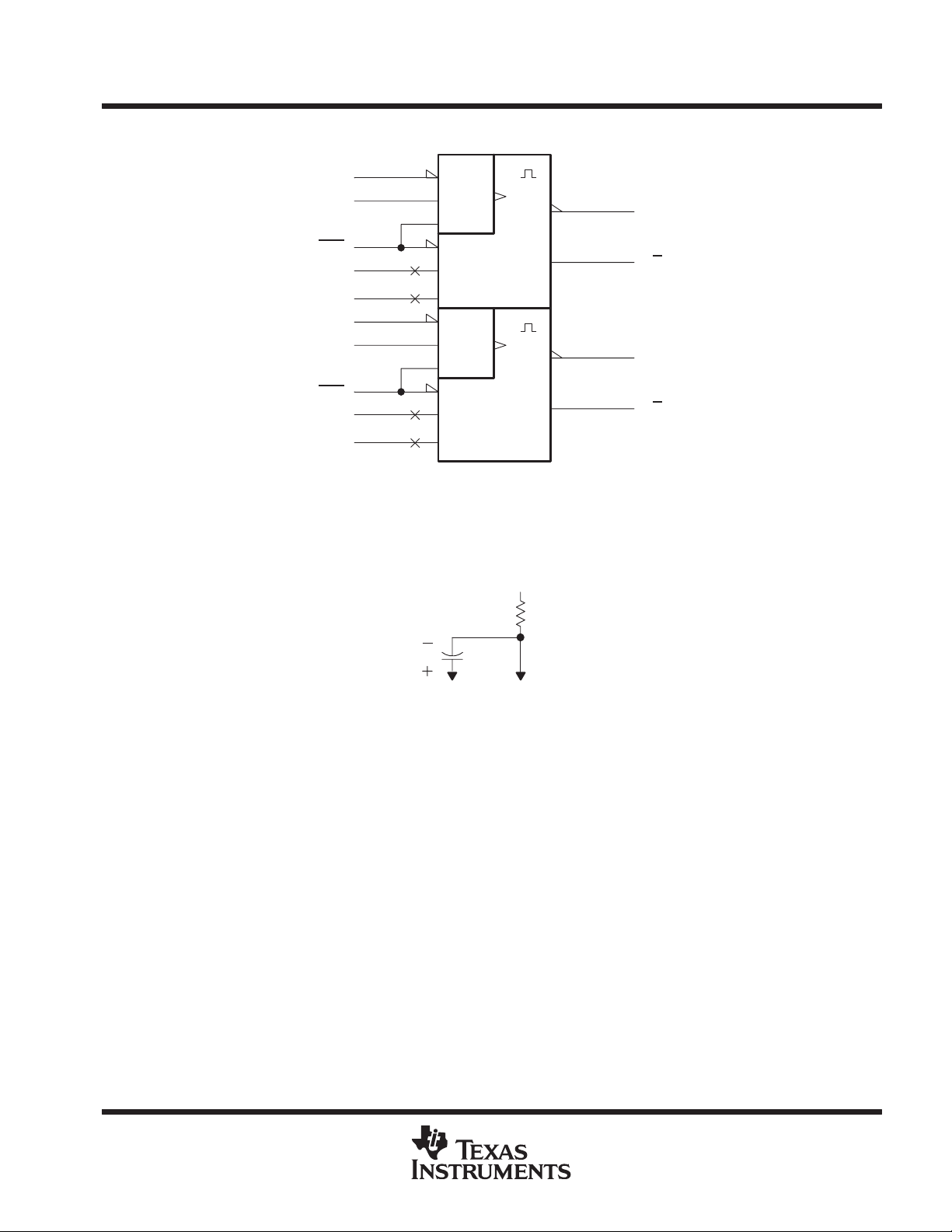
logic symbol
†
This symbol is in accordance with ANSI/IEEE Std 91-1984 and IEC Publication 617-12.
Pin numbers shown are for the D, DB, J, N, and W packages.
†
1R
ext/Cext
2R
ext/Cext
1A
1B
1CLR
1C
ext
2A
2B
2CLR
2C
ext
1
2
3
14
15
9
10
11
6
7
&
R
CX
RX/CX
&
R
CX
RX/CX
1
1
timing component connections
13
12
1Q
4
1Q
5
2Q
2Q
NOTE: Due to the internal circuit, the R
To C
Terminal
terminal is never more positive than the C
ext/Cext
ext
To R
V
CC
R
ext/Cext
Terminal
ext
terminal.
ext
POST OFFICE BOX 655303 • DALLAS, TEXAS 75265
3
Page 4
SN54221, SN54LS221, SN74221, SN74LS221
DUAL MONOSTABLE MULTIVIBRATORS
WITH SCHMITT-TRIGGER INPUTS
SDLS213A – DECEMBER 1983 – REVISED FEBRUARY 1998
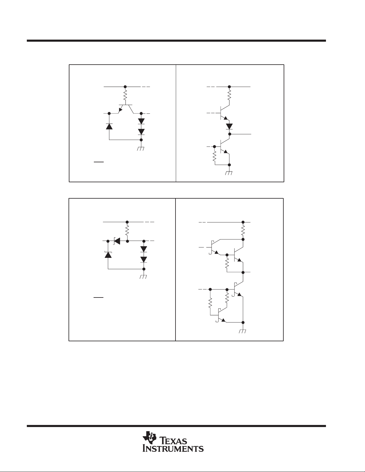
schematics of inputs and outputs
SN54/74221
EQUIVALENT OF EACH INPUT TYPICAL OF ALL OUTPUTS
V
CC
R
eq
Input
A Input: Req = 4 kΩ NOM
Input: Req = 2 kΩ NOM
B, CLR
SN54/74LS221
EQUIVALENT OF EACH INPUT TYPICAL OF ALL OUTPUTS
V
CC
R
eq
Input
100 Ω NOM
120 Ω NOM
V
CC
Output
V
CC
A Input: Req = 25 kΩ NOM
B Input: Req = 15.4 kΩ NOM
CLR
: Req = 12.5 kΩ NOM
Output
4
POST OFFICE BOX 655303 • DALLAS, TEXAS 75265
Page 5
UNIT
∆v/∆t
Rise or fall of input pulse rate
SN54221, SN54LS221, SN74221, SN74LS221
DUAL MONOSTABLE MULTIVIBRATORS
WITH SCHMITT-TRIGGER INPUTS
SDLS213A – DECEMBER 1983 – REVISED FEBRUARY 1998
absolute maximum ratings over operating free-air temperature range (unless otherwise noted)
Supply voltage range, V
Input voltage range, VI (see Note 1): ’LS221 7 V. . . . . . . . . . . . . . . . . . . . . . . . . . . . . . . . . . . . . . . . . . . . . . . . . . .
Package thermal impedance, θJA (see Note 2): D package 113°C/W. . . . . . . . . . . . . . . . . . . . . . . . . . . . . . . . . .
Storage temperature range, T
†
Stresses beyond those listed under “absolute maximum ratings” may cause permanent damage to the device. These are stress ratings only, and
functional operation of the device at these or any other conditions beyond those indicated under “recommended operating conditions” is not
implied. Exposure to absolute-maximum-rated conditions for extended periods may affect device reliability.
NOTES: 1. The input and output negative-voltage ratings may be exceeded if the input and output clamp-current ratings are observed.
2. The package thermal impedance is calculated in accordance with JESD 51, except for through-hole packages, which use a trace
length of zero
7 V. . . . . . . . . . . . . . . . . . . . . . . . . . . . . . . . . . . . . . . . . . . . . . . . . . . . . . . . . . . . . . . . . . .
CC
’221 5.5 V. . . . . . . . . . . . . . . . . . . . . . . . . . . . . . . . . . . . . . . . . . . . . . . . . . . .
DB package 131°C/W. . . . . . . . . . . . . . . . . . . . . . . . . . . . . . . .
N package 78°C/W. . . . . . . . . . . . . . . . . . . . . . . . . . . . . . . . . . .
–65°C to 150°C. . . . . . . . . . . . . . . . . . . . . . . . . . . . . . . . . . . . . . . . . . . . . . . . . . .
stg
recommended operating conditions
SN54221 SN74221
MIN NOM MAX MIN NOM MAX
V
V
V
I
OH
I
OL
T
∗ On products compliant to MIL-PRF-38535, this parameter is not production tested.
Supply voltage 4.5 5 5.5 4.75 5 5.25 V
CC
High-level input voltage A input 2 2 V
IH
Low-level input voltage A input 0.8 0.8 V
IL
High-level output current –800 –800 µA
Low-level output current 16 16 mA
p
p
Operating free-air temperature –55 125 0 70 °C
A
B input 1* 1 V/s
A input 1* 1 V/µs
†
POST OFFICE BOX 655303 • DALLAS, TEXAS 75265
5
Page 6

SN54221, SN54LS221, SN74221, SN74LS221
PARAMETER
TEST CONDITIONS
†
UNIT
I
V
MAX
V
2.4 V
A
I
V
MAX
V
V
mA
I
V
MAX
mA
UNIT
twPulse duration
ns
Output duty cycle
DUAL MONOSTABLE MULTIVIBRATORS
WITH SCHMITT-TRIGGER INPUTS
SDLS213A – DECEMBER 1983 – REVISED FEBRUARY 1998
electrical characteristics over recommended operating free-air temperature range (unless
otherwise noted)
SN54221 SN74221
MIN TYP‡MAX MIN TYP‡MAX
Positive-going threshold voltage,
V
T+
B input
Negative-going threshold voltage,
V
T–
B input
V
IK
V
OH
V
OL
I
I
A input
IH
CLR, B input
A input
IL
CLR, B input
§
I
OS
Quiescent
CC
Triggered
∗ On products compliant to MIL-PRF-38535, this parameter is not production tested.
†
For conditions shown as MIN or MAX, use the appropriate value specified under recommended operating conditions.
‡
All typical values are at VCC = 5 V, TA = 25°C.
§
Not more than one output should be shorted at a time and the duration of the short circuit should not exceed one second.
VCC = MIN 1.55 2* 1.55 2 V
VCC = MIN 0.8* 1.35 0.8 1.35 V
VCC = MIN, II = –12 mA –1.5 –1.5 V
VCC = MIN, IOH = –800 µA 2.4 3.4 2.4 3.4 V
VCC = MIN, IOL = 16 mA 0.2 0.4 0.2 0.4 V
VCC = MAX, VI = 5.5 V 1 1 mA
,
=
CC
=
CC
VCC = MAX –20 –55 –18 –55 mA
=
CC
=
I
,
= 0.4
I
26 50* 26 50
46 80* 46 80
40 40
80 80
–1.6 –1.6
–3.2 –3.2
µ
timing requirements over recommended ranges of supply voltage and operating free-air
temperature
SN54221 SN74221
MIN MAX MIN MAX
A or B input 50 50
CLR 20 20
t
su
R
C
∗ On products compliant to MIL-PRF-38535, this parameter is not production tested.
¶
Inactive-state setup time is also referred to as recovery time.
Setup time, inactive-state¶
External timing resistance
ext
External timing capacitance
ext
p
CLR 15 15 ns
1.4* 30* 1.4 40 kΩ
0* 1000* 0 1000 µF
R
= 2 kΩ 67% 67%
ext
R
= MAX R
ext
ext
90% 90%
6
POST OFFICE BOX 655303 • DALLAS, TEXAS 75265
Page 7

PARAMETER
TEST CONDITIONS
UNIT
t
Q
C
R
kΩ
ns
t
Q
CLR
C
R
kΩ
ns
t
A or B
Q or Q
UNIT
∆v/∆t
Rise or fall of input pulse rate
SN54221, SN54LS221, SN74221, SN74LS221
DUAL MONOSTABLE MULTIVIBRATORS
WITH SCHMITT-TRIGGER INPUTS
SDLS213A – DECEMBER 1983 – REVISED FEBRUARY 1998
switching characteristics VCC = 5 V, RL = 400 Ω, TA = 25_C (see Figures 1 and 2)
FROM TO
(INPUT) (OUTPUT)
PLH
PHL
t
PHL
t
PLH
w
∗ On products compliant to MIL-PRF-38535, this parameter is not production tested.
A
B
A
B
Q
Q
= 80 pF,
ext
= 80 pF,
ext
C
= 80 pF, R
ext
C
= 0, R
ext
C
= 100 pF, R
ext
C
= 1 µF, R
ext
= 2
ext
= 2
ext
= 2 kΩ
ext
= 2 kΩ
ext
= 10 kΩ
ext
= 10 kΩ
ext
recommended operating conditions
V
V
V
I
OH
I
OL
T
∗ On products compliant to MIL-PRF-38535, this parameter is not production tested.
Supply voltage 4.5 5 5.5 4.75 5 5.25 V
CC
High-level input voltage A input 2 2 V
IH
Low-level input voltage A input 0.7 0.8 V
IL
High-level output current –400 –400 µA
Low-level output current 4 8 mA
p
p
Operating free-air temperature –55 125 0 70 °C
A
B input 1
A input 1
SN54221 SN74221
MIN TYP MAX MIN TYP MAX
45 70 45 70
35 55 35 55
50 80 50 80
40 65 40 65
27 27
40 40
70 110 150 70 110 150
17 30 50 17 30 50
650 700 750 650 700 750
6.5* 7 7.5* 6.5 7 7.5 ms
SN54LS221 SN74LS221
MIN NOM MAX MIN NOM MAX
*
*
1 V/s
1 V/µs
ns
POST OFFICE BOX 655303 • DALLAS, TEXAS 75265
7
Page 8

SN54221, SN54LS221, SN74221, SN74LS221
PARAMETER
TEST CONDITIONS
†
UNIT
VOLV
MIN
V
I
V
MAX
V
V
mA
I
V
MAX
mA
UNIT
twPulse duration
ns
Output duty cycle
DUAL MONOSTABLE MULTIVIBRATORS
WITH SCHMITT-TRIGGER INPUTS
SDLS213A – DECEMBER 1983 – REVISED FEBRUARY 1998
electrical characteristics over recommended operating free-air temperature range (unless
otherwise noted)
SN54LS221 SN74LS221
MIN TYP‡MAX MIN TYP‡MAX
Positive-going threshold voltage,
V
T+
B input
Negative-going threshold voltage,
V
T–
B input
V
IK
V
OH
I
I
I
IH
A input
IL
CLR, B input
§
I
OS
Quiescent
CC
Triggered
∗ On products compliant to MIL-PRF-38535, this parameter is not production tested.
†
For conditions shown as MIN or MAX, use the appropriate value specified under recommended operating conditions.
‡
All typical values are at VCC = 5 V, TA = 25°C.
§
Not more than one output should be shorted at a time and the duration of the short circuit should not exceed one second.
VCC = MIN 1 2* 1 2 V
VCC = MIN 0.7* 0.9 0.8 0.9 V
VCC = MIN, II = –18 mA –1.5 –1.5 V
VCC = MIN, IOH = –400 µA 2.5 3.4 2.7 3.4 V
=
CC
VCC = MAX, VI = 7 V 0.1 0.1 mA
VCC = MAX, VI = 2.7 V 20 20 µA
=
CC
VCC = MAX –20 –100 –20 –100 mA
=
CC
IOL = 4 mA 0.25 0.4 0.25 0.4
IOL = 8 mA 0.35 0.5
,
= 0.4
I
–0.4 –0.4
–0.8 –0.8
4.7 11 4.7 11
19 27* 19 27
timing requirements over recommended ranges of supply voltage and operating free-air
temperature
SN54LS221 SN74LS221
MIN MAX MIN MAX
A or B 50 50
CLR 40 40
t
su
R
C
∗ On products compliant to MIL-PRF-38535, this parameter is not production tested.
¶
Inactive-state setup time is also referred to as recovery time.
Setup time, inactive state
External timing resistance
ext
External timing capacitance
ext
p
¶
CLR 15 15 ns
1.4* 70* 1.4 100 kΩ
0* 1000* 0 1000 µF
RT = 2 kΩ 50% 50%
RT = MAX R
ext
90% 90%
8
POST OFFICE BOX 655303 • DALLAS, TEXAS 75265
Page 9

PARAMETER
TEST CONDITIONS
UNIT
t
Q
C
R
kΩ
ns
t
Q
CLR
C
R
kΩ
ns
t
A or B
Q or Q
SN54221, SN54LS221, SN74221, SN74LS221
DUAL MONOSTABLE MULTIVIBRATORS
WITH SCHMITT-TRIGGER INPUTS
SDLS213A – DECEMBER 1983 – REVISED FEBRUARY 1998
switching characteristics VCC = 5 V, RL = 2 kΩ, TA = 25_C (see Figures 1 and 2)
FROM TO
(INPUT) (OUTPUT)
PLH
PHL
t
PHL
t
PLH
w
∗ On products compliant to MIL-PRF-38535, this parameter is not production tested.
A
B
A
B
Q
Q
= 80 pF,
ext
= 80 pF,
ext
C
= 80 pF, R
ext
C
= 0, R
ext
C
= 100 pF, R
ext
C
= 1 µF, R
ext
= 2
ext
= 2
ext
= 2 kΩ
ext
= 2 kΩ
ext
= 10 kΩ
ext
= 10 kΩ
ext
SN54LS221 SN74LS221
MIN TYP MAX MIN TYP MAX
45 70 45 70
35 55 35 55
50 80 50 80
40 65 40 65
35 55 35 55
44 65 44 65
70 120 150 70 120 150
20 47 70 20 47 70
670 740 810 670 740 810
6* 6.9 7.5* 6 6.9 7.5 ms
ns
POST OFFICE BOX 655303 • DALLAS, TEXAS 75265
9
Page 10

SN54221, SN54LS221, SN74221, SN74LS221
DUAL MONOSTABLE MULTIVIBRATORS
WITH SCHMITT-TRIGGER INPUTS
SDLS213A – DECEMBER 1983 – REVISED FEBRUARY 1998
PARAMETER MEASUREMENT INFORMATION
t
w
†
B
≥ 60 ns
CLR
t
PLH
Q
t
PHL
Q
CONDITION 1: TRIGGER FROM B, THEN CLR
t
PHL
t
PLH
3 V
0 V
3 V
0 V
V
V
V
V
OH
OL
OH
OL
†
A is low.
B
CLR
B
CLR
†
Q
†
Triggered
Q
Not Triggered
≥ 60 ns
CONDITION 2: TRIGGER FROM B, THEN CLR
≥ 50 ns
CONDITION 3: CLR
t
≥ 0
OVERRIDING B, THEN TRIGGER FROM B
su
t
w
3 V
0 V
3 V
0 V
V
V
3 V
0 V
3 V
0 V
V
V
OH
OL
OH
OL
10
Figure 1. Switching Characteristics
POST OFFICE BOX 655303 • DALLAS, TEXAS 75265
Page 11

SN54221, SN54LS221, SN74221, SN74LS221
DUAL MONOSTABLE MULTIVIBRATORS
WITH SCHMITT-TRIGGER INPUTS
SDLS213A – DECEMBER 1983 – REVISED FEBRUARY 1998
PARAMETER MEASUREMENT INFORMATION
B
CLR
A
CLR
†
≥ 50 ns
Q
CONDITION 4: TRIGGERING FROM POSITIVE TRANSITION OF CLR
t
w
‡
≥ 60 ns
t
PLH
Q
t
PHL
Q
≥ 50 ns
t
PHL
t
PLH
3 V
0 V
3 V
0 V
V
V
3 V
0 V
3 V
0 V
V
V
V
V
OH
OL
OH
OL
OH
OL
CONDITION 5: TRIGGER FROM A, THEN CLR
‡
A
t
w
Q
t
w
Q
†
A is low.
‡
B and CLR
NOTES: A. Input pulses are supplied by generators having the following characteristics: PRR ≤ 1 MHz, ZO ≈ 50Ω; for SN54/74221, tr ≤ 7 ns,
are high.
tf ≤ 7 ns, for SN54/74LS221, tr ≤ 15 ns, tf ≤ 6 ns.
B. All measurements are made between the 1.5-V points of the indicated transitions for the SN54/74221 or between the 1.3-V points
for the SN54/74LS221.
CONDITION 6: TRIGGER FROM A
3 V
0 V
V
V
V
V
OH
OL
OH
OL
Figure 1. Switching Characteristics (Continued)
POST OFFICE BOX 655303 • DALLAS, TEXAS 75265
11
Page 12

SN54221, SN54LS221, SN74221, SN74LS221
DUAL MONOSTABLE MULTIVIBRATORS
WITH SCHMITT-TRIGGER INPUTS
SDLS213A – DECEMBER 1983 – REVISED FEBRUARY 1998
PARAMETER MEASUREMENT INFORMATION
V
Test
Point
CC
R
L
From Output
Under Test
Timing
Input
Data
Input
CL = 15 pF
(see Note A)
LOAD CIRCUIT FOR
BI-STATE
TOTEM-POLE OUTPUTS
t
su
VOLTAGE WAVEFORMS
SETUP AND HOLD TIMES
t
h
(see Note B)
3 V
0 V
3 V
0 V
High-Level
Pulse
Low-Level
Pulse
Input
In-Phase
Output
Out-of-Phase
Output
t
w
VOLTAGE WAVEFORMS
PULSE DURATIONS
t
PLH
t
PHL
VOLTAGE WAVEFORMS
PROPAGATION DELAY TIMES
t
PHL
t
PLH
3 V
0 V
V
V
V
V
OH
OL
OH
OL
NOTES: A. CL includes probe and jig capacitance.
B. All diodes are 1N3064 or equivalent.
C. In the examples above, the phase relationships between inputs and outputs have been chosen arbitrarily.
D. All input pulses are supplied by generators having the following characteristics: PRR ≤ 1 MHz, ZO ≈ 50 Ω and, for SN54/74221,
tr ≤ 7 ns, tf ≤ 7 ns, for SN54/74LS221, tr ≤ 15 ns, tf ≤ 6 ns.
E. All measurements are made between the 1.5-V points of the indicated transitions for the SN54/74221 or between the 1.3-V points
for the SN54/74LS221.
Figure 2. Load Circuits and Voltage Waveforms
12
POST OFFICE BOX 655303 • DALLAS, TEXAS 75265
Page 13

SN54221, SN54LS221, SN74221, SN74LS221
DUAL MONOSTABLE MULTIVIBRATORS
WITH SCHMITT-TRIGGER INPUTS
SDLS213A – DECEMBER 1983 – REVISED FEBRUARY 1998
TYPICAL CHARACTERISTICS (SN54/74221 ONLY)
DISTRIBUTION OF UNITS
FOR
OUTPUT PULSE
VCC = 5 V
TA = 25°C
Relative Frequency of Occurrence
Median
+0.5%
Median
tw – Output Pulse
Figure 3
Median
+0.5%
VARIATION IN OUTPUT PULSE
1
C
= 60 pF
ext
R
= 10 kΩ
ext
TA = 25°C
0.5
0
– 0.5
– Variation in Output Pulse – %∆ t
w
–1
4.5 4.75 5
†
vs
SUPPLY VOLTAGE
tw ≈ 420 ns
at VCC = 5 V
5.25 5.5
VCC – Supply Voltage – V
Figure 4
VARIATION IN OUTPUT PULSE
vs
FREE-AIR TEMPERATURE
1
VCC = 5 V
C
= 60 pF
ext
R
= 10 kΩ
ext
0.5
0
– 0.5
– Variation in Output Pulse – %
w
∆ t
–1
–25–50–75
TA – Free-Air Temperature – °C
02550
tw ≈ 420 ns
at TA = 25°C
75 100 125
10 ms
1 ms
100 µs
10 µs
– Output Pulset
w
100 ns
10 ns
= 1
ext
= 0.1
ext
= 0.01
ext
C
= 1000 pF
ext
1 µs
C
= 100 pF
ext
VCC = 5 V
TA = 25°C
12 4710
Figure 5
†
Data for temperatures below 0°C and above 70°C, and for supply voltages below 4.75 V and above 5.25 V are applicable for the SN54221 only .
NOTE A: These values of resistance exceed the maximum recommended for use over the full military temperature range of the SN54221.
OUTPUT PULSE
vs
TIMING RESISTOR VALUE
FµC
FµC
FµC
C
= 10 pF
ext
See Note A
20 40 70 100
R
– Timing Resistor Value – kΩ
ext
Figure 6
POST OFFICE BOX 655303 • DALLAS, TEXAS 75265
13
Page 14

IMPORTANT NOTICE
T exas Instruments (TI) reserves the right to make changes to its products or to discontinue any semiconductor
product or service without notice, and advises its customers to obtain the latest version of relevant information
to verify, before placing orders, that the information being relied on is current and complete.
TI warrants performance of its semiconductor products and related software to the specifications applicable at
the time of sale in accordance with TI’s standard warranty. Testing and other quality control techniques are
utilized to the extent TI deems necessary to support this warranty. Specific testing of all parameters of each
device is not necessarily performed, except those mandated by government requirements.
Certain applications using semiconductor products may involve potential risks of death, personal injury, or
severe property or environmental damage (“Critical Applications”).
TI SEMICONDUCTOR PRODUCTS ARE NOT DESIGNED, INTENDED, AUTHORIZED, OR WARRANTED
TO BE SUITABLE FOR USE IN LIFE-SUPPORT APPLICATIONS, DEVICES OR SYSTEMS OR OTHER
CRITICAL APPLICATIONS.
Inclusion of TI products in such applications is understood to be fully at the risk of the customer. Use of TI
products in such applications requires the written approval of an appropriate TI officer . Questions concerning
potential risk applications should be directed to TI through a local SC sales office.
In order to minimize risks associated with the customer’s applications, adequate design and operating
safeguards should be provided by the customer to minimize inherent or procedural hazards.
TI assumes no liability for applications assistance, customer product design, software performance, or
infringement of patents or services described herein. Nor does TI warrant or represent that any license, either
express or implied, is granted under any patent right, copyright, mask work right, or other intellectual property
right of TI covering or relating to any combination, machine, or process in which such semiconductor products
or services might be or are used.
Copyright 1998, Texas Instruments Incorporated
 Loading...