

Texas Instruments SN74HCT645DW, SN74HCT645N, SN74HCT645N3 Datasheet
OPERATION
SN54HCT645, SN74HCT645
OCTAL BUS TRANSCEIVERS
WITH 3-STATE OUTPUTS
SCLS019B – MARCH 1984 – REVISED MA Y 1997
D
Inputs Are TTL-Voltage Compatible
D
True Logic
D
High-Current 3-State Outputs Can Drive up
to 15 LSTTL Loads
D
Package Options Include Plastic
Small-Outline (DW) and Ceramic Flat (W)
Packages, Ceramic Chip Carriers (FK), and
Standard Plastic (N) and Ceramic (J)
300-mil DIPs
description
These octal bus transceivers are designed for
asynchronous two-way communication between
data buses. These devices transmit data from the
A bus to the B bus or from the B bus to the A bus,
depending upon the level at the direction-control
(DIR) input. The output-enable (OE
used to disable the device so the buses are
effectively isolated.
The SN54HCT645 is characterized for operation
over the full military temperature range of –55°C
to 125°C. The SN74HCT645 is characterized for
operation from –40°C to 85°C.
FUNCTION TABLE
INPUTS
OE DIR
L L B data to A bus
L H A data to B bus
H X Isolation
) input can be
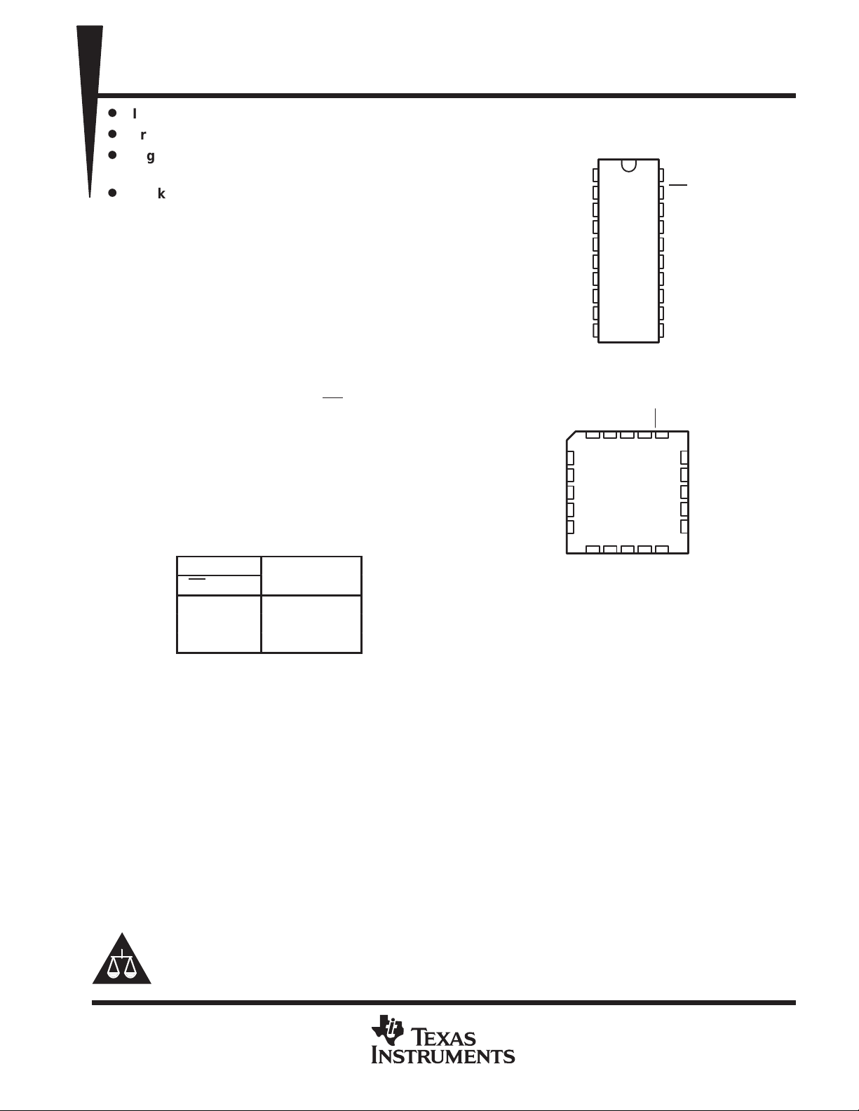
SN54HCT645 ...J OR W PACKAGE
SN74HCT645 . . . DW OR N PACKAGE
SN54HCT645 . . . FK PACKAGE
A3
A4
A5
A6
A7
(TOP VIEW)
1
DIR
2
A1
3
A2
4
A3
5
A4
6
A5
7
A6
8
A7
9
A8
10
GND
(TOP VIEW)
A2A1DIR
3212019
4
5
6
7
8
10 11 12 13
9
A8
B8
20
19
18
17
16
15
14
13
12
11
V
CC
B7
V
OE
B1
B2
B3
B4
B5
B6
B7
B8
OE
18
17
16
15
14
B6
CC
B1
B2
B3
B4
B5
GND
Please be aware that an important notice concerning availability, standard warranty, and use in critical applications of
Texas Instruments semiconductor products and disclaimers thereto appears at the end of this data sheet.
UNLESS OTHERWISE NOTED this document contains PRODUCTION
DATA information current as of publication date. Products conform to
specifications per the terms of Texas Instruments standard warranty.
Production processing does not necessarily include testing of all
parameters.
POST OFFICE BOX 655303 • DALLAS, TEXAS 75265
Copyright 1997, Texas Instruments Incorporated
1
SN54HCT645, SN74HCT645
OCTAL BUS TRANSCEIVERS
WITH 3-STATE OUTPUTS
SCLS019B – MARCH 1984 – REVISED MA Y 1997
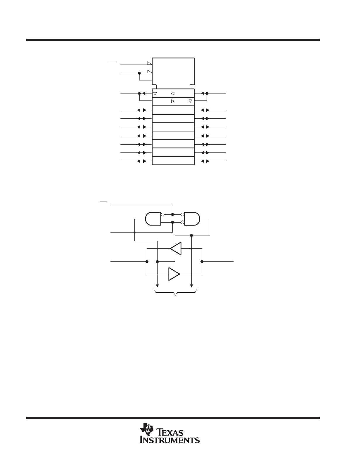
logic symbol
†
This symbol is in accordance with ANSI/IEEE Std 91-1984 and IEC Publication 617-12.
†
OE
DIR
A1
A2
A3
A4
A5
A6
A7
A8
19
1
2
3
4
5
6
7
8
9
G3
3 EN1 [BA]
3 EN2 [AB]
1
2
logic diagram (positive logic)
19
OE
18
17
16
15
14
13
12
11
B1
B2
B3
B4
B5
B6
B7
B8
1
DIR
218
A1
To Seven Other Transceivers
B1
2
POST OFFICE BOX 655303 • DALLAS, TEXAS 75265
 Loading...