

Texas Instruments SN74HCT623DW, SN74HCT623DWR, SN74HCT623N Datasheet
SN54HCT623, SN74HCT623
OCTAL BUS TRANSCEIVERS
WITH 3-STATE OUTPUTS
SCLS016B – MARCH 1984 – REVISED MA Y 1997
1
POST OFFICE BOX 655303 • DALLAS, TEXAS 75265
D
Inputs Are TTL-Voltage Compatible
D
Lock Bus-Latch Capability
D
True Logic
D
High-Current 3-State Outputs Can Drive up
to 15 LSTTL Loads
D
Package Options Include Plastic
Small-Outline (DW) and Ceramic Flat (W)
Packages, Ceramic Chip Carriers (FK), and
Standard Plastic (N) and Ceramic (J)
300-mil DIPs
description
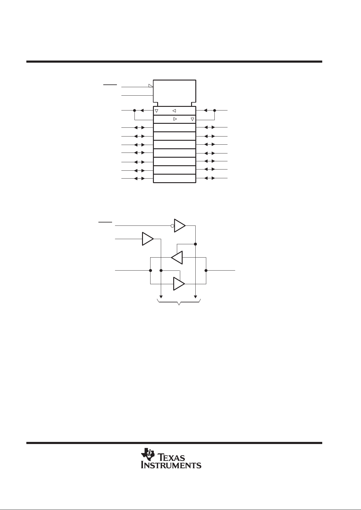
These octal bus transceivers are designed for
asynchronous two-way communication between
data buses. The control-function implementation
allows for maximum flexibility in timing.
The ’HCT623 allow data transmission from the
A bus to the B bus or from the B bus to the A bus,
depending upon the logic levels at the
output-enable (OEAB and OEBA
) inputs.
The output-enable inputs disable the device so
that the buses are effectively isolated. The
dual-enable configuration gives the transceivers
the capability to store data by simultaneously
enabling OEAB and OEBA
. Each output
reinforces its input in this transceiver
configuration. When both OEAB and OEBA are
enabled and all other data sources to the two sets
of bus lines are in the high-impedance state, both
sets of bus lines (16 total) remain at their last
states. The 8-bit codes appearing on the two sets
of buses are identical.
The SN54HCT623 is characterized for operation over the full military temperature range of –55°C to 125°C. The
SN74HCT623 is characterized for operation from –40°C to 85°C.
FUNCTION TABLE
INPUTS
OEBA OEAB
OPERATION
L L B data to A bus
H H A data to B bus
H L Isolation
L H
B data to A bus,
A data to B bus
Copyright 1997, Texas Instruments Incorporated
UNLESS OTHERWISE NOTED this document contains PRODUCTION
DATA information current as of publication date. Products conform to
specifications per the terms of Texas Instruments standard warranty.
Production processing does not necessarily include testing of all
parameters.
Please be aware that an important notice concerning availability, standard warranty, and use in critical applications of
Texas Instruments semiconductor products and disclaimers thereto appears at the end of this data sheet.
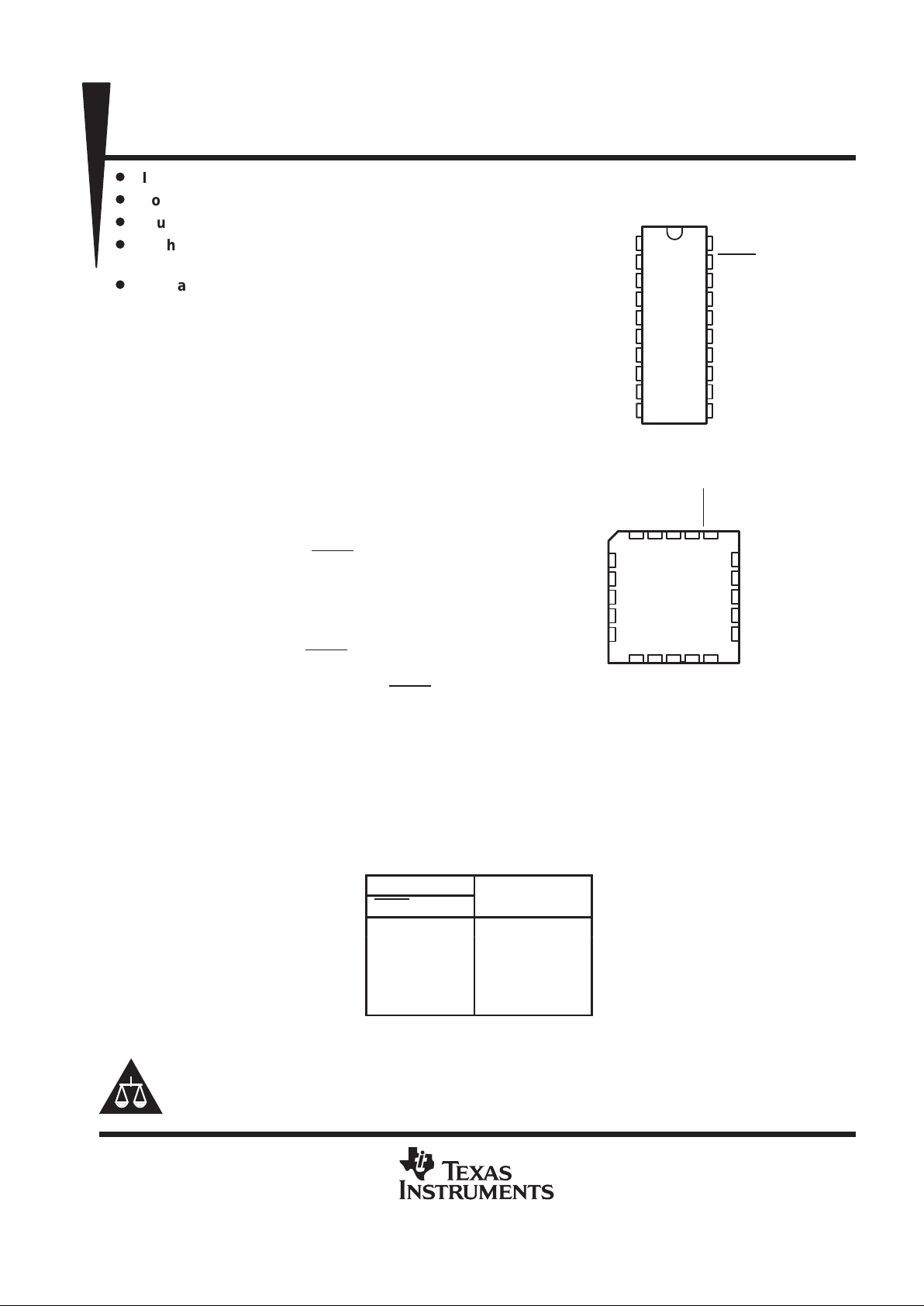
SN54HCT623 ...J OR W PACKAGE
SN74HCT623 . . . DW OR N PACKAGE
(TOP VIEW)
SN54HCT623 . . . FK PACKAGE
(TOP VIEW)
1
2
3
4
5
6
7
8
9
10
20
19
18
17
16
15
14
13
12
11
OEAB
A1
A2
A3
A4
A5
A6
A7
A8
GND
V
CC
OEBA
B1
B2
B3
B4
B5
B6
B7
B8
3212019
910111213
4
5
6
7
8
18
17
16
15
14
B1
B2
B3
B4
B5
A3
A4
A5
A6
A7
A2A1OEAB
B7
B6
V
OEBA
A8
GND
B8
CC
SN54HCT623, SN74HCT623
OCTAL BUS TRANSCEIVERS
WITH 3-STATE OUTPUTS
SCLS016B – MARCH 1984 – REVISED MA Y 1997
2
POST OFFICE BOX 655303 • DALLAS, TEXAS 75265
logic symbol
†
2
EN1
19
EN2
1
OEAB
2
A1
3
A2
B1
18
4
A3
5
A4
6
A5
7
A6
8
A7
9
A8
B2
17
B3
16
B5
14
B4
15
B6
13
B8
11
B7
12
OEBA
1
†
This symbol is in accordance with ANSI/IEEE Std 91-1984 and IEC Publication 617-12.
logic diagram (positive logic)
A1
B1
OEBA
OEAB
To Seven Other Transceivers
19
1
218
absolute maximum ratings over operating free-air temperature range
‡
Supply voltage range, VCC –0.5 V to 7 V. . . . . . . . . . . . . . . . . . . . . . . . . . . . . . . . . . . . . . . . . . . . . . . . . . . . . . . . . .
Input clamp current, I
IK
(VI < 0 or VI > VCC) (see Note 1) ±20 mA. . . . . . . . . . . . . . . . . . . . . . . . . . . . . . . . . . . .
Output clamp current, IOK (VO < 0 or VO > VCC) (see Note 1) ±20 mA. . . . . . . . . . . . . . . . . . . . . . . . . . . . . . . .
Continuous output current, IO (VO = 0 to VCC) ±35 mA. . . . . . . . . . . . . . . . . . . . . . . . . . . . . . . . . . . . . . . . . . . . . .
Continuous current through VCC or GND ±70 mA. . . . . . . . . . . . . . . . . . . . . . . . . . . . . . . . . . . . . . . . . . . . . . . . . . .
Package thermal impedance, θ
JA
(see Note 2): DW package 97°C/W. . . . . . . . . . . . . . . . . . . . . . . . . . . . . . . . .
N package 67°C/W. . . . . . . . . . . . . . . . . . . . . . . . . . . . . . . . . . .
Storage temperature range, T
stg
–65°C to 150°C. . . . . . . . . . . . . . . . . . . . . . . . . . . . . . . . . . . . . . . . . . . . . . . . . . .
‡
Stresses beyond those listed under “absolute maximum ratings” may cause permanent damage to the device. These are stress ratings only, and
functional operation of the device at these or any other conditions beyond those indicated under “recommended operating conditions” is not
implied. Exposure to absolute-maximum-rated conditions for extended periods may affect device reliability.
NOTES: 1. The input and output voltage ratings may be exceeded if the input and output current ratings are observed.
2. The package thermal impedance is calculated in accordance with JESD 51, except for through-hole packages, which use a trace
length of zero.
 Loading...