

Texas Instruments SN74HCT377DW, SN74HCT377DWR, SN74HCT377N Datasheet
SN54HCT377, SN74HCT377
OCTAL D-TYPE FLIP-FLOPS
WITH CLOCK ENABLE
SCLS067C – NOVEMBER 1988 – REVISED MA Y 1997
D
Inputs Are TTL-Voltage Compatible
D
Contain Eight Flip-Flops With Single-Rail
Outputs
D
Clock Enable Latched to Avoid False
Clocking
D
Applications Include:
– Buffer/Storage Registers
– Shift Registers
– Pattern Generators
D
Package Options Include Plastic
Small-Outline (DW), and Ceramic Flat (W)
Packages, Ceramic Chip Carriers (FK), and
Standard Plastic (N) and Ceramic (J)
300-mil DIPs
description
These devices are positive-edge-triggered D-type
flip-flops. The ’HCT377 are similar to the ’HCT273
but feature a latched clock-enable (CLKEN) input
instead of a common clear.
Information at the data (D) inputs meeting the
setup time requirements is transferred to the
Q outputs on the positive-going edge of the clock
(CLK) pulse if CLKEN
occurs at a particular voltage level and is not
directly related to the transition time of the
positive-going pulse. When CLK is at either the
high or low level, the D input has no effect at the
output. These devices are designed to prevent
false clocking by transitions at CLKEN
is low. Clock triggering
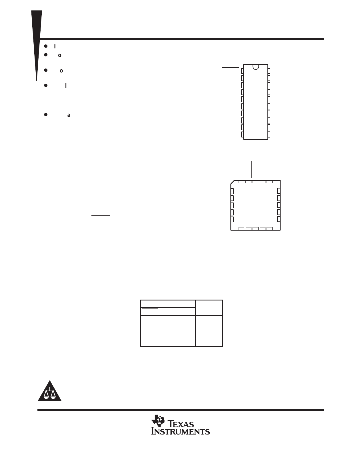
SN54HCT377 ...J OR W PACKAGE
SN74HCT377 . . . DW OR N PACKAGE
CLKEN
SN54HCT377 . . . FK PACKAGE
2D
2Q
3Q
3D
4D
(TOP VIEW)
1
1Q
2
1D
3
2D
4
2Q
5
3Q
6
3D
7
4D
8
4Q
9
GND
10
(TOP VIEW)
1D1QCLKEN
3212019
4
5
6
7
8
910111213
4Q
GND
20
19
18
17
16
15
14
13
12
11
CLK
CC
V
5Q
V
8Q
8D
7D
7Q
6Q
6D
5D
5Q
CLK
8Q
18
17
16
15
14
5D
CC
8D
7D
7Q
6Q
6D
.
The SN54HCT377 is characterized for operation over the full military temperature range of –55°C to 125°C. The
SN74HCT377 is characterized for operation from –40°C to 85°C.
FUNCTION TABLE
(each flip-flop)
Please be aware that an important notice concerning availability, standard warranty, and use in critical applications of
Texas Instruments semiconductor products and disclaimers thereto appears at the end of this data sheet.
UNLESS OTHERWISE NOTED this document contains PRODUCTION
DATA information current as of publication date. Products conform to
specifications per the terms of Texas Instruments standard warranty.
Production processing does not necessarily include testing of all
parameters.
INPUTS
CLKEN CLK D
H X X Q
L ↑ HH
L ↑ LL
X L X Q
OUTPUT
Q
0
0
Copyright 1997, Texas Instruments Incorporated
POST OFFICE BOX 655303 • DALLAS, TEXAS 75265
1
SN54HCT377, SN74HCT377
OCTAL D-TYPE FLIP-FLOPS
WITH CLOCK ENABLE
SCLS067C – NOVEMBER 1988 – REVISED MA Y 1997
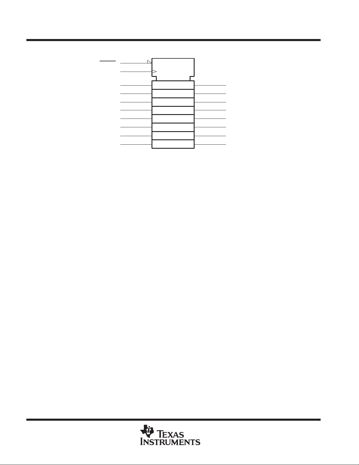
logic symbol
†
This symbol is in accordance with ANSI/IEEE Std 91-1984 and IEC Publication 617-12.
†
CLKEN
CLK
1D
2D
3D
4D
5D
6D
7D
8D
1
11
3
4
7
8
13
14
17
18
G1
1C2
2D
12
15
16
19
2
1Q
5
2Q
6
3Q
9
4Q
5Q
6Q
7Q
8Q
2
POST OFFICE BOX 655303 • DALLAS, TEXAS 75265
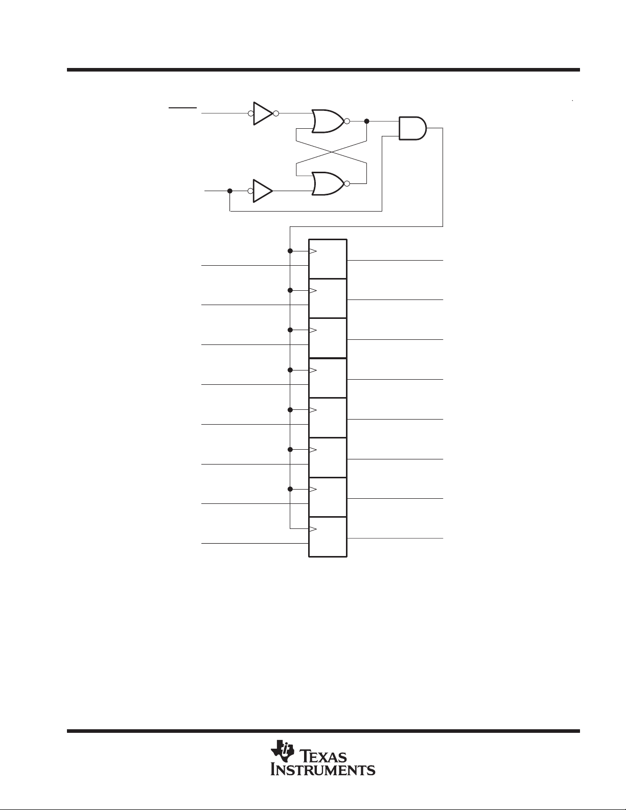
logic diagram (positive logic)
SN54HCT377, SN74HCT377
OCTAL D-TYPE FLIP-FLOPS
WITH CLOCK ENABLE
SCLS067C – NOVEMBER 1988 – REVISED MA Y 1997
CLKEN
CLK
1D
2D
3D
4D
1
11
3
4
7
8
C1
1D
C1
1D
C1
1D
C1
1D
2
1Q
5
2Q
6
3Q
9
4Q
5D
6D
7D
8D
13
14
17
18
1D
1D
1D
1D
C1
C1
C1
C1
12
15
16
19
5Q
6Q
7Q
8Q
POST OFFICE BOX 655303 • DALLAS, TEXAS 75265
3
 Loading...