

SN54HCT377, SN74HCT377
OCTAL D-TYPE FLIP-FLOPS
WITH CLOCK ENABLE
SCLS067C – NOVEMBER 1988 – REVISED MA Y 1997
D
Inputs Are TTL-Voltage Compatible
D
Contain Eight Flip-Flops With Single-Rail
Outputs
D
Clock Enable Latched to Avoid False
Clocking
D
Applications Include:
– Buffer/Storage Registers
– Shift Registers
– Pattern Generators
D
Package Options Include Plastic
Small-Outline (DW), and Ceramic Flat (W)
Packages, Ceramic Chip Carriers (FK), and
Standard Plastic (N) and Ceramic (J)
300-mil DIPs
description
These devices are positive-edge-triggered D-type
flip-flops. The ’HCT377 are similar to the ’HCT273
but feature a latched clock-enable (CLKEN) input
instead of a common clear.
Information at the data (D) inputs meeting the
setup time requirements is transferred to the
Q outputs on the positive-going edge of the clock
(CLK) pulse if CLKEN
occurs at a particular voltage level and is not
directly related to the transition time of the
positive-going pulse. When CLK is at either the
high or low level, the D input has no effect at the
output. These devices are designed to prevent
false clocking by transitions at CLKEN
is low. Clock triggering
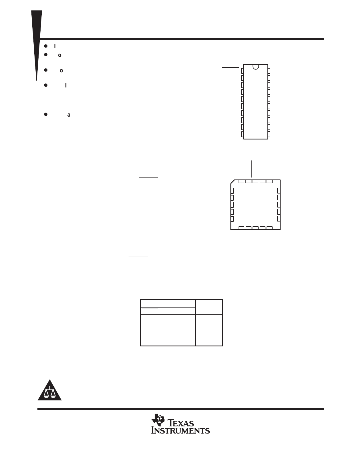
SN54HCT377 ...J OR W PACKAGE
SN74HCT377 . . . DW OR N PACKAGE
CLKEN
SN54HCT377 . . . FK PACKAGE
2D
2Q
3Q
3D
4D
(TOP VIEW)
1
1Q
2
1D
3
2D
4
2Q
5
3Q
6
3D
7
4D
8
4Q
9
GND
10
(TOP VIEW)
1D1QCLKEN
3212019
4
5
6
7
8
910111213
4Q
GND
20
19
18
17
16
15
14
13
12
11
CLK
CC
V
5Q
V
8Q
8D
7D
7Q
6Q
6D
5D
5Q
CLK
8Q
18
17
16
15
14
5D
CC
8D
7D
7Q
6Q
6D
.
The SN54HCT377 is characterized for operation over the full military temperature range of –55°C to 125°C. The
SN74HCT377 is characterized for operation from –40°C to 85°C.
FUNCTION TABLE
(each flip-flop)
Please be aware that an important notice concerning availability, standard warranty, and use in critical applications of
Texas Instruments semiconductor products and disclaimers thereto appears at the end of this data sheet.
UNLESS OTHERWISE NOTED this document contains PRODUCTION
DATA information current as of publication date. Products conform to
specifications per the terms of Texas Instruments standard warranty.
Production processing does not necessarily include testing of all
parameters.
INPUTS
CLKEN CLK D
H X X Q
L ↑ HH
L ↑ LL
X L X Q
OUTPUT
Q
0
0
Copyright 1997, Texas Instruments Incorporated
POST OFFICE BOX 655303 • DALLAS, TEXAS 75265
1
SN54HCT377, SN74HCT377
OCTAL D-TYPE FLIP-FLOPS
WITH CLOCK ENABLE
SCLS067C – NOVEMBER 1988 – REVISED MA Y 1997
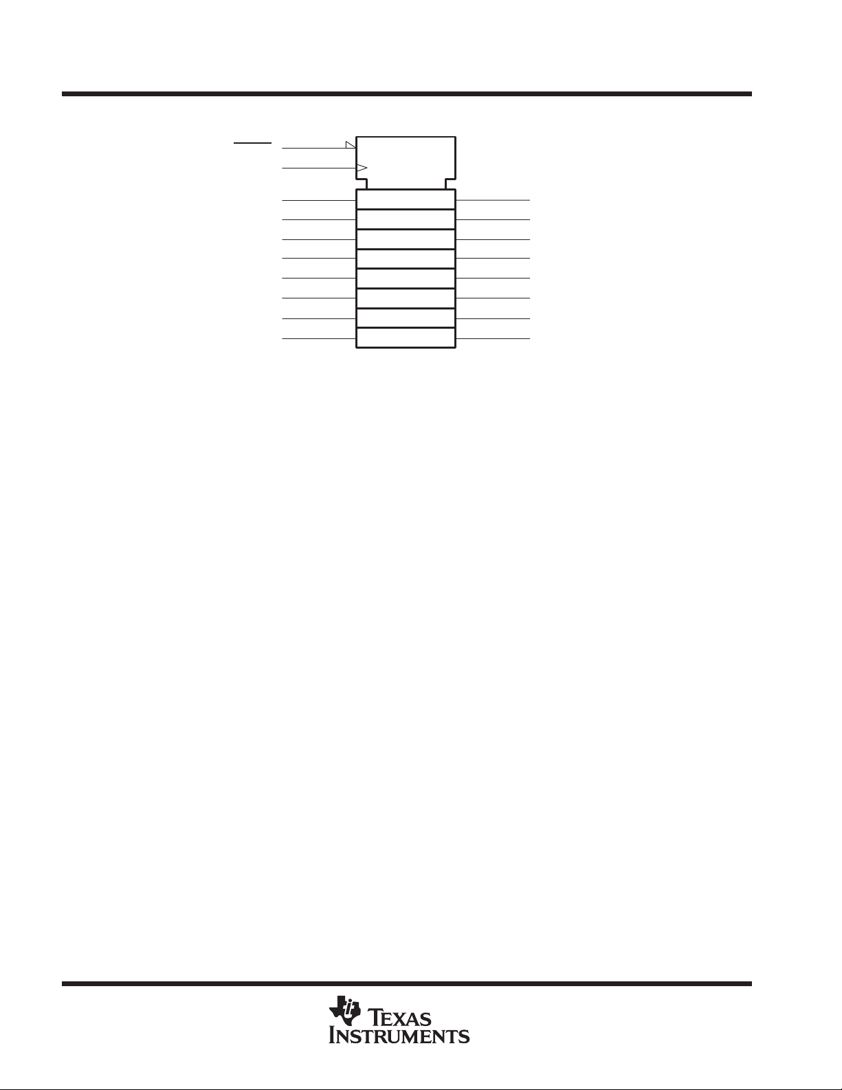
logic symbol
†
This symbol is in accordance with ANSI/IEEE Std 91-1984 and IEC Publication 617-12.
†
CLKEN
CLK
1D
2D
3D
4D
5D
6D
7D
8D
1
11
3
4
7
8
13
14
17
18
G1
1C2
2D
12
15
16
19
2
1Q
5
2Q
6
3Q
9
4Q
5Q
6Q
7Q
8Q
2
POST OFFICE BOX 655303 • DALLAS, TEXAS 75265
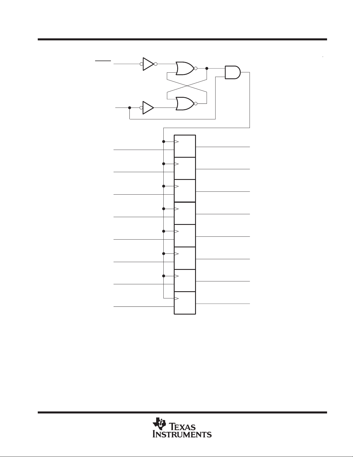
logic diagram (positive logic)
SN54HCT377, SN74HCT377
OCTAL D-TYPE FLIP-FLOPS
WITH CLOCK ENABLE
SCLS067C – NOVEMBER 1988 – REVISED MA Y 1997
CLKEN
CLK
1D
2D
3D
4D
1
11
3
4
7
8
C1
1D
C1
1D
C1
1D
C1
1D
2
1Q
5
2Q
6
3Q
9
4Q
5D
6D
7D
8D
13
14
17
18
1D
1D
1D
1D
C1
C1
C1
C1
12
15
16
19
5Q
6Q
7Q
8Q
POST OFFICE BOX 655303 • DALLAS, TEXAS 75265
3

SN54HCT377, SN74HCT377
UNIT
PARAMETER
TEST CONDITIONS
V
UNIT
V
V
V
V
V
V
V
V
V
V
OCTAL D-TYPE FLIP-FLOPS
WITH CLOCK ENABLE
SCLS067C – NOVEMBER 1988 – REVISED MA Y 1997
absolute maximum ratings over operating free-air temperature range
Supply voltage range, V
–0.5 V to 7 V. . . . . . . . . . . . . . . . . . . . . . . . . . . . . . . . . . . . . . . . . . . . . . . . . . . . . . . . . .
CC
†
Input clamp current, IIK (VI < 0 or VI > VCC) (see Note 1) ±20 mA. . . . . . . . . . . . . . . . . . . . . . . . . . . . . . . . . . . .
Output clamp current, IOK (VO < 0 or VO > VCC) (see Note 1) ±20 mA. . . . . . . . . . . . . . . . . . . . . . . . . . . . . . . .
Continuous output current, IO (VO = 0 to VCC) ±25 mA. . . . . . . . . . . . . . . . . . . . . . . . . . . . . . . . . . . . . . . . . . . . . .
Continuous current through VCC or GND ±50 mA. . . . . . . . . . . . . . . . . . . . . . . . . . . . . . . . . . . . . . . . . . . . . . . . . . .
Package thermal impedance, θ
(see Note 2): DW package 97°C/W. . . . . . . . . . . . . . . . . . . . . . . . . . . . . . . . .
JA
N package 67°C/W. . . . . . . . . . . . . . . . . . . . . . . . . . . . . . . . . . .
Storage temperature range, T
†
Stresses beyond those listed under “absolute maximum ratings” may cause permanent damage to the device. These are stress ratings only, and
functional operation of the device at these or any other conditions beyond those indicated under “recommended operating conditions” is not
implied. Exposure to absolute-maximum-rated conditions for extended periods may affect device reliability.
NOTES: 1. The input and output voltage ratings may be exceeded if the input and output current ratings are observed.
2. The package thermal impedance is calculated in accordance with JESD 51, except for through-hole packages, which use a trace
length of zero.
–65°C to 150°C. . . . . . . . . . . . . . . . . . . . . . . . . . . . . . . . . . . . . . . . . . . . . . . . . . .
stg
recommended operating conditions
SN54HCT377 SN74HCT377
MIN NOM MAX MIN NOM MAX
V
V
V
V
V
t
t
T
Supply voltage 4.5 5 5.5 4.5 5 5.5 V
CC
High-level input voltage VCC = 4.5 V to 5.5 V 2 2 V
IH
Low-level input voltage VCC = 4.5 V to 5.5 V 0 0.8 0 0.8 V
IL
Input voltage 0 V
I
Output voltage 0 V
O
Input transition (rise and fall) times 0 500 0 500 ns
Operating free-air temperature –55 125 –40 85 °C
A
CC
CC
0 V
0 V
CC
CC
V
V
electrical characteristics over recommended operating free-air temperature range (unless
otherwise noted)
CC
=
OH
OL
I
I
I
CC
‡
∆I
CC
C
i
* On products compliant to MIL-PRF-38535, this parameter is not production tested.
‡
This is the increase in supply current for each input that is at one of the specified TTL voltage levels rather than 0 V or VCC.
or
I
IH
=
or
I
IH
VI = VCC or 0 5.5 V ±0.1 ±100 ±1000 ±1000 nA
VI = VCC or 0, IO = 0 5.5 V 8 160 80 µA
One input at 0.5 V or 2.4 V,
Other inputs at GND or V
IOH = –20 µA 4.5 V 4.4 4.499 4.4 4.4
IL
IOH = –4 mA 4.5 V 3.98 4.30 3.7 3.84
IOL = 20 µA 4.5 V 0.001 0.1 0.1 0.1
IL
IOL = 4 mA 4.5 V 0.17 0.26 0.4 0.33
CC
5.5 V 1.4 2.4 3 2.9 mA
4.5 V to
5.5 V
TA = 25°C SN54HCT377 SN74HCT377
MIN TYP MAX MIN MAX MIN MAX
3 10 10* 10 pF
PRODUCT PREVIEW information concerns products in the formative or
design phase of development. Characteristic data and other
specifications are design goals. Texas Instruments reserves the right to
change or discontinue these products without notice.
4
POST OFFICE BOX 655303 • DALLAS, TEXAS 75265

V
UNIT
f
Clock frequenc
MH
twPulse duration
CLK high or lo
ns
Data
tsuSetup time before CLK↑
ns
CLKEN high
Data
thHold time data after CLK↑
ns
CLKEN inactive or active
(INPUT)
(OUTPUT)
MIN
MAX
f
MH
t
CLK
An
ns
ttAn
ns
(INPUT)
(OUTPUT)
MIN
MAX
f
MH
t
CLK
An
ns
ttAn
ns
SN54HCT377, SN74HCT377
OCTAL D-TYPE FLIP-FLOPS
WITH CLOCK ENABLE
SCLS067C – NOVEMBER 1988 – REVISED MA Y 1997
timing requirements over recommended operating free-air temperature range (unless otherwise
noted)
TA = 25°C SN54HCT377 SN74HCT377
CC
MIN MAX MIN MAX MIN MAX
clock
p
y
w
or low
switching characteristics over recommended operating free-air temperature range, CL = 50 pF (unless
otherwise noted) (see Figure 1)
PARAMETER
max
pd
FROM
4.5 V 0 25 0 17 0 20
5.5 V
4.5 V 20 30 25
5.5 V 18 28 23
4.5 V 12 18 15
5.5 V 10 17 14
4.5 V 12 18 15
5.5 V 10 17 14
4.5 V 3 3 3
5.5 V 3 3 3
4.5 V 5 5 5
5.5 V 5 5 5
TO
y
y
0 30 0 19 0 22
SN54HCT377
V
CC
4.5 V 25 31 17
5.5 V 30 37 19
4.5 V 15 30 45
5.5 V 12 28 40
4.5 V 8 15 22
5.5 V 6 14 21
TA = 25°C
MIN TYP MAX
z
UNIT
z
switching characteristics over recommended operating free-air temperature range, CL = 50 pF (unless
otherwise noted) (see Figure 1)
operating characteristics, TA = 25°C
C
pd
PRODUCT PREVIEW information concerns products in the formative or
design phase of development. Characteristic data and other
specifications are design goals. Texas Instruments reserves the right to
change or discontinue these products without notice.
PARAMETER
max
pd
Power dissipation capacitance No load 30 pF
FROM
PARAMETER TEST CONDITIONS TYP UNIT
POST OFFICE BOX 655303 • DALLAS, TEXAS 75265
TO
V
CC
MIN TYP MAX
4.5 V 25 31 20
5.5 V 30 37 22
y
y
4.5 V 15 30 38
5.5 V 12 28 35
4.5 V 8 15 19
5.5 V 6 14 17
SN74HCT377
TA = 25°C
UNIT
z
5

SN54HCT377, SN74HCT377
S
OCTAL D-TYPE FLIP-FLOPS
WITH CLOCK ENABLE
SCLS067C – NOVEMBER 1988 – REVISED MA Y 1997
PARAMETER MEASUREMENT INFORMATION
From Output
Under Test
LOAD CIRCUIT
Input
In-Phase
Output
Out-of-
Phase
Output
PROPAGATION DELAY AND OUTPUT RISE AND FALL TIMES
NOTES: A. CL includes probe and test-fixture capacitance.
B. Phase relationships between waveforms were chosen arbitrarily. All input pulses are supplied by generators having the following
C. The outputs are measured one at a time with one input transition per measurement.
D. For clock inputs, f
E. t
1.3 V
t
PLH
t
PHL
VOLTAGE WAVEFORMS
characteristics: PRR ≤ 1 MHz, ZO = 50 Ω, tr = 6 ns, tf = 6 ns.
PLH
and t
max
are the same as tpd.
PHL
Test
Point
CL = 50 pF
(see Note A)
1.3 V
t
PHL
90% 90%
t
r
t
PLH
1.3 V 1.3 V
10% 10%
t
f
is measured when the input duty cycle is 50%.
High-Level
Pulse
Low-Level
Pulse
3 V
0 V
V
OH
f
r
V
OL
V
OH
V
OL
Reference
Input
Data
Input
SETUP AND HOLD AND INPUT RISE AND FALL TIME
1.3 V1.3 V
10%10%
t
90%90%
t
1.3 V
t
w
1.3 V
VOLTAGE WAVEFORMS
PULSE DURATIONS
1.3 V
t
su
2.7 V 2.7 V
t
r
VOLTAGE WAVEFORMS
1.3 V
1.3 V
t
h
3 V
0 V
3 V
0 V
3 V
0 V
3 V
1.3 V1.3 V
0.3 V0.3 V
0 V
t
f
Figure 1. Load Circuit and Voltage Waveforms
6
POST OFFICE BOX 655303 • DALLAS, TEXAS 75265

IMPORTANT NOTICE
T exas Instruments and its subsidiaries (TI) reserve the right to make changes to their products or to discontinue
any product or service without notice, and advise customers to obtain the latest version of relevant information
to verify, before placing orders, that information being relied on is current and complete. All products are sold
subject to the terms and conditions of sale supplied at the time of order acknowledgement, including those
pertaining to warranty, patent infringement, and limitation of liability.
TI warrants performance of its semiconductor products to the specifications applicable at the time of sale in
accordance with TI’s standard warranty. Testing and other quality control techniques are utilized to the extent
TI deems necessary to support this warranty . Specific testing of all parameters of each device is not necessarily
performed, except those mandated by government requirements.
CERTAIN APPLICA TIONS USING SEMICONDUCT OR PRODUCTS MAY INVOLVE POTENTIAL RISKS OF
DEATH, PERSONAL INJURY, OR SEVERE PROPERTY OR ENVIRONMENTAL DAMAGE (“CRITICAL
APPLICATIONS”). TI SEMICONDUCTOR PRODUCTS ARE NOT DESIGNED, AUTHORIZED, OR
WARRANTED TO BE SUITABLE FOR USE IN LIFE-SUPPORT DEVICES OR SYSTEMS OR OTHER
CRITICAL APPLICA TIONS. INCLUSION OF TI PRODUCTS IN SUCH APPLICATIONS IS UNDERST OOD TO
BE FULLY AT THE CUSTOMER’S RISK.
In order to minimize risks associated with the customer’s applications, adequate design and operating
safeguards must be provided by the customer to minimize inherent or procedural hazards.
TI assumes no liability for applications assistance or customer product design. TI does not warrant or represent
that any license, either express or implied, is granted under any patent right, copyright, mask work right, or other
intellectual property right of TI covering or relating to any combination, machine, or process in which such
semiconductor products or services might be or are used. TI’s publication of information regarding any third
party’s products or services does not constitute TI’s approval, warranty or endorsement thereof.
Copyright 1998, Texas Instruments Incorporated
 Loading...