

Texas Instruments SN74HCT125D, SN74HCT125DR, SN74HCT125N Datasheet
SN54HCT125, SN74HCT125
QUADRUPLE BUS BUFFER GATES
WITH 3-STATE OUTPUTS
SCLS069C – NOVEMBER 1988 – REVISED MA Y 1997
1
POST OFFICE BOX 655303 • DALLAS, TEXAS 75265
D
Inputs Are TTL-Voltage Compatible
D
High-Current 3-State Outputs Drive Bus
Lines or Buffer Memory Address Registers
D
Package Options Include Plastic
Small-Outline (D) and Ceramic Flat (W)
Packages, Ceramic Chip Carriers (FK), and
Standard Plastic (N) and Ceramic (J)
300-mil DIPs
description
These bus buffer gates feature independent line
drivers with 3-state outputs. Each output is
disasbled when the associated output-enable
(OE
) input is high.
The SN54HCT125 is characterized for operation
over the full military temperature range of –55°C
to 125°C. The SN74HCT125 is characterized for
operation from –40°C to 85°C.
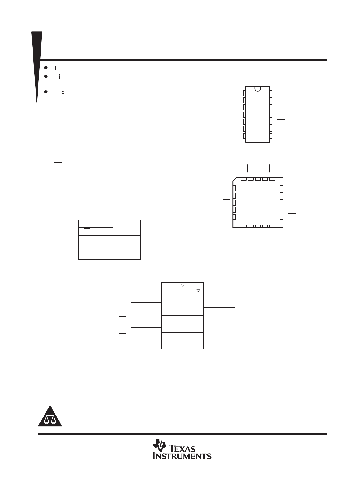
FUNCTION TABLE
(each gate)
INPUTS
OUTPUT
OE A
Y
L H H
L LL
H X Z
logic symbol
†
EN
1
2
1B
4
5
2B
10
9
3B
13
12
4B
†
This symbol is in accordance with ANSI/IEEE Std 91-1984 and IEC Publication 617-12.
Pin numbers shown are for the D, J, N, and W packages.
1Y
3
1OE
2OE
3OE
4OE
2Y
6
3Y
8
4Y
11
Copyright 1997, Texas Instruments Incorporated
UNLESS OTHERWISE NOTED this document contains PRODUCTION
DATA information current as of publication date. Products conform to
specifications per the terms of Texas Instruments standard warranty.
Production processing does not necessarily include testing of all
parameters.
Please be aware that an important notice concerning availability, standard warranty, and use in critical applications of
Texas Instruments semiconductor products and disclaimers thereto appears at the end of this data sheet.
SN54HCT125 ...J OR W PACKAGE
SN74HCT125 ...D OR N PACKAGE
(TOP VIEW)
3212019
910111213
4
5
6
7
8
18
17
16
15
14
4A
NC
4Y
NC
3OE
1Y
NC
2OE
NC
2A
1A
1OE
NC
3Y
3A
V
4OE
2Y
GND
NC
SN54HCT125 . . . FK PACKAGE
(TOP VIEW)
CC
NC – No internal connection
1
2
3
4
5
6
7
14
13
12
11
10
9
8
1OE
1A
1Y
2OE
2A
2Y
GND
V
CC
4OE
4A
4Y
3OE
3A
3Y
SN54HCT125, SN74HCT125
QUADRUPLE BUS BUFFER GATES
WITH 3-STATE OUTPUTS
SCLS069C – NOVEMBER 1988 – REVISED MA Y 1997
2
POST OFFICE BOX 655303 • DALLAS, TEXAS 75265
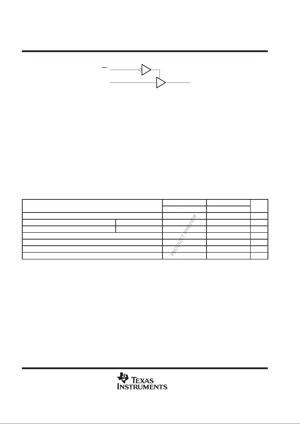
logic diagram (positive logic)
AY
OE
absolute maximum ratings over operating free-air temperature range
†
Supply voltage range, VCC –0.5 V to 7 V. . . . . . . . . . . . . . . . . . . . . . . . . . . . . . . . . . . . . . . . . . . . . . . . . . . . . . . . . .
Input clamp current, IIK (VI < 0 or VI > VCC) (see Note 1) ±20 mA. . . . . . . . . . . . . . . . . . . . . . . . . . . . . . . . . . . .
Output clamp current, I
OK
(VO < 0 or VO > VCC) (see Note 1) ±20 mA. . . . . . . . . . . . . . . . . . . . . . . . . . . . . . . .
Continuous output current, IO (VO = 0 to VCC) ±35 mA. . . . . . . . . . . . . . . . . . . . . . . . . . . . . . . . . . . . . . . . . . . . . .
Continuous current through VCC or GND ±70 mA. . . . . . . . . . . . . . . . . . . . . . . . . . . . . . . . . . . . . . . . . . . . . . . . . . .
Package thermal impedance, θ
JA
(see Note 2): D package 127°C/W. . . . . . . . . . . . . . . . . . . . . . . . . . . . . . . . . .
N package 78°C/W. . . . . . . . . . . . . . . . . . . . . . . . . . . . . . . . . . .
Storage temperature range, T
stg
–65°C to 150°C. . . . . . . . . . . . . . . . . . . . . . . . . . . . . . . . . . . . . . . . . . . . . . . . . . .
†
Stresses beyond those listed under “absolute maximum ratings” may cause permanent damage to the device. These are stress ratings only, and
functional operation of the device at these or any other conditions beyond those indicated under “recommended operating conditions” is not
implied. Exposure to absolute-maximum-rated conditions for extended periods may affect device reliability.
NOTES: 1. The input and output voltage ratings may be exceeded if the input and output current ratings are observed.
2. The package thermal impedance is calculated in accordance with JESD 51, except for through-hole packages, which use a trace
length of zero.
recommended operating conditions
SN54HCT125 SN74HCT125
MIN NOM MAX MIN NOM MAX
UNIT
V
CC
Supply voltage 4.5 5 5.5 4.5 5 5.5 V
V
IH
High-level input voltage VCC = 4.5 V to 5.5 V 2 2 V
V
IL
Low-level input voltage VCC = 4.5 V to 5.5 V 0 0.8 0 0.8 V
V
I
Input voltage 0 V
CC
0 V
CC
V
V
O
Output voltage 0 V
CC
0 V
CC
V
t
t
Input transition (rise and fall) time 0 500 0 500 ns
T
A
Operating free-air temperature –55 125 –40 85 °C
PRODUCT PREVIEW information concerns products in the formative or
design phase of development. Characteristic data and other
specifications are design goals. Texas Instruments reserves the right to
change or discontinue these products without notice.
 Loading...