

Texas Instruments SN74HC7001D, SN74HC7001DR, SN74HC7001N, SN74HC7001N3 Datasheet
SN54HC7001, SN74HC7001
QUADRUPLE POSITIVE-AND GATES
WITH SCHMITT-TRIGGER INPUTS
SCLS035B – MARCH 1984 – REVISED MA Y 1997
D
Operation From Very Slow Input
Transitions
D
T emperature-Compensated Threshold
Levels
D
High Noise Immunity
D
Same Pinouts as ’HC08
D
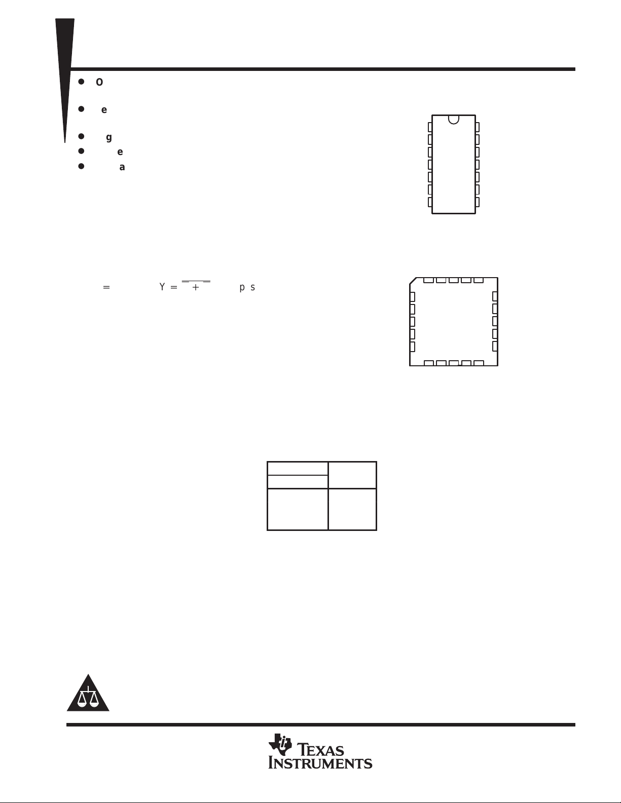
Package Options Include Plastic
Small-Outline (D) and Ceramic Flat (W)
Packages, Ceramic Chip Carriers (FK), and
Standard Plastic (N) and Ceramic (J)
300-mil DIPs
description
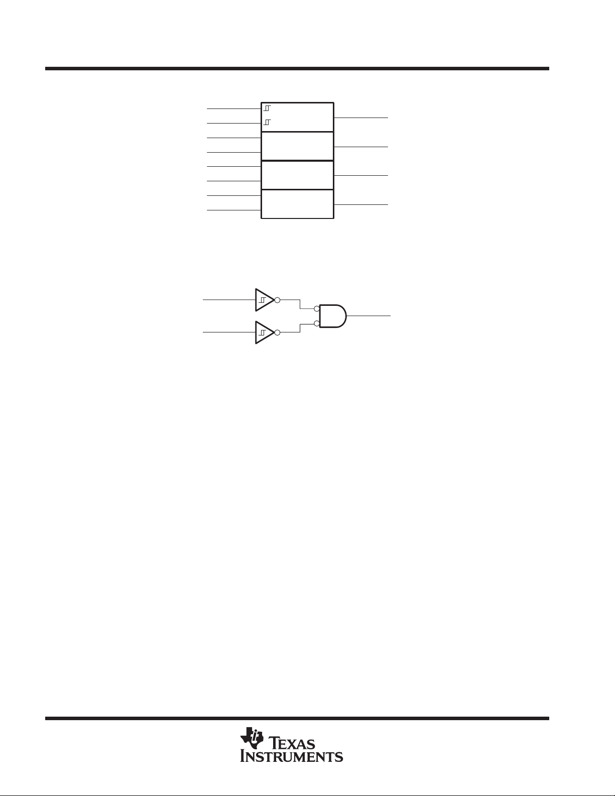
Each circuit functions as a quadruple AND gate.
They perform the Boolean function
Y+A • BorY+A)B
Because of the Schmitt action, the inputs have
different input threshold levels for positive- and
negative-going signals.
These circuits are temperature compensated and
can be triggered from the slowest of input ramps
and still give clean jitter-free output signals.
The SN54HC7001 is characterized for operation
over the full military temperature range of –55°C
to 125°C. The SN74HC7001 is characterized for
operation from –40°C to 85°C.
in positive logic.
SN54HC7001 . . . J OR W PACKAGE
SN74HC7001 ...D OR N PACKAGE
SN54HC7001 . . . FK PACKAGE
1Y
NC
2A
NC
2B
NC – No internal connection
(TOP VIEW)
1A
1
1B
2
1Y
3
2A
4
2B
5
6
2Y
GND
7
(TOP VIEW)
1B1ANC
3212019
4
5
6
7
8
910111213
2Y
GND
NC
14
13
12
11
10
9
8
CC
V
3Y
V
4B
4A
4Y
3B
3A
3Y
4B
18
17
16
15
14
3A
CC
4A
NC
4Y
NC
3B
Please be aware that an important notice concerning availability, standard warranty, and use in critical applications of
Texas Instruments semiconductor products and disclaimers thereto appears at the end of this data sheet.
UNLESS OTHERWISE NOTED this document contains PRODUCTION
DATA information current as of publication date. Products conform to
specifications per the terms of Texas Instruments standard warranty.
Production processing does not necessarily include testing of all
parameters.
FUNCTION TABLE
(each gate)
INPUTS
A B
H H H
L XL
X L L
OUTPUT
Y
Copyright 1997, Texas Instruments Incorporated
POST OFFICE BOX 655303 • DALLAS, TEXAS 75265
1
SN54HC7001, SN74HC7001
QUADRUPLE POSITIVE-AND GATES
WITH SCHMITT-TRIGGER INPUTS
SCLS035B – MARCH 1984 – REVISED MA Y 1997
logic symbol
†
This symbol is in accordance with ANSI/IEEE Std 91-1984 and IEC Publication 617-12.
Pin numbers shown are for the D, J, N, and W packages.
†
1
1A
1B
2A
2B
3A
3B
4A
4B
2
4
5
9
10
12
13
&
3
1Y
6
2Y
8
3Y
11
4Y
logic diagram, each gate (positive logic)
A
Y
B
absolute maximum ratings over operating free-air temperature range
‡
Supply voltage range, VCC –0.5 V to 7 V. . . . . . . . . . . . . . . . . . . . . . . . . . . . . . . . . . . . . . . . . . . . . . . . . . . . . . . . . .
Input clamp current, IIK (VI < 0 or VI > VCC) (see Note 1) ±20 mA. . . . . . . . . . . . . . . . . . . . . . . . . . . . . . . . . . . .
Output clamp current, IOK (VO < 0 or VO > VCC) (see Note 1) ±20 mA. . . . . . . . . . . . . . . . . . . . . . . . . . . . . . . .
Continuous output current, I
(VO = 0 to VCC) ±25 mA. . . . . . . . . . . . . . . . . . . . . . . . . . . . . . . . . . . . . . . . . . . . . .
O
Continuous current through VCC or GND ±50 mA. . . . . . . . . . . . . . . . . . . . . . . . . . . . . . . . . . . . . . . . . . . . . . . . . . .
Package thermal impedance, θ
(see Note 2): D package 127°C/W. . . . . . . . . . . . . . . . . . . . . . . . . . . . . . . . . .
JA
N package 78°C/W. . . . . . . . . . . . . . . . . . . . . . . . . . . . . . . . . . .
Storage temperature range, T
‡
Stresses beyond those listed under “absolute maximum ratings” may cause permanent damage to the device. These are stress ratings only, and
functional operation of the device at these or any other conditions beyond those indicated under “recommended operating conditions” is not
implied. Exposure to absolute-maximum-rated conditions for extended periods may affect device reliability.
NOTES: 1. The input and output voltage ratings may be exceeded if the input and output current ratings are observed.
2. The package thermal impedance is calculated in accordance with JESD 51, except for through-hole packages, which use a trace
length of zero.
–65°C to 150°C. . . . . . . . . . . . . . . . . . . . . . . . . . . . . . . . . . . . . . . . . . . . . . . . . . .
stg
2
POST OFFICE BOX 655303 • DALLAS, TEXAS 75265
 Loading...