

Texas Instruments SN74HC594DW, SN74HC594DWR, SN74HC594N Datasheet
SN54HC594, SN74HC594
8-BIT SHIFT REGISTERS
WITH OUTPUT REGISTERS
SCLS040C – DECEMBER 1982 – REVISED FEBRUARY 1998
1
POST OFFICE BOX 655303 • DALLAS, TEXAS 75265
D
8-Bit Serial-In, Parallel-Out Shift Registers
With Storage
D
Independent Direct Overriding Clears on
Shift and Storage Registers
D
Independent Clocks for Both Shift and
Storage Registers
D
High-Current Outputs Can Drive Up to
15 LSTTL Loads
D
Package Options Include Plastic
Small-Outline (D), Shrink Small-Outline
(DB), and Ceramic Flat (W) Packages,
Ceramic Chip Carriers (FK), and Standard
Plastic (N) and Ceramic (J) 300-mil DIPs
description
The ’HC594 devices contain an 8-bit serial-in,
parallel-out shift register that feeds an 8-bit D-type
storage register. Separate clocks and direct
overriding clear (RCLR
, SRCLR) inputs are
provided on both the shift and storage registers.
A serial (Q
H′
) output is provided for cascading
purposes.
Both the shift register (RCLK) and storage register
(SRCLK) clocks are positive edge triggered. If
both clocks are connected together, the shift
register is always one count pulse ahead of the
storage register.
The parallel (Q
A–QH
) outputs have high-current
capability. Q
H′
is a standard output.
The SN54HC594 is characterized for operation over the full military temperature range of –55°C to 125°C. The
SN74HC594 is characterized for operation from –40°C to 85°C.
Copyright 1998, Texas Instruments Incorporated
UNLESS OTHERWISE NOTED this document contains PRODUCTION
DATA information current as of publication date. Products conform to
specifications per the terms of Texas Instruments standard warranty.
Production processing does not necessarily include testing of all
parameters.
Please be aware that an important notice concerning availability, standard warranty, and use in critical applications of
Texas Instruments semiconductor products and disclaimers thereto appears at the end of this data sheet.
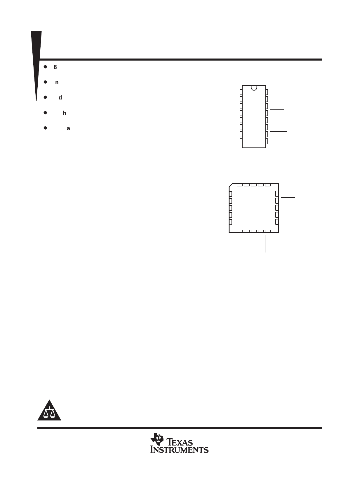
SN54HC594 ...J OR W PACKAGE
SN74HC594 . . . D, DB, OR N PACKAGE
(TOP VIEW)
SN54HC594 . . . FK PACKAGE
(TOP VIEW)
NC – No internal connection
1
2
3
4
5
6
7
8
16
15
14
13
12
11
10
9
Q
B
Q
C
Q
D
Q
E
Q
F
Q
G
Q
H
GND
V
CC
Q
A
SER
RCLR
RCLK
SRCLK
SRCLR
Q
H′
3212019
910111213
4
5
6
7
8
18
17
16
15
14
SER
RCLR
NC
RCLK
SRCLK
Q
D
Q
E
NC
Q
F
Q
G
Q
NC
SRCLR
H
GND
NC
CQB
VCCQ
A
Q
H
Q
′
SN54HC594, SN74HC594
8-BIT SHIFT REGISTERS
WITH OUTPUT REGISTERS
SCLS040C – DECEMBER 1982 – REVISED FEBRUARY 1998
2
POST OFFICE BOX 655303 • DALLAS, TEXAS 75265
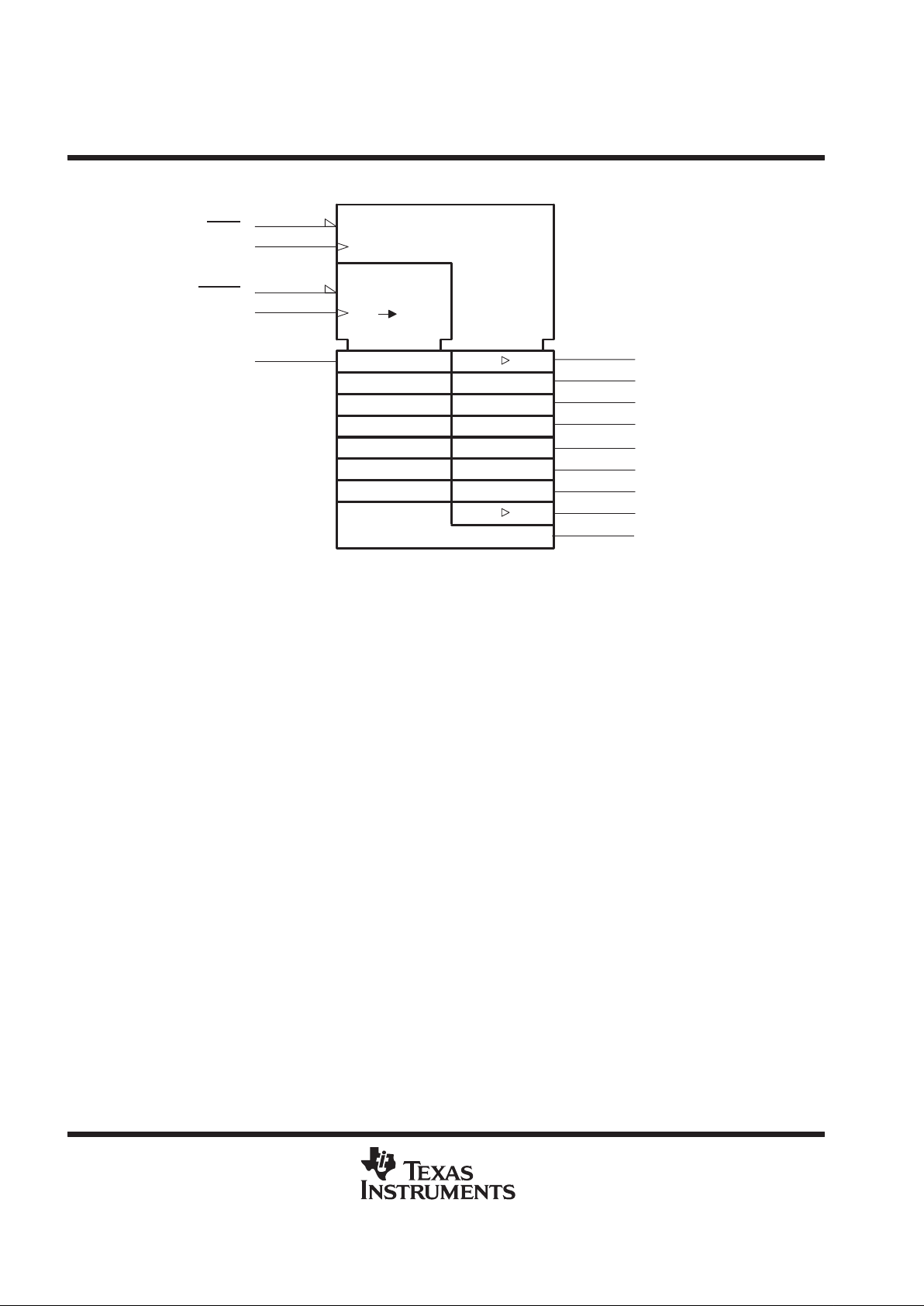
logic symbol
†
R
10
15
3
1
2
3
11
SRCLK
R3
13
12
RCLK
C2
4
5
6
7
3
2D
†
This symbol is in accordance with ANSI/IEEE Std 91-1984 and IEC Publication 617-12.
Pin numbers shown are for the D, DB, J, N, and W packages.
SRG8
RCLR
SRCLR
Q
A
Q
B
Q
C
Q
D
Q
E
Q
F
Q
G
Q
H
1D
14
SER
C1/
2D
9
Q
H′
SN54HC594, SN74HC594
8-BIT SHIFT REGISTERS
WITH OUTPUT REGISTERS
SCLS040C – DECEMBER 1982 – REVISED FEBRUARY 1998
3
POST OFFICE BOX 655303 • DALLAS, TEXAS 75265
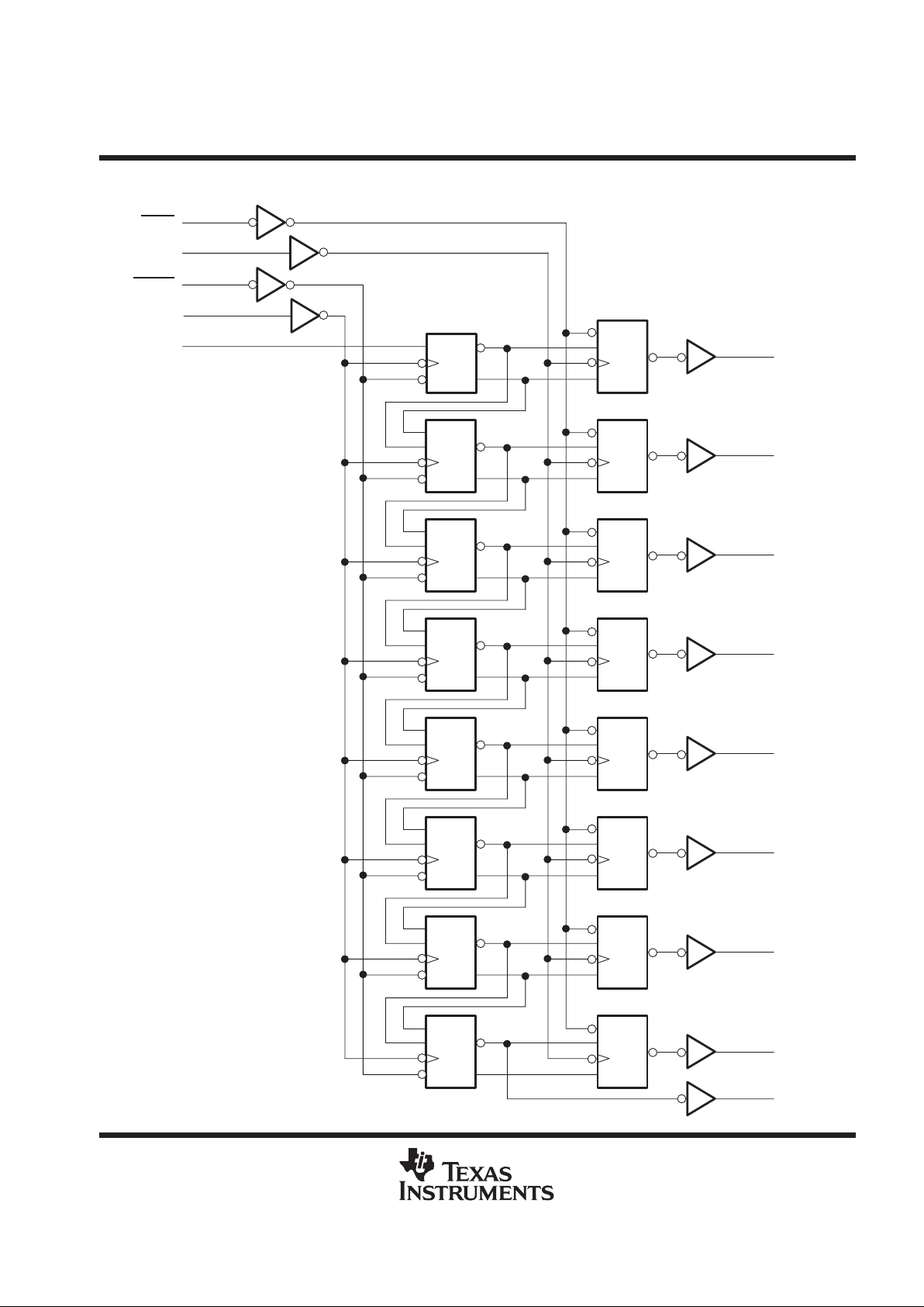
logic diagram (positive logic)
R
3R
C3
3S
1D
C1
R
R
3R
C3
3S
2R
C2
R
2S
R
3R
C3
3S
2R
C2
R
2S
R
3R
C3
3S
2R
C2
R
2S
R
3R
C3
3S
2R
C2
R
2S
R
3R
C3
3S
2R
C2
R
2S
R
3R
C3
3S
2R
C2
R
2S
R
3R
C3
3S
2R
C2
R
2S
13
12
10
11
14
15
1
2
3
4
5
6
7
9
Q
A
Q
B
Q
C
Q
D
Q
E
Q
F
Q
G
Q
H
Q
H′
RCLR
SRCLR
RCLK
SRCLK
SER
Pin numbers shown are for the D, DB, J, N, and W packages.
 Loading...