

Datasheet SN74HC373DBR, SN74HC373DW, SN74HC373DWR, SN74HC373N, SN74HC373NSR Datasheet (Texas Instruments)
...
SOIC
DW
HC373
TSSOP
PW
HC373
D
Wide Operating Voltage Range of 2 V to 6 V
D
High-Current 3-State True Outputs Can
Drive Up To 15 LSTTL Loads
D
Low Power Consumption, 80-µA Max I
D
Typical t
pd
= 13 ns
CC
SN54HC373, SN74HC373
OCTAL TRANSPARENT D-TYPE LATCHES
WITH 3-STATE OUTPUTS
SCLS140C – DECEMBER 1982 – REVISED DECEMBER 2002
D
±6-mA Output Drive at 5 V
D
Low Input Current of 1 µA Max
D
Eight High-Current Latches in a Single
Package
D
Full Parallel Access for Loading
SN54HC373 ...J OR W PACKAGE
SN74HC373 . . . DB, DW, N, NS, OR PW PACKAGE
OE
1Q
1D
2D
2Q
3Q
3D
4D
4Q
GND
(TOP VIEW)
1
20
2
19
3
18
4
17
5
16
6
15
7
14
8
13
9
12
10
11
V
8Q
8D
7D
7Q
6Q
6D
5D
5Q
LE
CC
SN54HC373 ...FK PACKAGE
2D
2Q
3Q
3D
4D
(TOP VIEW)
1D1QOE
3212019
4
5
6
7
8
910111213
4Q
LE
V
5Q
CC
8Q
18
17
16
15
14
5D
GND
description/ordering information
These 8-bit latches feature 3-state outputs designed specifically for driving highly capacitive or relatively
low-impedance loads. They are particularly suitable for implementing buffer registers, I/O ports, bidirectional
bus drivers, and working registers.
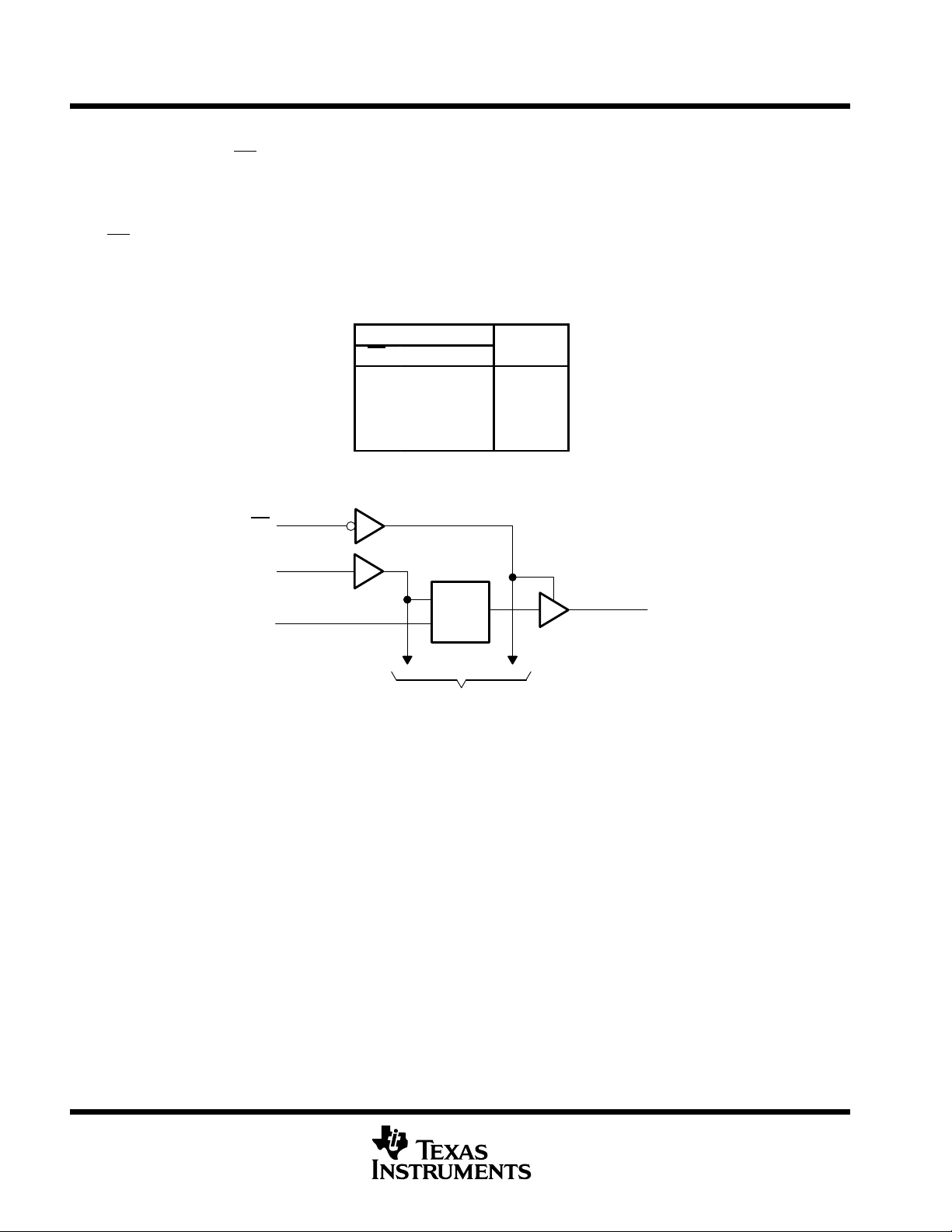
The eight latches of the ’HC373 devices are transparent D-type latches. While the latch-enable (LE) input is
high, the Q outputs follow the data (D) inputs. When LE is taken low, the Q outputs are latched at the levels that
were set up at the D inputs.
8D
7D
7Q
6Q
6D
T
A
PDIP – N Tube SN74HC373N SN74HC373N
–
–40°C to 85°C
–55°C to 125°C
†
Package drawings, standard packing quantities, thermal data, symbolization, and PCB design guidelines are
available at www.ti.com/sc/package.
Please be aware that an important notice concerning availability, standard warranty, and use in critical applications of
Texas Instruments semiconductor products and disclaimers thereto appears at the end of this data sheet.
PRODUCTION DATA information is current as of publication date.
Products conform to specifications per the terms of Texas Instruments
standard warranty. Production processing does not necessarily include
testing of all parameters.
SOP – NS Tape and reel SN74HC373NSR HC373
SSOP – DB Tape and reel SN74HC373DBR HC373
–
CDIP – J Tube SNJ54HC373J SNJ54HC373J
CFP – W Tube SNJ54HC373W SNJ54HC373W
LCCC – FK Tube SNJ54HC373FK SNJ54HC373FK
ORDERING INFORMA TION
PACKAGE
†
Tube SN74HC373DW
Tape and reel SN74HC373DWR
Tube SN74HC373PW
Tape and reel SN74HC373PWR
ORDERABLE
PART NUMBER
TOP-SIDE
MARKING
Copyright 2002, Texas Instruments Incorporated
On products compliant to MIL-PRF-38535, all parameters are tested
unless otherwise noted. On all other products, production
processing does not necessarily include testing of all parameters.
POST OFFICE BOX 655303 • DALLAS, TEXAS 75265
1
SN54HC373, SN74HC373
OCTAL TRANSPARENT D-TYPE LATCHES
WITH 3-STATE OUTPUTS
SCLS140C – DECEMBER 1982 – REVISED DECEMBER 2002
description/ordering information (continued)
An output-enable (OE) input places the eight outputs in either a normal logic state (high or low logic levels) or
the high-impedance state. In the high-impedance state, the outputs neither load nor drive the bus lines
significantly. The high-impedance state and increased drive provide the capability to drive bus lines without
interface or pullup components.
OE
does not affect the internal operations of the latches. Old data can be retained or new data can be entered
while the outputs are off.
FUNCTION TABLE
(each latch)
INPUTS
OE LE D
L H H H
L HL L
L LX Q
H X X Z
logic diagram (positive logic)
OUTPUT
Q
0
1
OE
11
LE
1D
3
To Seven Other Channels
C1
1D
2
1Q
absolute maximum ratings over operating free-air temperature range (unless otherwise noted)
Supply voltage range, V
Input clamp current, I
Output clamp current, I
Continuous output current, I
Continuous current through V
Package thermal impedance, θ
Storage temperature range, T
†
Stresses beyond those listed under “absolute maximum ratings” may cause permanent damage to the device. These are stress ratings only, and
functional operation of the device at these or any other conditions beyond those indicated under “recommended operating conditions” is not
implied. Exposure to absolute-maximum-rated conditions for extended periods may affect device reliability.
NOTES: 1. The input and output voltage ratings may be exceeded if the input and output current ratings are observed.
2. The package thermal impedance is calculated in accordance with JESD 51-7.
–0.5 V to 7 V. . . . . . . . . . . . . . . . . . . . . . . . . . . . . . . . . . . . . . . . . . . . . . . . . . . . . . . . . .
CC
(VI < 0 or VI > VCC) (see Note 1) ±20 mA. . . . . . . . . . . . . . . . . . . . . . . . . . . . . . . . . . . .
IK
(VO < 0 or VO > VCC) (see Note 1) ±20 mA. . . . . . . . . . . . . . . . . . . . . . . . . . . . . . . .
OK
(VO = 0 to VCC) ±35 mA. . . . . . . . . . . . . . . . . . . . . . . . . . . . . . . . . . . . . . . . . . . . . .
O
or GND ±70 mA. . . . . . . . . . . . . . . . . . . . . . . . . . . . . . . . . . . . . . . . . . . . . . . . . . .
CC
(see Note 2): DB package 70°C/W. . . . . . . . . . . . . . . . . . . . . . . . . . . . . . . . .
JA
DW package 58°C/W. . . . . . . . . . . . . . . . . . . . . . . . . . . . . . . . .
N package 69°C/W. . . . . . . . . . . . . . . . . . . . . . . . . . . . . . . . . . .
NS package 60°C/W. . . . . . . . . . . . . . . . . . . . . . . . . . . . . . . . .
PW package 83°C/W. . . . . . . . . . . . . . . . . . . . . . . . . . . . . . . . .
–65°C to 150°C. . . . . . . . . . . . . . . . . . . . . . . . . . . . . . . . . . . . . . . . . . . . . . . . . . .
stg
†
2
POST OFFICE BOX 655303 • DALLAS, TEXAS 75265
UNIT
PARAMETER
TEST CONDITIONS
V
UNIT
SN54HC373, SN74HC373
OCTAL TRANSPARENT D-TYPE LATCHES
WITH 3-STATE OUTPUTS
SCLS140C – DECEMBER 1982 – REVISED DECEMBER 2002
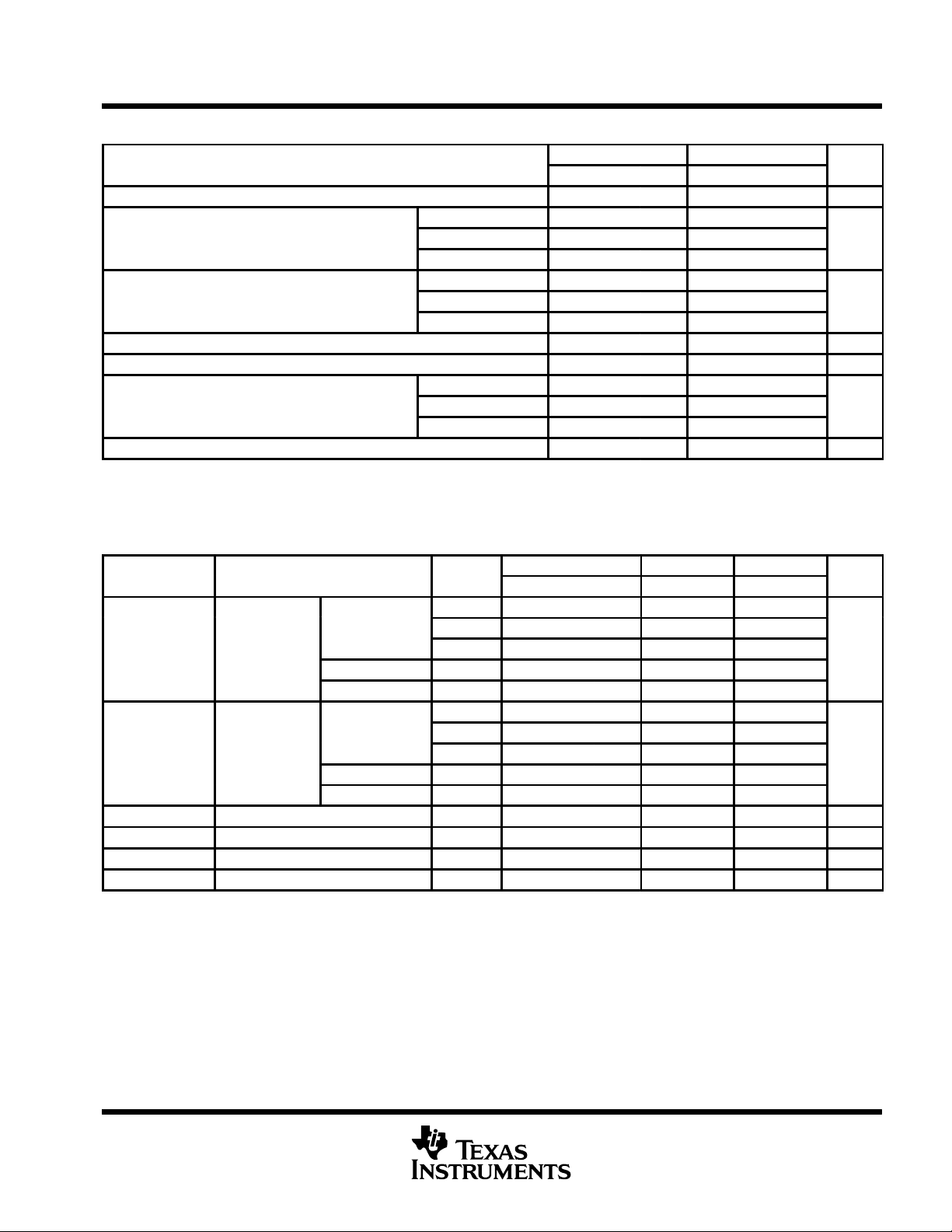
recommended operating conditions (see Note 3)
SN54HC373 SN74HC373
MIN NOM MAX MIN NOM MAX
V
V
V
V
V
∆t/∆v Input transition rise/fall time
T
NOTE 3: All unused inputs of the device must be held at VCC or GND to ensure proper device operation. Refer to the TI application report,
Supply voltage 2 5 6 2 5 6 V
CC
VCC = 2 V 1.5 1.5
High-level input voltage
IH
Low-level input voltage
IL
Input voltage 0 V
I
Output voltage 0 V
O
Operating free-air temperature –55 125 –40 85 °C
A
Implications of Slow or Floating CMOS Inputs, literature number SCBA004.
VCC = 4.5 V
VCC = 6 V 4.2 4.2
VCC = 2 V 0.5 0.5
VCC = 4.5 V
VCC = 6 V 1.8 1.8
VCC = 2 V 1000 1000
VCC = 4.5 V
VCC = 6 V 400 400
3.15 3.15
1.35 1.35
CC
CC
500 500
0 V
0 V
CC
CC
V
V
V
V
ns
electrical characteristics over recommended operating free-air temperature range (unless
otherwise noted)
TA = 25°C SN54HC373 SN74HC373
MIN TYP MAX MIN MAX MIN MAX
V
V
V
V
I
I
I
C
OH
OL
I
OZ
CC
i
CC
2 V 1.9 1.998 1.9 1.9
IOH = –20 µA
VI = VIH or V
VI = VIH or V
VI = VCC or 0 6 V ±0.1 ±100 ±1000 ±1000 nA
VO = VCC or 0 6 V ±0.01 ±0.5 ±10 ±5 µA
VI = VCC or 0, IO = 0 6 V 8 160 80 µA
IL
IOH = –6 mA 4.5 V 3.98 4.3 3.7 3.84
IOH = –7.8 mA 6 V 5.48 5.8 5.2 5.34
IOL = 20 µA
IL
IOL = 6 mA 4.5 V 0.17 0.26 0.4 0.33
IOL = 7.8 mA 6 V 0.15 0.26 0.4 0.33
4.5 V 4.4 4.499 4.4 4.4
6 V 5.9 5.999 5.9 5.9
2 V 0.002 0.1 0.1 0.1
4.5 V 0.001 0.1 0.1 0.1
6 V 0.001 0.1 0.1 0.1
2 V to 6 V 3 10 10 10 pF
POST OFFICE BOX 655303 • DALLAS, TEXAS 75265
3
SN54HC373, SN74HC373
V
UNIT
↓
↓
PARAMETER
V
UNIT
t
ns
OCTAL TRANSPARENT D-TYPE LATCHES
WITH 3-STATE OUTPUTS
SCLS140C – DECEMBER 1982 – REVISED DECEMBER 2002
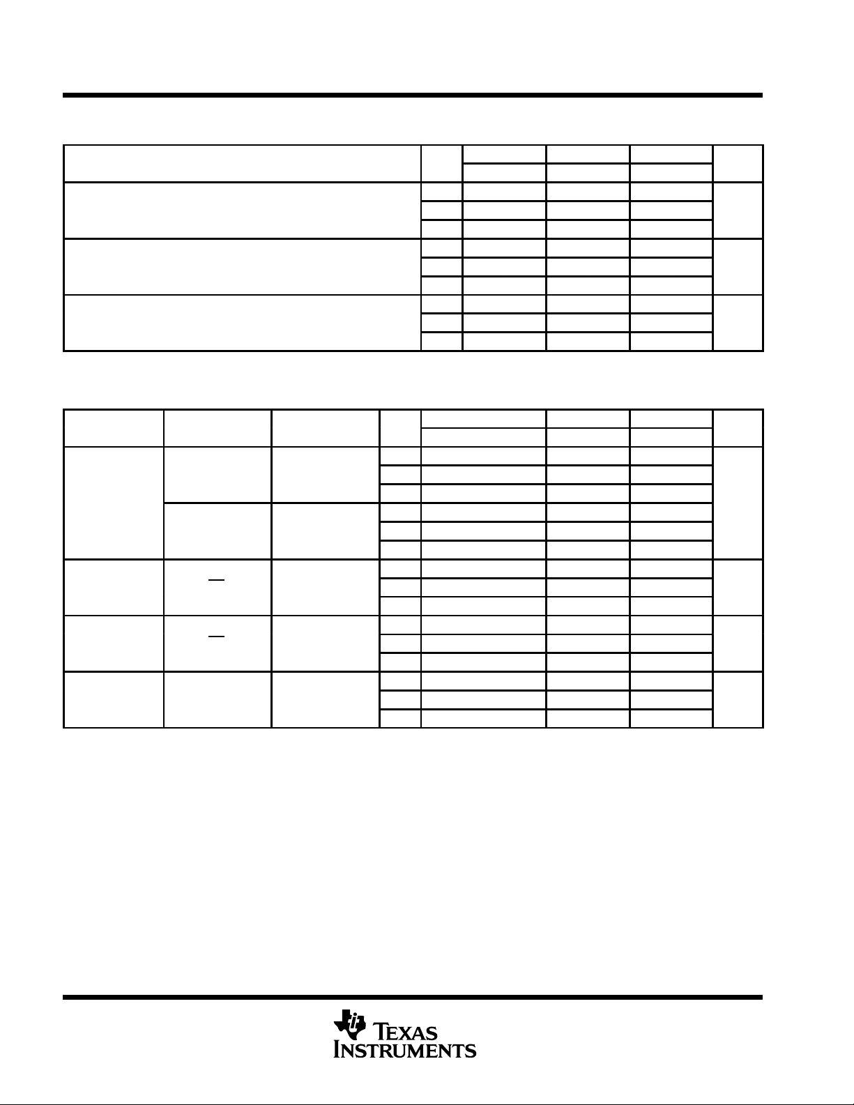
timing requirements over recommended operating free-air temperature range (unless otherwise
noted)
TA = 25°C SN54HC373 SN74HC373
CC
MIN MAX MIN MAX MIN MAX
2 V 80 120 100
t
w
t
su
t
h
switching characteristics over recommended operating free-air temperature range, CL = 50 pF
(unless otherwise noted) (see Figure 1)
Pulse duration, LE high
Setup time, data before LE
Hold time, data after LE
FROM TO
(INPUT) (OUTPUT)
pd
t
en
t
dis
t
t
D Q
LE Any Q
OE Any Q
OE Any Q
Any Q
4.5 V
6 V 14 20 17
2 V 50 75 63
4.5 V 10 15 13
6 V 9 13 11
2 V 20 26 24
4.5 V 10 13 12
6 V 10 13 12
CC
MIN TYP MAX MIN MAX MIN MAX
2 V 58 150 225 190
4.5 V 15 30 45 38
6 V 13 26 38 32
2 V 73 175 265 220
4.5 V 18 35 53 44
6 V 15 30 45 38
2 V 65 150 225 190
4.5 V 17 30 45 38
6 V 14 26 38 32
2 V 50 150 225 190
4.5 V 15 30 45 38
6 V 13 26 38 32
2 V 28 60 90 75
4.5 V 8 12 18 15
6 V 6 10 15 13
16 24 20
TA = 25°C SN54HC373 SN74HC373
ns
ns
ns
ns
ns
ns
4
POST OFFICE BOX 655303 • DALLAS, TEXAS 75265
PARAMETER
V
UNIT
t
ns
SN54HC373, SN74HC373
OCTAL TRANSPARENT D-TYPE LATCHES
WITH 3-STATE OUTPUTS
SCLS140C – DECEMBER 1982 – REVISED DECEMBER 2002
switching characteristics over recommended operating free-air temperature range, CL = 150 pF
(unless otherwise noted) (see Figure 1)
FROM TO
(INPUT) (OUTPUT)
D Q
pd
LE Any Q
t
en
t
t
OE Any Q
Any Q
operating characteristics, TA = 25°C
PARAMETER TEST CONDITIONS TYP UNIT
C
Power dissipation capacitance per latch No load 100 pF
pd
CC
2 V 82 200 300 250
4.5 V 22 40 60 50
6 V 19 34 51 43
2 V 100 225 335 285
4.5 V 24 45 67 57
6 V 20 38 57 48
2 V 90 200 300 250
4.5 V 23 40 60 50
6 V 19 34 51 43
2 V 45 210 315 265
4.5 V 17 42 63 53
6 V 13 36 53 45
TA = 25°C SN54HC373 SN74HC373
MIN TYP MAX MIN MAX MIN MAX
ns
ns
POST OFFICE BOX 655303 • DALLAS, TEXAS 75265
5

SN54HC373, SN74HC373
OCTAL TRANSPARENT D-TYPE LATCHES
WITH 3-STATE OUTPUTS
SCLS140C – DECEMBER 1982 – REVISED DECEMBER 2002
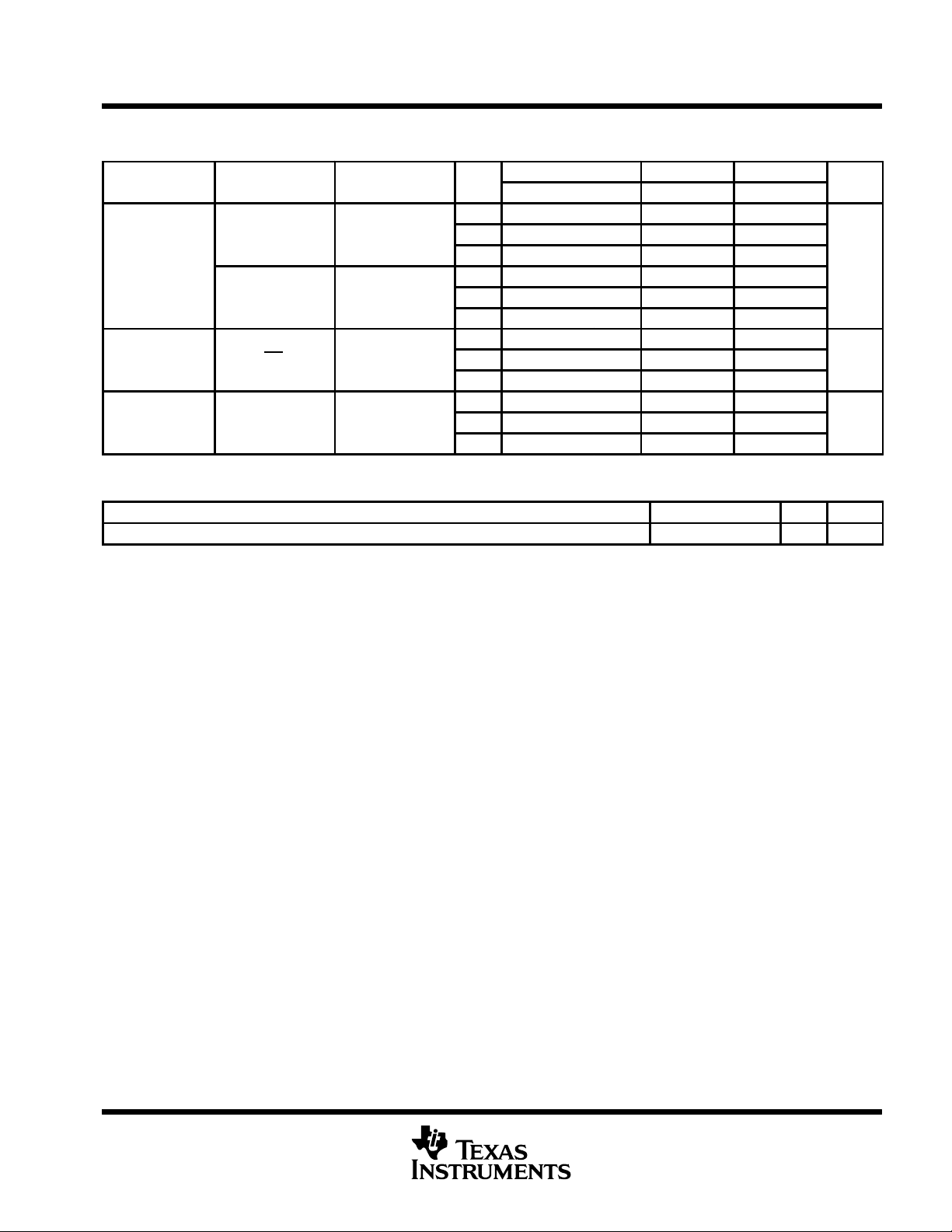
PARAMETER MEASUREMENT INFORMATION
V
CC
50%
50%
S1
S2
V
0 V
V
0 V
CC
CC
From Output
Under Test
(see Note A)
High-Level
Pulse
Low-Level
Pulse
Test
Point
C
L
LOAD CIRCUIT
50%
50%
VOLTAGE WAVEFORMS
PULSE DURATIONS
R
L
t
w
PARAMETER C
t
Input
Data
Input
t
PZH
t
PZL
t
PHZ
t
PLZ
t
en
t
dis
tpd or t
Reference
SETUP AND HOLD AND INPUT RISE AND FALL TIMES
R
L
1 kΩ
1 kΩ
t
su
90% 90%
VOLTAGE WAVEFORMS
t
r
L
50 pF
or
150 pF
50 pF
50 pF
or
150 pF
50%
S1
Open Closed
Closed Open
Open Closed
Closed Open
Open Open––
t
h
S2
V
CC
0 V
V
50%50%
CC
10%10%
0 V
t
f
Input
In-Phase
Output
Out-of-
Phase
Output
PROPAGATION DELAY AND OUTPUT TRANSITION TIMES
NOTES: A. CL includes probe and test-fixture capacitance.
50%
t
PLH
90% 90%
t
PHL
50% 50%
10% 10%
VOLTAGE WAVEFORMS
B. Waveform 1 is for an output with internal conditions such that the output is low except when disabled by the output control.
Waveform 2 is for an output with internal conditions such that the output is high except when disabled by the output control.
C. Phase relationships between waveforms were chosen arbitrarily. All input pulses are supplied by generators having the following
characteristics: PRR ≤ 1 MHz, ZO = 50 Ω, tr = 6 ns, tf = 6 ns.
D. The outputs are measured one at a time with one input transition per measurement.
E. t
F. t
G. t
PLZ
PZL
PLH
and t
and t
and t
are the same as t
PHZ
are the same as ten.
PZH
are the same as tpd.
PHL
50%
t
PHL
50%50%
t
r
t
PLH
t
f
.
dis
Figure 1. Load Circuit and Voltage Waveforms
V
CC
0 V
V
OH
10%10%
V
OL
t
f
V
OH
90%90%
V
OL
t
r
Output
Control
(Low-Level
Enabling)
t
PZL
Output
Waveform 1
(See Note B)
t
PZH
Output
Waveform 2
(See Note B)
ENABLE AND DISABLE TIMES FOR 3-STATE OUTPUTS
50%
≈V
CC
50%
50%
VOLTAGE WAVEFORMS
50%
t
PLZ
10%
t
PHZ
90%
V
CC
0 V
≈V
V
OL
V
OH
≈0 V
CC
6
POST OFFICE BOX 655303 • DALLAS, TEXAS 75265


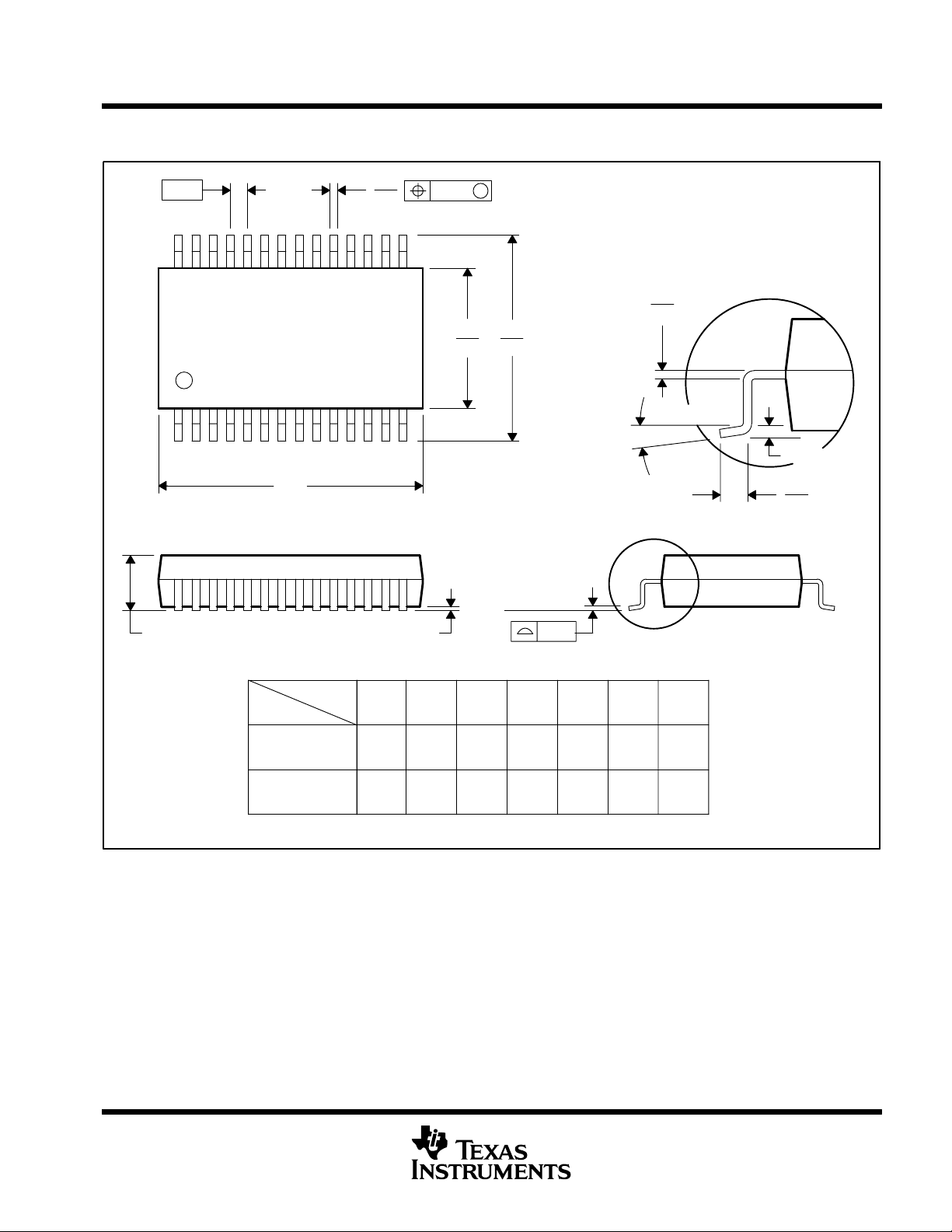
MECHANICAL DATA
MCFP006A– JANUARY 1995 – REVISED FEBRUARY 2002
W (R-GDFP-F20) CERAMIC DUAL FLATPACK
0.100 (2,54)
0.045 (1,14)
0.540 (13,72)
0.490 (12,45)
0.045 (1,14)
0.026 (0,66)
0.300 (7,62)
0.245 (6,22)
0.320 (8,13) MAX
Base and Seating Plane
0.006 (0,15)
0.004 (0,10)
201
0.019 (0,48)
0.015 (0,38)
0.050 (1,27)
10 11
0.260 (6,60)
0.200 (5,08)
NOTES: A. All linear dimensions are in inches (millimeters).
B. This drawing is subject to change without notice.
C. This package can be hermetically sealed with a ceramic lid using glass frit.
D. Index point is provided on cap for terminal identification only.
0.005 (0,13) MIN
4 Places
0.260 (6,60)
0.200 (5,08)
4040180-4/C 02/02
POST OFFICE BOX 655303 • DALLAS, TEXAS 75265
1

MECHANICAL DATA
MLCC006B – OCTOBER 1996
FK (S-CQCC-N**) LEADLESS CERAMIC CHIP CARRIER
28 TERMINAL SHOWN
A SQ
B SQ
19
20
21
22
23
24
25
12826 27
12
1314151618 17
0.020 (0,51)
0.010 (0,25)
MIN
0.342
(8,69)
0.442
0.640
0.739
0.938
1.141
A
0.358
(9,09)
0.458
(11,63)
0.660
(16,76)
0.761
(19,32)(18,78)
0.962
(24,43)
1.165
(29,59)
NO. OF
TERMINALS
**
11
10
9
8
7
6
5
432
20
28
44
52
68
84
0.020 (0,51)
0.010 (0,25)
(11,23)
(16,26)
(23,83)
(28,99)
MINMAX
0.307
(7,80)
0.406
(10,31)
0.495
(12,58)
0.495
(12,58)
0.850
(21,6)
1.047
(26,6)
0.080 (2,03)
0.064 (1,63)
B
MAX
0.358
(9,09)
0.458
(11,63)
0.560
(14,22)
0.560
(14,22)
0.858
(21,8)
1.063
(27,0)
0.055 (1,40)
0.045 (1,14)
0.028 (0,71)
0.022 (0,54)
0.050 (1,27)
NOTES: A. All linear dimensions are in inches (millimeters).
B. This drawing is subject to change without notice.
C. This package can be hermetically sealed with a metal lid.
D. The terminals are gold plated.
E. Falls within JEDEC MS-004
POST OFFICE BOX 655303 • DALLAS, TEXAS 75265
0.045 (1,14)
0.035 (0,89)
0.045 (1,14)
0.035 (0,89)
4040140/D 10/96
1

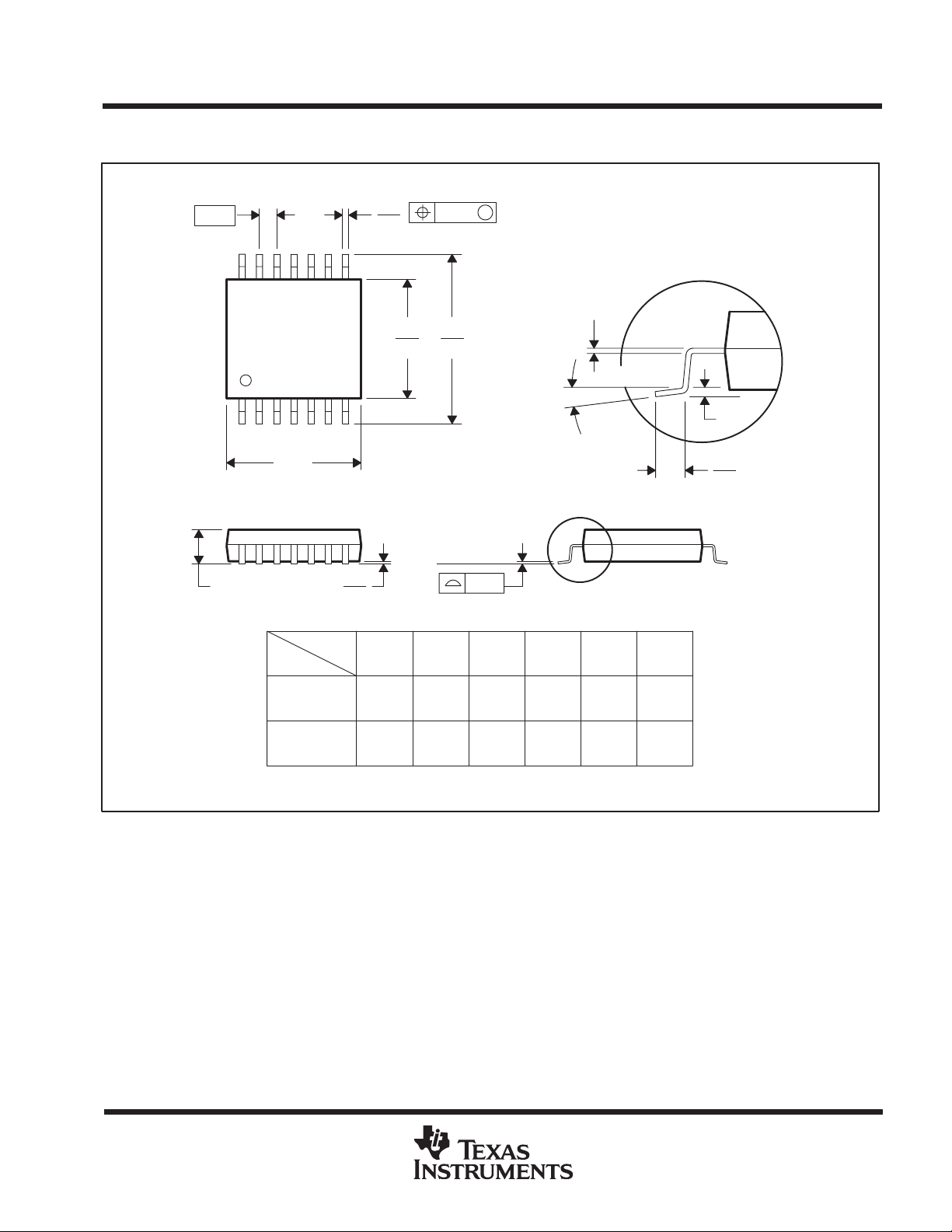
MECHANICAL
MPDI002C – JANUARY 1995 – REVISED DECEMBER 20002
N (R-PDIP-T**) PLASTIC DUAL-IN-LINE PACKAGE
16 PINS SHOWN
16
1
0.045 (1,14)
0.030 (0,76)
A
0.070 (1,78)
0.045 (1,14)
D
9
8
D
0.020 (0,51) MIN
0.260 (6,60)
0.240 (6,10)
0.200 (5,08) MAX
0.125 (3,18) MIN
DIM
A MAX
A MIN
C
Seating Plane
MS-100
VARIATION
PINS **
14
0.775
(19,69)
0.745
(18,92)
AA
0.325 (8,26)
0.300 (7,62)
16
0.775
(19,69)
0.745
(18,92)
BB AC AD
18
0.920
(23,37)
0.850
(21,59)
0.015 (0,38)
Gauge Plane
0.010 (0,25) NOM
20
1.060
(26,92)
0.940
(23,88)
0.100 (2,54)
0.021 (0,53)
0.015 (0,38)
0.010 (0,25)
NOTES: A. All linear dimensions are in inches (millimeters).
B. This drawing is subject to change without notice.
C. Falls within JEDEC MS-001, except 18 and 20 pin minimum body lrngth (Dim A).
D. The 20 pin end lead shoulder width is a vendor option, either half or full width.
M
14/18 PIN ONLY
20 pin vendor option
0.430 (10,92) MAX
D
4040049/E 12/2002
POST OFFICE BOX 655303 • DALLAS, TEXAS 75265
1

MECHANICAL DATA
MSOI003E – JANUARY 1995 – REVISED SEPTEMBER 2001
DW (R-PDSO-G**) PLASTIC SMALL-OUTLINE PACKAGE
16 PINS SHOWN
0.050 (1,27)
16
1
0.020 (0,51)
0.014 (0,35)
9
0.299 (7,59)
0.291 (7,39)
8
A
0.010 (0,25)
0.419 (10,65)
0.400 (10,15)
Seating Plane
0.010 (0,25) NOM
Gage Plane
0°– 8°
0.010 (0,25)
0.050 (1,27)
0.016 (0,40)
0.104 (2,65) MAX
NOTES: A. All linear dimensions are in inches (millimeters).
B. This drawing is subject to change without notice.
C. Body dimensions do not include mold flash or protrusion not to exceed 0.006 (0,15).
D. Falls within JEDEC MS-013
0.012 (0,30)
0.004 (0,10)
PINS **
DIM
A MAX
A MIN
0.004 (0,10)
16
0.410 0.462
(10,41)
0.400
(10,16)
18
(11,73)
0.453
(11,51)
20
0.510
(12,95)
0.500
24
0.610
(15,49)
0.600
(15,24)
28
0.710
(18,03)
0.700
(17,78)(12,70)
4040000/E 08/01
POST OFFICE BOX 655303 • DALLAS, TEXAS 75265
1

MECHANICAL DATA
MSSO002E – JANUARY 1995 – REVISED DECEMBER 2001
DB (R-PDSO-G**) PLASTIC SMALL-OUTLINE
28 PINS SHOWN
0,65
28
1
2,00 MAX
0,38
0,22
15
14
A
0,05 MIN
0,15
5,60
5,00
M
8,20
7,40
Seating Plane
0,10
0,25
0,09
0°–ā8°
Gage Plane
0,25
0,95
0,55
PINS **
DIM
A MAX
A MIN
NOTES: A. All linear dimensions are in millimeters.
B. This drawing is subject to change without notice.
C. Body dimensions do not include mold flash or protrusion not to exceed 0,15.
D. Falls within JEDEC MO-150
14
6,50
6,50
5,905,90
2016
7,50
6,90
24
8,50
28
10,50
9,907,90
30
10,50
9,90
38
12,90
12,30
4040065 /E 12/01
POST OFFICE BOX 655303 • DALLAS, TEXAS 75265
1
MECHANICAL DATA
MTSS001C – JANUARY 1995 – REVISED FEBRUARY 1999
PW (R-PDSO-G**) PLASTIC SMALL-OUTLINE PACKAGE
14 PINS SHOWN
0,65
1,20 MAX
14
0,30
0,19
8
4,50
4,30
PINS **
7
Seating Plane
0,15
0,05
8
1
A
DIM
14
0,10
6,60
6,20
M
0,10
0,15 NOM
0°–8°
2016
Gage Plane
24
0,25
0,75
0,50
28
A MAX
A MIN
NOTES: A. All linear dimensions are in millimeters.
B. This drawing is subject to change without notice.
C. Body dimensions do not include mold flash or protrusion not to exceed 0,15.
D. Falls within JEDEC MO-153
3,10
2,90
5,10
4,90
5,10
4,90
6,60
6,40
7,90
7,70
9,80
9,60
4040064/F 01/97
POST OFFICE BOX 655303 • DALLAS, TEXAS 75265
1

IMPORTANT NOTICE
Texas Instruments Incorporated and its subsidiaries (TI) reserve the right to make corrections, modifications,
enhancements, improvements, and other changes to its products and services at any time and to discontinue
any product or service without notice. Customers should obtain the latest relevant information before placing
orders and should verify that such information is current and complete. All products are sold subject to TI’s terms
and conditions of sale supplied at the time of order acknowledgment.
TI warrants performance of its hardware products to the specifications applicable at the time of sale in
accordance with TI’s standard warranty . Testing and other quality control techniques are used to the extent TI
deems necessary to support this warranty . Except where mandated by government requirements, testing of all
parameters of each product is not necessarily performed.
TI assumes no liability for applications assistance or customer product design. Customers are responsible for
their products and applications using TI components. T o minimize the risks associated with customer products
and applications, customers should provide adequate design and operating safeguards.
TI does not warrant or represent that any license, either express or implied, is granted under any TI patent right,
copyright, mask work right, or other TI intellectual property right relating to any combination, machine, or process
in which TI products or services are used. Information published by TI regarding third–party products or services
does not constitute a license from TI to use such products or services or a warranty or endorsement thereof.
Use of such information may require a license from a third party under the patents or other intellectual property
of the third party , or a license from TI under the patents or other intellectual property of TI.
Reproduction of information in TI data books or data sheets is permissible only if reproduction is without
alteration and is accompanied by all associated warranties, conditions, limitations, and notices. Reproduction
of this information with alteration is an unfair and deceptive business practice. TI is not responsible or liable for
such altered documentation.
Resale of TI products or services with statements different from or beyond the parameters stated by TI for that
product or service voids all express and any implied warranties for the associated TI product or service and
is an unfair and deceptive business practice. TI is not responsible or liable for any such statements.
Mailing Address:
Texas Instruments
Post Office Box 655303
Dallas, Texas 75265
Copyright 2003, Texas Instruments Incorporated
 Loading...