

Datasheet SN74HC161D, SN74HC161DBR, SN74HC161DR, SN74HC161N, SN74HC161N3 Datasheet (Texas Instruments)
...
SN54HC161, SN74HC161
4-BIT SYNCHRONOUS BINARY COUNTERS
SCLS297A – JANUARY 1996 – REVISED MA Y 1997
D
Internal Look-Ahead for Fast Counting
D
Carry Output for n-Bit Cascading
D
Synchronous Counting
D
Synchronously Programmable
D
Package Options Include Plastic
Small-Outline (D) and Ceramic Flat (W)
Packages, Ceramic Chip Carriers (FK), and
Standard Plastic (N) and Ceramic (J)
300-mil DIPs
description
These synchronous, presettable counters feature
an internal carry look-ahead for application in
high-speed counting designs. The ’HC161 are
4-bit binary counters. Synchronous operation is
provided by having all flip-flops clocked
simultaneously so that the outputs change
coincident with each other when so instructed by
the count-enable (ENP, ENT) inputs and internal
gating. This mode of operation eliminates the
output counting spikes that are normally
associated with synchronous (ripple-clock)
counters. A buffered clock (CLK) input triggers the
four flip-flops on the rising (positive-going) edge of
the clock waveform.
These counters are fully programmable; that is,
they can be preset to any number between 0 and
9 or 15. As presetting is synchronous, setting up
a low level at the load input disables the counter
and causes the outputs to agree with the setup
data after the next clock pulse, regardless of the
levels of the enable inputs.
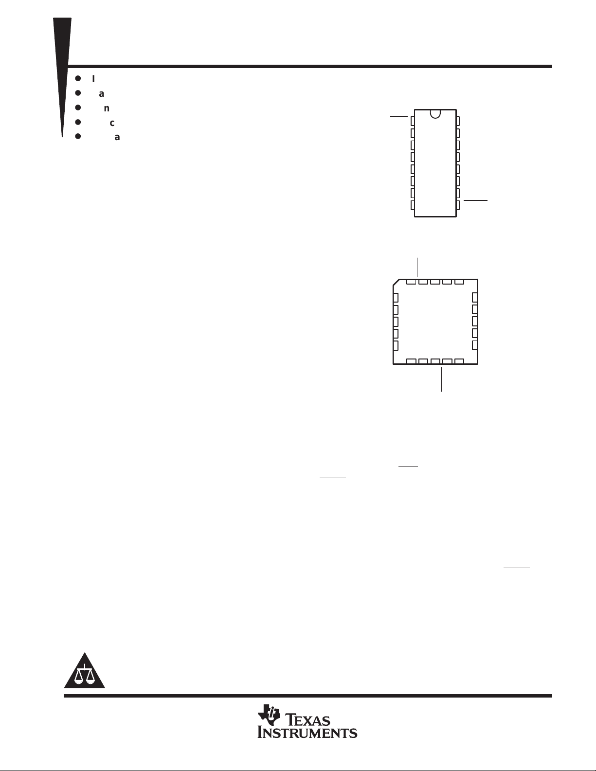
SN54HC161 ...J OR W PACKAGE
SN74HC161 . . . D OR N PACKAGE
SN54HC161 . . . FK PACKAGE
A
B
NC
C
D
NC – No internal connection
(TOP VIEW)
CLR
1
CLK
2
A
3
B
4
C
5
D
6
ENP
7
GND
8
(TOP VIEW)
CLK
3 2 1 20 19
4
5
6
7
8
910111213
ENP
CLR
GND
NC
NC
16
15
14
13
12
11
10
9
CC
V
LOAD
V
CC
RCO
Q
A
Q
B
Q
C
Q
D
ENT
LOAD
RCO
18
17
16
15
14
ENT
Q
Q
NC
Q
Q
A
B
C
D
The clear function for the ’HC161 is asynchronous. A low level at the clear (CLR
) input sets all four of the flip-flop
outputs low, regardless of the levels of the CLK, load (LOAD), or enable inputs.
The carry look-ahead circuitry provides for cascading counters for n-bit synchronous applications without
additional gating. Instrumental in accomplishing this function are ENP, ENT, and a ripple-carry output (RCO).
Both ENP and ENT must be high to count, and ENT is fed forward to enable RCO. Enabling RCO produces a
high-level pulse while the count is maximum (9 or 15 with Q
high). This high-level overflow ripple-carry pulse
A
can be used to enable successive cascaded stages. Transitions at ENP or ENT are allowed, regardless of the
level of CLK.
These counters feature a fully independent clock circuit. Changes at control inputs (ENP, ENT, or LOAD) that
modify the operating mode have no effect on the contents of the counter until clocking occurs. The function of
the counter (whether enabled, disabled, loading, or counting) is dictated solely by the conditions meeting the
stable setup and hold times.
The SN54HC161 is characterized for operation over the full military temperature range of –55°C to 125°C. The
SN74HC161 is characterized for operation from –40°C to 85°C.
Please be aware that an important notice concerning availability, standard warranty, and use in critical applications of
Texas Instruments semiconductor products and disclaimers thereto appears at the end of this data sheet.
PRODUCTION DATA information is current as of publication date.
Products conform to specifications per the terms of Texas Instruments
standard warranty. Production processing does not necessarily include
testing of all parameters.
POST OFFICE BOX 655303 • DALLAS, TEXAS 75265
Copyright 1997, Texas Instruments Incorporated
1
SN54HC161, SN74HC161
4-BIT SYNCHRONOUS BINARY COUNTERS
SCLS297A – JANUARY 1996 – REVISED MA Y 1997
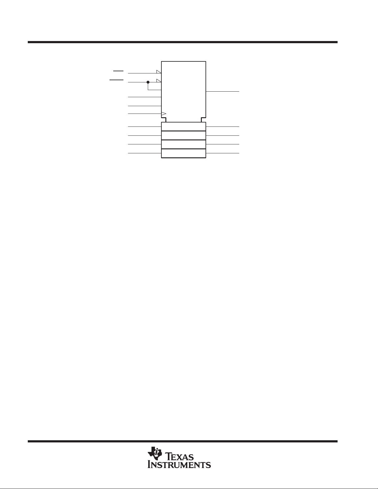
logic symbol
†
This symbol is in accordance with ANSI/IEEE Std 91-1984 and IEC Publication 617-12.
Pin numbers shown are for the D, J, N, and W packages.
†
CTRDIV16
CT=0
M1
M2
G3
G4
C5/2,3,4+
1,5D
3CT=15
[1]
[2]
[4]
[8]
CLR
LOAD
ENT
ENP
CLK
1
9
10
7
2
3
A
4
B
5
C
6
D
15
14
13
12
11
RCO
Q
A
Q
B
Q
C
Q
D
2
POST OFFICE BOX 655303 • DALLAS, TEXAS 75265
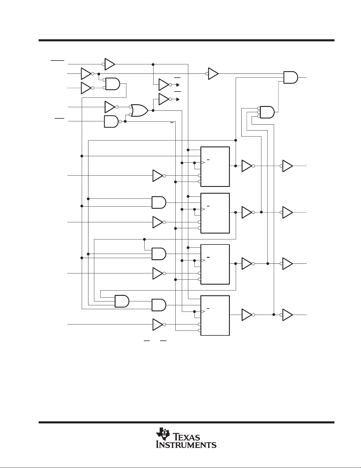
logic diagram (positive logic)
SN54HC161, SN74HC161
4-BIT SYNCHRONOUS BINARY COUNTERS
SCLS297A – JANUARY 1996 – REVISED MA Y 1997
LOAD
ENT
ENP
CLK
CLR
9
10
†
7
2
1
3
A
4
B
LD
†
CK
CK
R
LD
M1
G2
1
, 2T/1C3
G4
3D
4R
M1
G2
1
, 2T/1C3
G4
3D
4R
14
13
15
RCO
Q
A
Q
B
M1
G2
1
, 2T/1C3
5
C
6
D
†
For simplicity, routing of complementary signals LD and CK is not shown on this overall logic diagram. The uses of these signals are shown
on the logic diagram of the D/T flip-flops.
Pin numbers shown are for the D, J, N, and W packages.
G4
3D
4R
M1
G2
1
, 2T/1C3
G4
3D
4R
12
11
Q
C
Q
D
POST OFFICE BOX 655303 • DALLAS, TEXAS 75265
3
SN54HC161, SN74HC161
4-BIT SYNCHRONOUS BINARY COUNTERS
SCLS297A – JANUARY 1996 – REVISED MA Y 1997
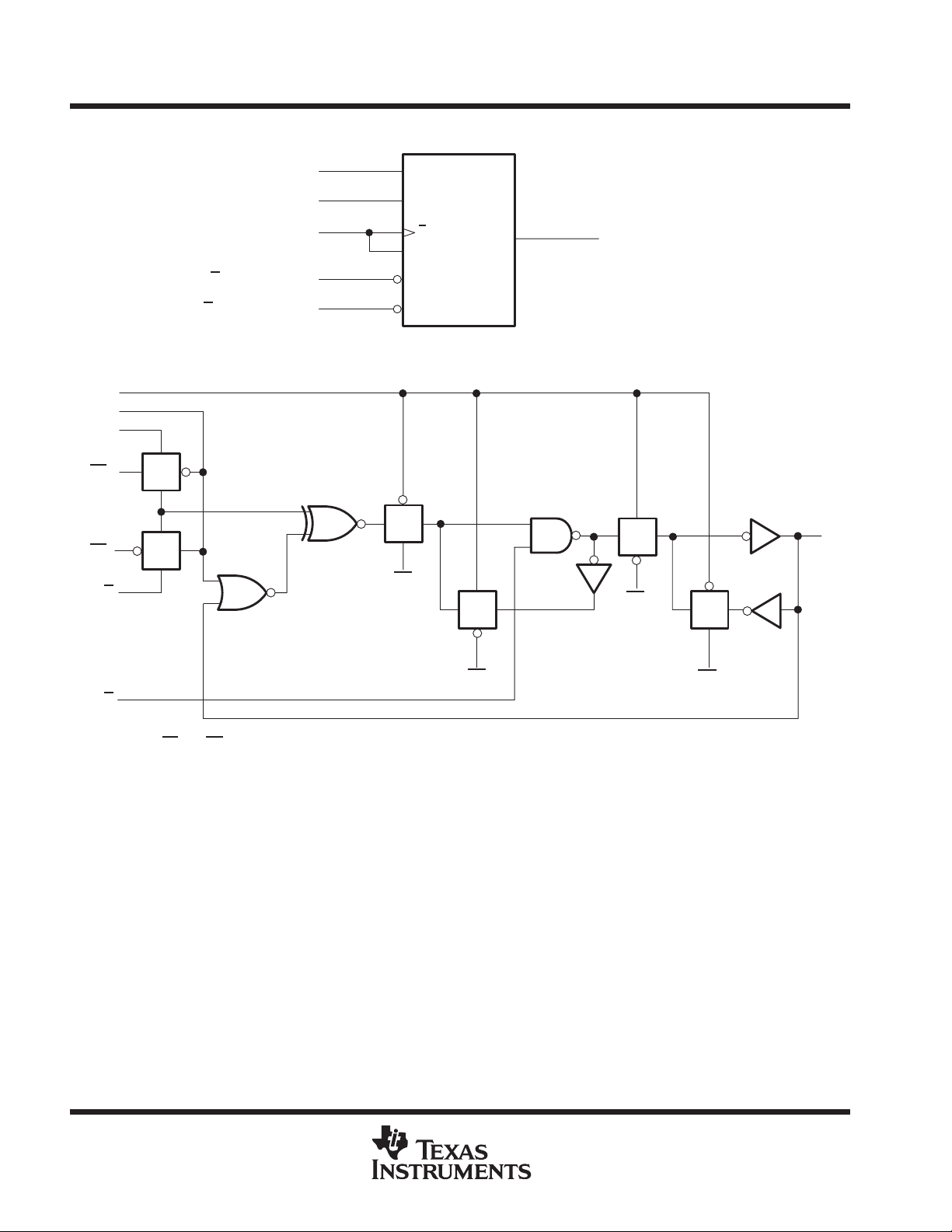
logic symbol, each D/T flip-flop
M1LD (Load)
G2TE (Toggle Enable)
CK (Clock)
D
(Inverted Data)
(Inverted Reset)
R
1, 2T/1C3
G4
3D
4R
logic diagram, each D/T flip-flop (positive logic)
CK
LD
TE
†
LD
LD
D
R
TG
TG
†
TG
†
CK
TG
CK
Q (Output)
TG
†
CK
†
TG
CK
†
Q
†
The origins of LD
4
and CK are shown in the logic diagram of the overall device.
POST OFFICE BOX 655303 • DALLAS, TEXAS 75265
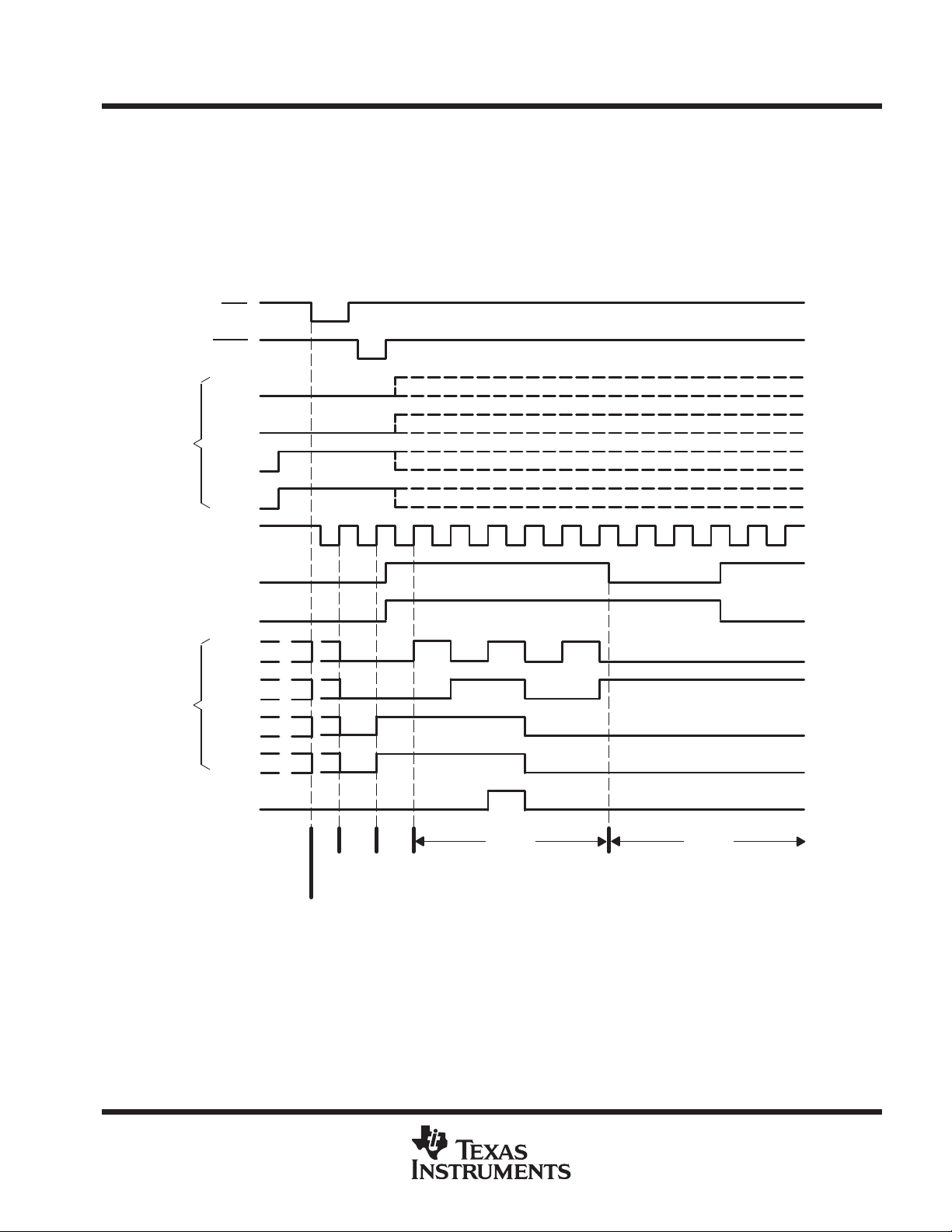
typical clear, preset, count, and inhibit sequence
The following sequence is illustrated below:
1. Clear outputs to zero (asynchronous)
2. Preset to binary 12
3. Count to 13, 14, 15, 0, 1, and 2
4. Inhibit
CLR
LOAD
A
SN54HC161, SN74HC161
4-BIT SYNCHRONOUS BINARY COUNTERS
SCLS297A – JANUARY 1996 – REVISED MA Y 1997
Data
Inputs
Data
Outputs
CLK
ENP
ENT
Q
Q
Q
Q
RCO
B
C
D
A
B
C
D
Sync
Clear
12 13
Preset
14 15 0 1 2
Count Inhibit
Async
Clear
POST OFFICE BOX 655303 • DALLAS, TEXAS 75265
5

SN54HC161, SN74HC161
UNIT
‡
4-BIT SYNCHRONOUS BINARY COUNTERS
SCLS297A – JANUARY 1996 – REVISED MA Y 1997
absolute maximum ratings over operating free-air temperature range
Supply voltage range, V
–0.5 V to 7 V. . . . . . . . . . . . . . . . . . . . . . . . . . . . . . . . . . . . . . . . . . . . . . . . . . . . . . . . . .
CC
†
Input clamp current, IIK (VI < 0 or VI > VCC) (see Note 1) ±20 mA. . . . . . . . . . . . . . . . . . . . . . . . . . . . . . . . . . . .
Output clamp current, IOK (VO < 0 or VO > VCC) (see Note 1) ±20 mA. . . . . . . . . . . . . . . . . . . . . . . . . . . . . . . .
Continuous output current, IO (VO = 0 to VCC) ±25 mA. . . . . . . . . . . . . . . . . . . . . . . . . . . . . . . . . . . . . . . . . . . . . .
Continuous current through VCC or GND ±50 mA. . . . . . . . . . . . . . . . . . . . . . . . . . . . . . . . . . . . . . . . . . . . . . . . . . .
Package thermal impedance, θ
(see Note 2): D package 113°C/W. . . . . . . . . . . . . . . . . . . . . . . . . . . . . . . . . .
JA
N package 78°C/W. . . . . . . . . . . . . . . . . . . . . . . . . . . . . . . . . . .
Storage temperature range, T
†
Stresses beyond those listed under “absolute maximum ratings” may cause permanent damage to the device. These are stress ratings only, and
functional operation of the device at these or any other conditions beyond those indicated under “recommended operating conditions” is not
implied. Exposure to absolute-maximum-rated conditions for extended periods may affect device reliability.
NOTES: 1. The input and output voltage ratings may be exceeded if the input and output current ratings are observed.
2. The package thermal impedance is calculated in accordance with JESD 51, except for through-hole packages, which use a trace
length of zero.
–65°C to 150°C. . . . . . . . . . . . . . . . . . . . . . . . . . . . . . . . . . . . . . . . . . . . . . . . . . .
stg
recommended operating conditions
SN54HC161 SN74HC161
MIN NOM MAX MIN NOM MAX
V
V
V
V
V
t
t
T
‡
If this device is used in the threshold region (from VILmax = 0.5 V to VIHmin = 1.5 V), there is a potential to go into the wrong state from induced
grounding, causing double clocking. Operating with the inputs at tt = 1000 ns and VCC = 2 V does not damage the device; however, functionally ,
the CLK inputs are not ensured while in the shift, count, or toggle operating modes.
Supply voltage 2 5 6 2 5 6 V
CC
VCC = 2 V 1.5 1.5
High-level input voltage
IH
Low-level input voltage
IL
Input voltage 0 V
I
Output voltage 0 V
O
Input transition (rise and fall) time
Operating free-air temperature –55 125 –40 85 °C
A
VCC = 4.5 V
VCC = 6 V 4.2 4.2
VCC = 2 V 0 0.5 0 0.5
VCC = 4.5 V
VCC = 6 V 0 1.8 0 1.8
VCC = 2 V 0 1000 0 1000
VCC = 4.5 V
VCC = 6 V 0 400 0 400
3.15 3.15
0 1.35 0 1.35
CC
CC
0 500 0 500
0 V
0 V
CC
CC
V
V
V
V
ns
6
POST OFFICE BOX 655303 • DALLAS, TEXAS 75265

PARAMETER
TEST CONDITIONS
V
UNIT
V
UNIT
twPulse duration
ns
tsuSetup time before CLK↑
ns
↑
SN54HC161, SN74HC161
4-BIT SYNCHRONOUS BINARY COUNTERS
SCLS297A – JANUARY 1996 – REVISED MA Y 1997
electrical characteristics over recommended operating free-air temperature range (unless
otherwise noted)
TA = 25°C SN54HC161 SN74HC161
MIN TYP MAX MIN MAX MIN MAX
V
V
V
V
I
I
C
OH
OL
I
CC
i
CC
2 V 1.9 1.998 1.9 1.9
IOH = –20 µA
VI = VIH or V
VI = VIH or V
VI = VCC or 0 6 V ±0.1 ±100 ±1000 ±1000 nA
VI = VCC or 0, IO = 0 6 V 8 160 80 µA
IL
IOH = –4 mA 4.5 V 3.98 4.3 3.7 3.84
IOH = –5.2 mA 6 V 5.48 5.8 5.2 5.34
IOL = 20 µA
IL
IOL = 4 mA 4.5 V 0.17 0.26 0.4 0.33
IOL = 5.2 mA 6 V 0.15 0.26 0.4 0.33
4.5 V 4.4 4.499 4.4 4.4
6 V 5.9 5.999 5.9 5.9
2 V 0.002 0.1 0.1 0.1
4.5 V 0.001 0.1 0.1 0.1
6 V 0.001 0.1 0.1 0.1
2 V to 6 V 3 10 10 10 pF
timing requirements over recommended operating free-air temperature range (unless otherwise
noted)
TA = 25°C SN54HC161 SN74HC161
CC
MIN MAX MIN MAX MIN MAX
2 V 0 6 0 4.2 0 5
f
clock
t
h
Clock frequency
p
Hold time, all synchronous inputs after CLK
CLK high or low
CLR low
A, B, C, or D
LOAD low
ENP, ENT
CLR inactive
4.5 V
6 V 0 36 0 25 0 29
2 V 80 120 100
4.5 V 16 24 20
6 V 14 20 17
2 V 80 120 100
4.5 V 16 24 20
6 V 14 20 17
2 V 150 225 190
4.5 V 30 45 38
6 V 26 38 32
2 V 135 205 170
4.5 V 27 41 34
6 V 23 35 29
2 V 170 255 215
4.5 V 34 51 43
6 V 29 43 37
2 V 125 190 155
4.5 V 25 38 31
6 V 21 32 26
2 V 0 0 0
4.5 V 0 0 0
6 V 0 0 0
0 31 0 21 0 25
MHz
ns
POST OFFICE BOX 655303 • DALLAS, TEXAS 75265
7

SN54HC161, SN74HC161
PARAMETER
V
UNIT
CLK
t
CLR
ns
4-BIT SYNCHRONOUS BINARY COUNTERS
SCLS297A – JANUARY 1996 – REVISED MA Y 1997
switching characteristics over recommended operating free-air temperature range, CL = 50 pF
(unless otherwise noted) (see Figure 1)
TA = 25°C SN54HC161 SN74HC161
MIN TYP MAX MIN MAX MIN MAX
MHz
ns
ns
f
max
t
pd
PHL
t
t
FROM TO
(INPUT) (OUTPUT)
RCO
Any Q
ENT RCO
Any Q
RCO
Any
CC
2 V 6 14 4.2 5
4.5 V 31 40 21 25
6 V 36 44 25 29
2 V 83 215 325 270
4.5 V 24 43 65 54
6 V 20 37 55 46
2 V 80 205 310 255
4.5 V 25 41 62 51
6 V 21 35 53 43
2 V 62 195 295 245
4.5 V 17 39 59 49
6 V 14 33 50 42
2 V 105 210 315 265
4.5 V 21 42 63 53
6 V 18 36 54 45
2 V 110 220 330 275
4.5 V 22 44 66 55
6 V 19 37 56 47
2 V 38 75 110 95
4.5 V 8 15 22 19
6 V 6 13 19 16
operating characteristics, TA = 25°C
PARAMETER TEST CONDITIONS TYP UNIT
C
Power dissipation capacitance No load 60 pF
pd
8
POST OFFICE BOX 655303 • DALLAS, TEXAS 75265

PARAMETER MEASUREMENT INFORMATION
50%
Test
Point
CL = 50 pF
(see Note A)
t
h
50%50%
From Output
Under Test
LOAD CIRCUIT
Reference
Input
t
su
Data
Input
SETUP AND HOLD AND INPUT RISE AND FALL TIMES
90% 90%
t
r
VOLTAGE WAVEFORMS
SN54HC161, SN74HC161
4-BIT SYNCHRONOUS BINARY COUNTERS
SCLS297A – JANUARY 1996 – REVISED MA Y 1997
V
0 V
V
0 V
CC
CC
V
CC
0 V
V
50%50%
OH
10%10%
V
OL
t
f
V
OH
90%90%
V
OL
t
r
High-Level
Pulse
Low-Level
Pulse
Input
V
CC
0 V
V
CC
10%10%
0 V
t
f
In-Phase
Output
Out-of-Phase
Output
PROPAGATION DELAY AND OUTPUT TRANSITION TIMES
50%
t
t
PLH
PHL
50%
t
w
50%
VOLTAGE WAVEFORMS
PULSE DURATIONS
90% 90%
t
r
50% 50%
10% 10%
t
f
VOLTAGE WAVEFORMS
50%
t
50%
50%
t
PHL
PLH
NOTES: A. CL includes probe and test-fixture capacitance.
B. Phase relationships between waveforms were chosen arbitrarily. All input pulses are supplied by generators having the following
characteristics: PRR ≤ 1 MHz, ZO = 50 Ω, tr = 6 ns, tf = 6 ns.
C. For clock inputs, f
D. The outputs are measured one at a time with one input transition per measurement.
E. t
PLH
and t
PHL
is measured when the input duty cycle is 50%.
max
are the same as tpd.
Figure 1. Load Circuit and Voltage Waveforms
POST OFFICE BOX 655303 • DALLAS, TEXAS 75265
9

SN54HC161, SN74HC161
4-BIT SYNCHRONOUS BINARY COUNTERS
SCLS297A – JANUARY 1996 – REVISED MA Y 1997
APPLICATION INFORMATION
n-bit synchronous counters
This application demonstrates how the look-ahead carry circuit can be used to implement a high-speed n-bit
counter. The ’HC161 count in binary. Virtually any count mode (modulo-N, N1-to-N2, N1-to-maximum) can be
used with this fast look-ahead circuit.
The application circuit shown in Figure 2 is not valid for clock frequencies above 18 MHz (at 25°C and
4.5-V VCC). The reason for this is that there is a glitch that is produced on the second stage’s RCO and every
succeeding stage’s RCO. This glitch is common to all HC vendors that Texas Instruments has evaluated, in
addition to the bipolar equivalents (LS, ALS, AS).
10
POST OFFICE BOX 655303 • DALLAS, TEXAS 75265

SN54HC161, SN74HC161
4-BIT SYNCHRONOUS BINARY COUNTERS
SCLS297A – JANUARY 1996 – REVISED MA Y 1997
LSB
Clear (L)
Count (H)/
Disable (L)
CLR
LOAD
ENT
ENP
CLK
CTR
CT=0
M1
G3
G4
C5/2,3,4+
3CT=MAX
RCO
Load (L)
Count (H)/
Disable (L)
Clock
B
C
D
B
C
D
B
C
D
CLR
LOAD
ENT
ENP
CLK
CLR
LOAD
ENT
ENP
CLK
1,5DA
CTR
CT=0
M1
G3
G4
C5/2,3,4+
1,5DA
CTR
CT=0
M1
G3
G4
C5/2,3,4+
1,5DA
[1]
[2]
[3]
[4]
3CT=MAX
[1]
[2]
[3]
[4]
3CT=MAX
[1]
[2]
[3]
[4]
RCO
RCO
Q
A
Q
B
Q
C
Q
D
Q
A
Q
B
Q
C
Q
D
Q
A
Q
B
Q
C
Q
D
CLR
LOAD
ENT
ENP
CLK
B
C
D
To More Significant Stages
CTR
CT=0
M1
G3
G4
C5/2,3,4+
1,5DA
3CT=MAX
[1]
[2]
[3]
[4]
Figure 2
POST OFFICE BOX 655303 • DALLAS, TEXAS 75265
RCO
Q
A
Q
B
Q
C
Q
D
11

SN54HC161, SN74HC161
4-BIT SYNCHRONOUS BINARY COUNTERS
SCLS297A – JANUARY 1996 – REVISED MA Y 1997
The glitch on RCO is caused because the propagation delay of the rising edge of QA of the second stage is
shorter than the propagation delay of the falling edge of ENT . RCO is the product of ENT, QA, QB, QC, and Q
(ENT × QA × QB × QC × QD). The resulting glitch is about 7–12 ns in duration. Figure 3 shows the condition in
which the glitch occurs. For simplicity , only two stages are being considered, but the results can be applied to
other stages. Q
zero (1110 1110) after the first clock pulse. On the rising edge of the second clock pulse, QA and RCO of the
first stage go high. On the rising edge of the third clock pulse, QA and RCO of the first stage return to a low level,
and QA of the second stage goes to a high level. At this time, the glitch on RCO of the second stage appears
because of the race condition inside the chip.
, QC, and QD of the first and second stage are at logic one, and QA of both stages are at logic
B
12345
CLK
ENT1
D
QB1, QC1, Q
RCO1, ENT2
QB2, QC2, Q
D1
Q
A1
D2
Q
A2
RCO2
Glitch (7–12 ns)
Figure 3
The glitch causes a problem in the next stage (stage three) if the glitch is still present when the next rising clock
edge appears (clock pulse 4). To ensure that this does not happen, the clock frequency must be less than the
inverse of the sum of the clock-to-RCO propagation delay and the glitch duration (t
f
= 1/(tpdCLK-to-RCO + tg). For example, at 25°C at 4.5-V VCC, the clock-to-RCO propagation delay is
max
). In other words,
g
43 ns and the maximum duration of the glitch is 12 ns. Therefore, the maximum clock frequency that the
cascaded counters can use is 18 MHz. The following tables contain the f
clock
, tw, and f
specifications for
max
applications that use more than two ’HC161 devices cascaded together.
12
POST OFFICE BOX 655303 • DALLAS, TEXAS 75265

V
UNIT
PARAMETER
V
UNIT
SN54HC161, SN74HC161
4-BIT SYNCHRONOUS BINARY COUNTERS
SCLS297A – JANUARY 1996 – REVISED MA Y 1997
timing requirements over recommended operating free-air temperature range (unless otherwise
noted)
TA = 25°C SN54HC161 SN74HC161
CC
MIN MAX MIN MAX MIN MAX
2 V 0 3.6 0 2.5 0 2.9
f
clock
t
w
switching characteristics over recommended operating free-air temperature range, CL = 50 pF
(unless otherwise noted) (see Note 3)
NOTE 3: These limits apply only to applications that use more than two ’HC161 devices cascaded together.
Clock frequency
Pulse duration, CLK high or low
FROM TO
(INPUT) (OUTPUT)
f
max
4.5 V
6 V 0 21 0 14 0 17
2 V 140 200 170
4.5 V
6 V 24 36 30
CC
2 V 3.6 2.5 2.9
4.5 V 18 12 14
6 V 21 14 17
0 18 0 12 0 14
28 40 36
TA = 25°C SN54HC161 SN74HC161
MIN MAX MIN MAX MIN MAX
MHz
ns
MHz
If the ’HC161 are used as a single unit, or only two cascaded together, then the maximum clock frequency that
the device can use is not limited because of the glitch. In these situations, the device can be operated at the
maximum specifications.
A glitch can appear on RCO of a single ’HC161 device, depending on the relationship of ENT to CLK. Any
application that uses RCO to drive any input except an ENT of another cascaded ’HC161 must take this
into consideration.
POST OFFICE BOX 655303 • DALLAS, TEXAS 75265
13

IMPORTANT NOTICE
T exas Instruments and its subsidiaries (TI) reserve the right to make changes to their products or to discontinue
any product or service without notice, and advise customers to obtain the latest version of relevant information
to verify, before placing orders, that information being relied on is current and complete. All products are sold
subject to the terms and conditions of sale supplied at the time of order acknowledgement, including those
pertaining to warranty, patent infringement, and limitation of liability.
TI warrants performance of its semiconductor products to the specifications applicable at the time of sale in
accordance with TI’s standard warranty. Testing and other quality control techniques are utilized to the extent
TI deems necessary to support this warranty . Specific testing of all parameters of each device is not necessarily
performed, except those mandated by government requirements.
CERTAIN APPLICATIONS USING SEMICONDUCTOR PRODUCTS MAY INVOLVE POTENTIAL RISKS OF
DEATH, PERSONAL INJURY, OR SEVERE PROPERTY OR ENVIRONMENTAL DAMAGE (“CRITICAL
APPLICATIONS”). TI SEMICONDUCTOR PRODUCTS ARE NOT DESIGNED, AUTHORIZED, OR
WARRANTED TO BE SUITABLE FOR USE IN LIFE-SUPPORT DEVICES OR SYSTEMS OR OTHER
CRITICAL APPLICA TIONS. INCLUSION OF TI PRODUCTS IN SUCH APPLICATIONS IS UNDERST OOD TO
BE FULLY AT THE CUSTOMER’S RISK.
In order to minimize risks associated with the customer’s applications, adequate design and operating
safeguards must be provided by the customer to minimize inherent or procedural hazards.
TI assumes no liability for applications assistance or customer product design. TI does not warrant or represent
that any license, either express or implied, is granted under any patent right, copyright, mask work right, or other
intellectual property right of TI covering or relating to any combination, machine, or process in which such
semiconductor products or services might be or are used. TI’s publication of information regarding any third
party’s products or services does not constitute TI’s approval, warranty or endorsement thereof.
Copyright 1998, Texas Instruments Incorporated
 Loading...