

Texas Instruments SN74GTLPH16612DL, SN74GTLPH16612DLR, SN74GTLPH16612GR Datasheet
SN74GTLPH16612
18-BIT LVTTL-TO-GTLP UNIVERSAL BUS TRANSCEIVER
SCES326 – MARCH 2000
1
POST OFFICE BOX 655303 • DALLAS, TEXAS 75265
D
Members of the Texas Instruments (TI)
Widebus
Family
D
UBT
(Universal Bus Transceiver)
Combines D-Type Latches and D-Type
Flip-Flops for Operation in Transparent,
Latched, Clocked, or Clock-Enabled Mode
D
Translate Between GTLP Signal Levels and
LVTTL Logic Levels
D
Support Mixed-Mode (3.3 V and 5 V) Signal
Operation on A-Port and Control Inputs
D
B-Port Transition Time Optimized for
Distributed Backplane Loads
D
I
off
Supports Partial-Power-Down Mode
Operation
D
Bus Hold on A-Port Inputs Eliminates the
Need for External Pullup/Pulldown
Resistors
D
Distributed VCC and GND Pins Minimize
High-Speed Switching Noise
D
ESD Protection Exceeds JESD 22
– 2000-V Human-Body Model (A114-A)
– 200-V Machine Model (A115-A)
– 1000-V Charged-Device Model (C101)
D
Latch-Up Performance Exceeds 100 mA Per
JESD 78, Class II
D
Package Options Include Plastic Shrink
Small-Outline (DL), and Thin Shrink
Small-Outline (DGG) Packages
NOTE: For tape and reel order entry:
The DGGR package is abbreviated to GR.
description
The SN74GTLPH16612 is a medium-drive, 18-bit UBT (universal bus transceiver) that provides
LVTTL-to-GTLP and GTLP-to-LVTTL signal-level translation. It allows for transparent, latched, clocked, or
clock-enabled modes of data transfer. This device provides a high-speed interface between cards operating at
LVTTL logic levels and backplanes operating at GTLP signal levels. High-speed (about two times faster than
standard L VTTL or TTL) backplane operation is a direct result of the reduced output swing (<1 V), reduced input
threshold levels, and OEC (output edge control). These improvements minimize bus settling time and have
been designed and tested using several backplane models.
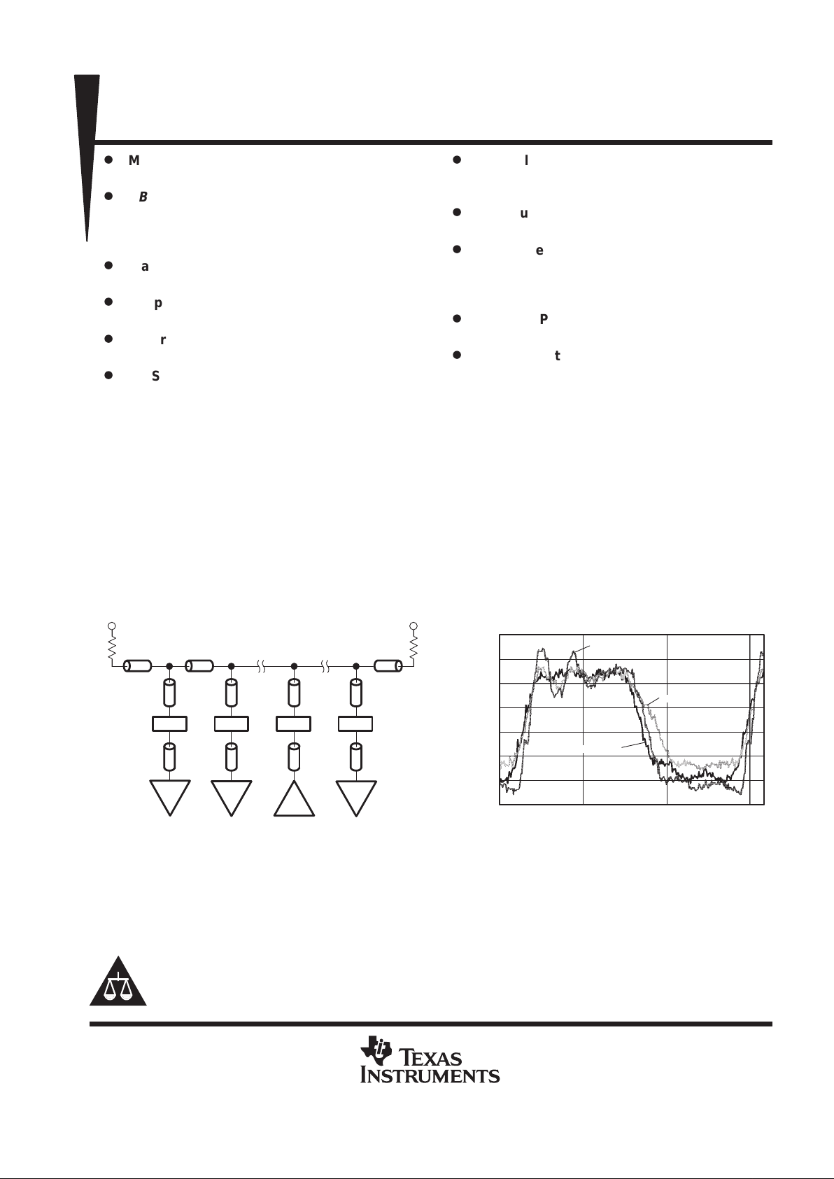
Drvr
V
TT
Conn.
.25”
.875”
.625” .625”
1” 1”
Slot 1 Slot 2
V
TT
.625”.625”
1”1”
Slot 16
Slot 8
.25”
R
TT
Conn. Conn. Conn.
Rcvr
Rcvr
Rcvr
R
TT
Volts – V
t – Time – ns
10 30
1.8
1.6
1.4
1.2
1.0
0.8
0.6
0.4
020
TI GTLPH16612
Fairchild GTLP16612
TI GTL16612
Figure 1. Test Backplane Model With Output Waveform Results
Copyright 2000, Texas Instruments Incorporated
Please be aware that an important notice concerning availability, standard warranty, and use in critical applications of
Texas Instruments semiconductor products and disclaimers thereto appears at the end of this data sheet.
TI, OEC, UBT, and Widebus are trademarks of Texas Instruments.
PRODUCTION DATA information is current as of publication date.
Products conform to specifications per the terms of Texas Instruments
standard warranty. Production processing does not necessarily include
testing of all parameters.
SN74GTLPH16612
18-BIT LVTTL-TO-GTLP UNIVERSAL BUS TRANSCEIVER
SCES326 – MARCH 2000
2
POST OFFICE BOX 655303 • DALLAS, TEXAS 75265
description (continued)
Figure 1 shows actual device output waveforms using a synchronous clock at 75 MHz. The test backplane is
a 16-slot, 14-inch board with loaded impedance of 33 Ω. VTT is 1.5 V , V
REF
is 1 V , and RTT pullup resistor is 50 Ω.
The driver is in slot 8, with receivers in alternate slots 1, 3, 5, 7, 10, 12, 14, and 16. Receiver slot 1 signals are
shown. The signal becomes progressively worse as the receiver moves closer to the driver or the spacing
between receiver cards is reduced. The clock is independent of the data and the system clock frequency is
limited by the backplane flight time to about 80 MHz to 90 MHz. This frequency can be increased even more
(30% to 40%) if the clock is generated and transmitted together with the data from the driver card (source
synchronous).
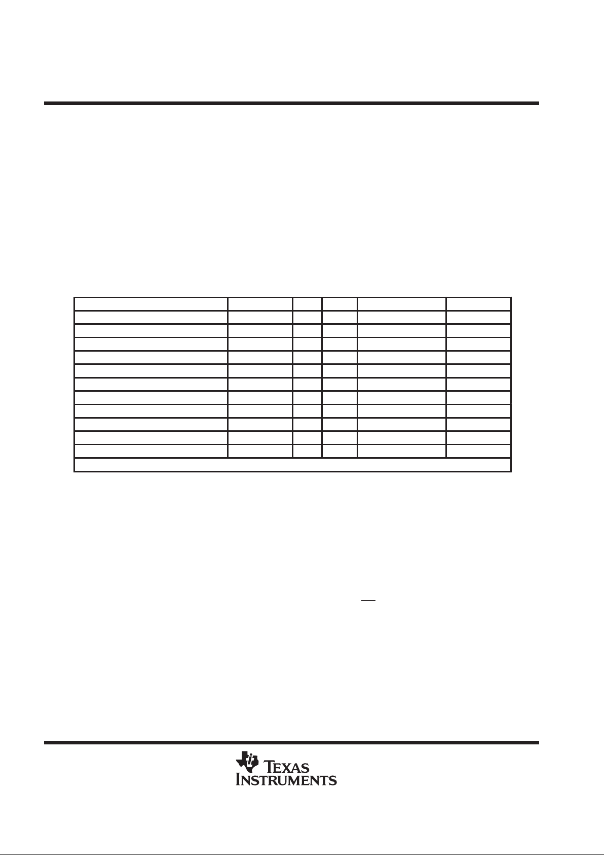
The SN74GTLPH16612 is a medium-drive (34 mA), 18-bit universal bus transceiver, containing D-type latches
and D-type flip-flops to allow data flow in transparent, latched, clocked, and clock-enabled modes. This UBT
can replace any of the functions shown in Table 1.
Table 1. SN74GTLPH16612 UBT Replacement Functions
FUNCTION 8 BIT 9 BIT 10 BIT 16 BIT 18 BIT
Transceiver ’245, ’623, ’645 ’863 ’861 ’16245, ’16623 ’16863
Buffer/driver ’241, ’244, ’541 ’827 ’16241, ’16244, ’16541 ’16825
Latched transceiver ’543 ’16543 ’16472
Latch ’373, ’573 ’843 ’841 ’16373 ’16843
Registered transceiver ’646, ’652 ’16646, ’16652 ’16474
Flip-flop ’374, ’574 ’821 ’16374
Standard UBT ’16500, ’16501
Universal bus driver ’16835
Registered transceiver with CLK enable ’2952 ’16470, ’16952
Flip-flop with CLK enable ’377 ’823 ’16823
Standard UBT with CLK enable ’16600, ’16601
SN74GTLPH16612 UBT replaces all above functions
GTLP is a TI derivative of the Gunning transceiver logic (GTL) JEDEC standard JESD 8-3. The ac specification
of the SN74GTLPH16612 is given only at the preferred higher noise-margin GTLP , but this device can be used
at either GTL (VTT = 1.2 V and V
REF
= 0.8 V) or GTLP (V
TT
= 1.5 V and V
REF
= 1 V) signal levels.
The B port normally operates at GTLP levels, while the A-port and control inputs are compatible with LVTTL
logic levels and are 5-V tolerant. V
REF
is the reference input voltage for the B port.
To improve signal integrity, the SN74GTLPH16612 B-port output transition time is optimized for distributed
backplane loads.
VCC (5 V) supplies the internal and GTLP circuitry, while VCC (3.3 V) supplies the LVTTL output buffers.
T o ensure the high-impedance state during power up or power down, OE
should be tied to VCC through a pullup
resistor; the minimum value of the resistor is determined by the current-sinking capability of the driver.
Active bus-hold circuitry holds unused or undriven L VTTL inputs at a valid logic state. Use of pullup or pulldown
resistors with the bus-hold circuitry is not recommended.
This device is fully specified for partial-power-down applications using I
off
. The I
off
circuitry disables the outputs,
preventing damaging current backflow through the device when it is powered down.
The SN74GTLPH16612 is characterized for operation from –40°C to 85°C.
SN74GTLPH16612
18-BIT LVTTL-TO-GTLP UNIVERSAL BUS TRANSCEIVER
SCES326 – MARCH 2000
3
POST OFFICE BOX 655303 • DALLAS, TEXAS 75265
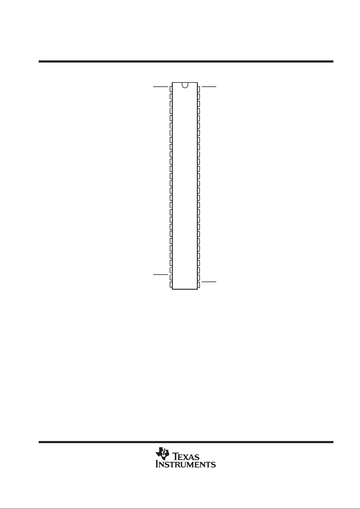
1
2
3
4
5
6
7
8
9
10
11
12
13
14
15
16
17
18
19
20
21
22
23
24
25
26
27
28
56
55
54
53
52
51
50
49
48
47
46
45
44
43
42
41
40
39
38
37
36
35
34
33
32
31
30
29
OEAB
LEAB
A1
GND
A2
A3
V
CC
(3.3 V)
A4
A5
A6
GND
A7
A8
A9
A10
A1 1
A12
GND
A13
A14
A15
V
CC
(3.3 V)
A16
A17
GND
A18
OEBA
LEBA
CEAB
CLKAB
B1
GND
B2
B3
V
CC
(5 V)
B4
B5
B6
GND
B7
B8
B9
B10
B11
B12
GND
B13
B14
B15
V
REF
B16
B17
GND
B18
CLKBA
CEBA
DGG OR DL PACKAGE
(TOP VIEW)
SN74GTLPH16612
18-BIT LVTTL-TO-GTLP UNIVERSAL BUS TRANSCEIVER
SCES326 – MARCH 2000
4
POST OFFICE BOX 655303 • DALLAS, TEXAS 75265
functional description
Data flow in each direction is controlled by the clock-enables (CEAB and CEBA), latch-enables (LEAB and
LEBA), clock (CLKAB and CLKBA), and output-enables (OEAB and OEBA).
For A-to-B data flow, when CEAB is low, the device operates on the low-to-high transition of CLKAB for the
flip-flop and on the high-to-low transition of LEAB for the latch path, i.e., if CEAB and LEAB are low, the A data
is latched, regardless of the state of CLKAB (high or low) and if LEAB is high, the device is in transparent mode.
When OEAB
is low, the outputs are active. When OEAB is high, the outputs are in the high-impedance state.
The data flow for B to A is similar to A to B, except that CEBA
, OEBA, LEBA, and CLKBA are used.
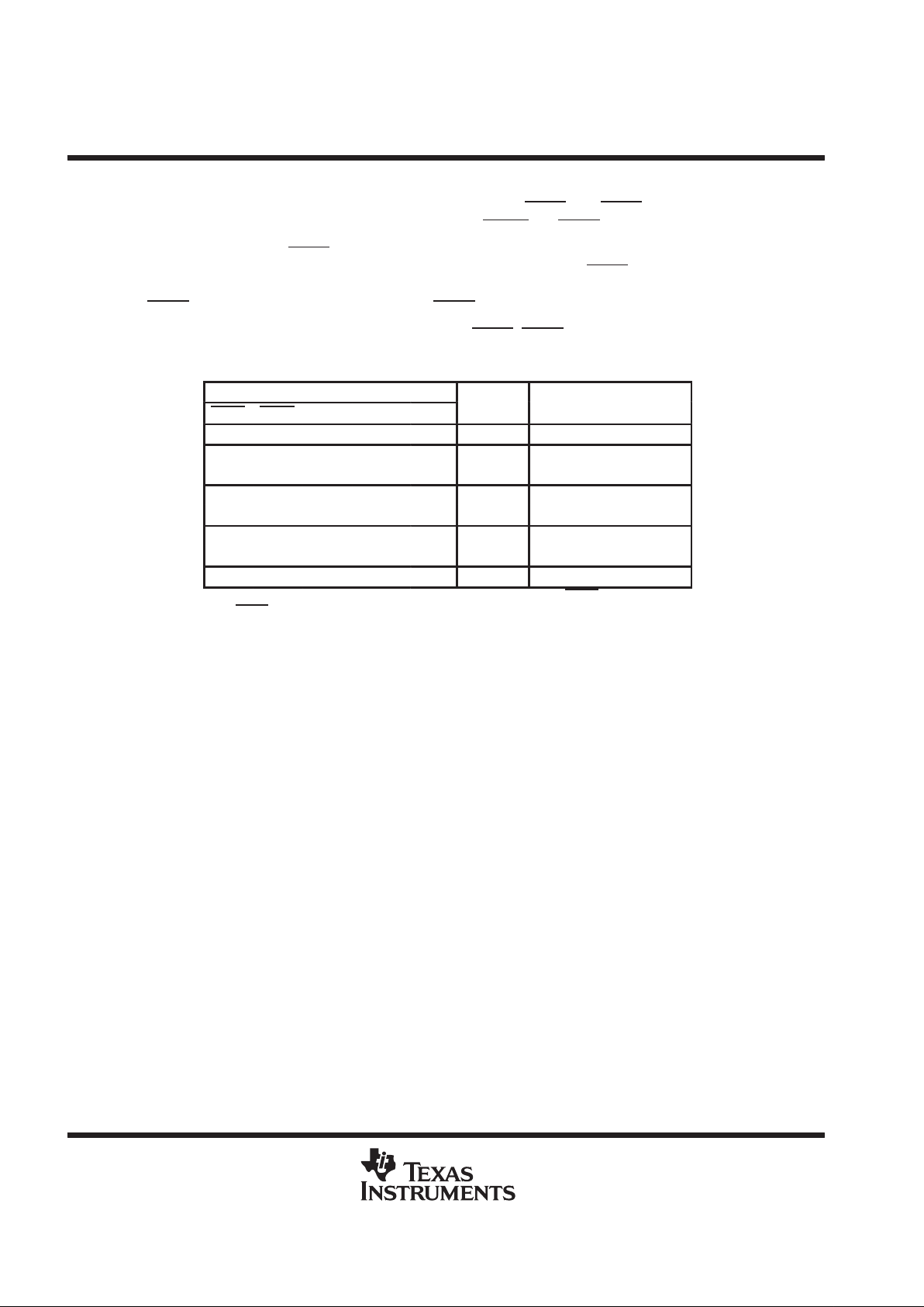
FUNCTION TABLE
†
INPUTS
OUTPUT
CEAB OEAB LEAB CLKAB A
B
MODE
X H X X X Z Isolation
L L L H or L X B
0
‡
L L L H or L X B
0
§
Latched storage of A data
X L H X L L
p
X LH XH H
Transparent
L L L ↑ L L
L LL ↑ HH
Clocked storage of A data
H L L X X B
0
§
Clock inhibit
†
A-to-B data flow is shown. B-to-A data flow is similar, but uses OEBA, LEBA, CLKBA,
and CEBA
.
‡
Output level before the indicated steady-state input conditions were established, provided
that CLKAB was high before LEAB went low.
§
Output level before the indicated steady-state input conditions were established.
 Loading...