

SN54GTL16622A, SN74GTL16622A
18-BIT LVTTL-TO-GTL/GTL+ BUS TRANSCEIVERS
SCBS673D – AUGUST 1996 – REVISED DECEMBER 1999
D
Members of the Texas Instruments
Widebus
D
D-Type Flip-Flops With Qualified Storage
Family
Enable
D
Translate Between GTL/GTL+ Signal Levels
and LVTTL Logic Levels
D
Support Mixed-Mode (3.3 V and 5 V) Signal
Operation on A-Port and Control Inputs
D
I
Supports Partial-Power-Down Mode
off
Operation
D
Bus Hold on Data Inputs Eliminates the
Need for External Pullup/Pulldown
Resistors on A Port
D
ESD Protection Exceeds JESD 22
– 2000-V Human-Body Model (A114-A)
– 200-V Machine Model (A115-A)
– 1000-V Charged-Device Model (C101)
D
Latch-Up Performance Exceeds 250 mA Per
JESD 17
D
Distributed VCC and GND-Pin Configuration
Minimizes High-Speed Noise
D
Package Options Include Plastic Thin
Shrink Small-Outline (DGG) and Ceramic
Quad Flat (HV) Packages
description
The ’GTL16622A devices are 18-bit
registered bus transceivers that provide
LVTTL-to-GTL/GTL+ and GTL/GTL+-to-LVTTL
signal-level translation. They are partitioned as
two separate 9-bit transceivers with individual
clock-enable controls and contain D-type
flip-flops for temporary storage of data flowing in
either direction. The devices provide an interface
between cards operating at LVTTL logic levels
and a backplane operating at GTL/GTL+ signal
levels. Higher speed operation is a direct result of
the reduced output swing (<1 V), reduced input
threshold levels, and output edge control
(OEC).
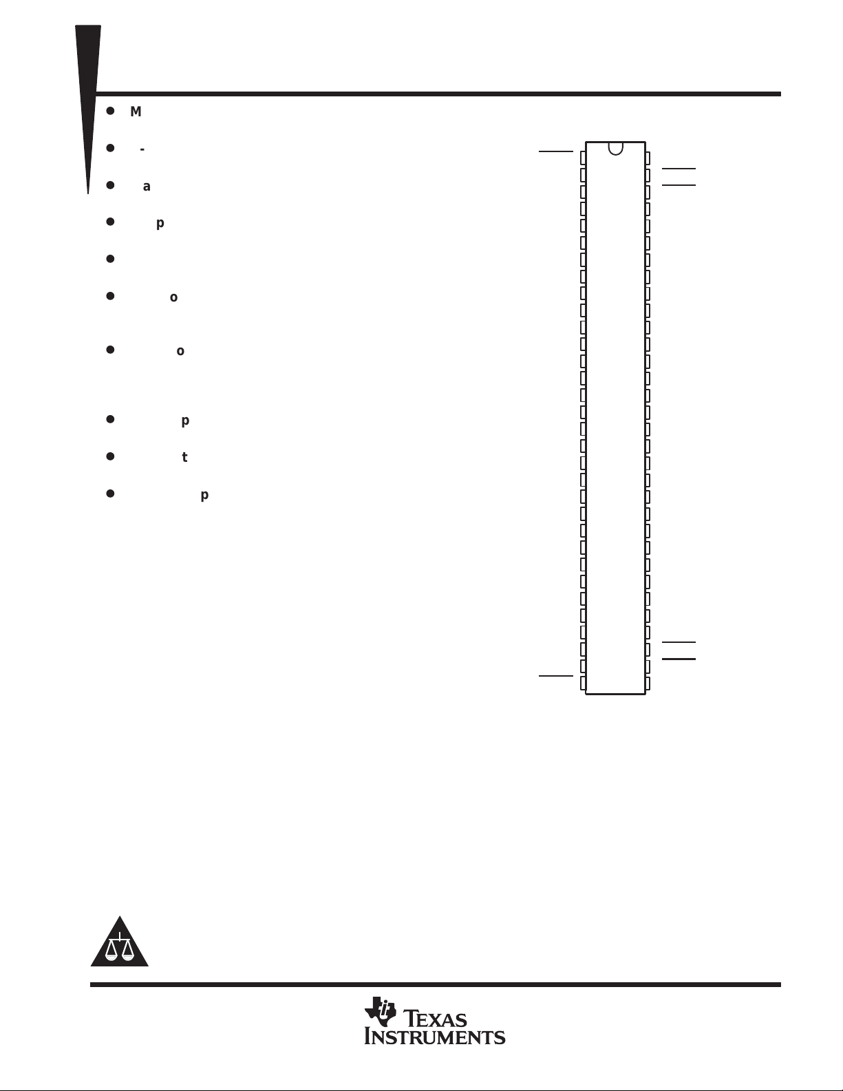
SN74GTL16622A . . . DGG PACKAGE
OEAB
OEBA
1A1
GND
1A2
1A3
GND
V
CC
1A4
GND
1A5
1A6
GND
1A7
1A8
GND
1A9
2A1
GND
2A2
2A3
GND
2A4
2A5
GND
2A6
V
CC
GND
2A7
2A8
GND
2A9
(TOP VIEW)
1
64
2
63
3
62
4
61
5
60
6
59
7
58
8
57
9
56
10
55
11
54
12
53
13
52
14
51
15
50
16
49
17
48
18
47
19
46
20
45
21
44
22
43
23
42
24
41
25
40
26
39
27
38
28
37
29
36
30
35
31
34
32
33
CLKAB
1CEAB
1CEBA
1B1
GND
1B2
1B3
V
CC
1B4
1B5
1B6
GND
1B7
1B8
GND
1B9
2B1
GND
2B2
2B3
GND
2B4
2B5
2B6
V
REF
2B7
2B8
GND
2B9
2CEBA
2CEAB
CLKBA
The user has the flexibility of using this device at either GTL (V
higher noise margin GTL+ (V
= 1.5 V and V
TT
= 1 V) signal levels. GTL+ is the T exas Instruments derivative
REF
= 1.2 V and V
TT
= 0.8 V) or the preferred
REF
of the Gunning transceiver logic (GTL) JEDEC standard JESD 8-3. The B port normally operates at GTL or
GTL+ signal levels, while the A-port and control inputs are compatible with LVTTL logic levels and are 5-V
tolerant. V
Please be aware that an important notice concerning availability, standard warranty, and use in critical applications of
Texas Instruments semiconductor products and disclaimers thereto appears at the end of this data sheet.
OEC and Widebus are trademarks of Texas Instruments Incorporated.
UNLESS OTHERWISE NOTED this document contains PRODUCTION
DATA information current as of publication date. Products conform to
specifications per the terms of Texas Instruments standard warranty.
Production processing does not necessarily include testing of all
parameters.
is the reference input voltage for the B port.
REF
POST OFFICE BOX 655303 • DALLAS, TEXAS 75265
Copyright 1999, Texas Instruments Incorporated
1
SN54GTL16622A, SN74GTL16622A
18-BIT LVTTL-TO-GTL/GTL+ BUS TRANSCEIVERS
SCBS673D – AUGUST 1996 – REVISED DECEMBER 1999
description (continued)
Data flow in each direction is controlled by the output-enable (OEAB and OEBA) and clock (CLKAB and CLKBA)
inputs. The clock-enable (CEAB and CEBA) inputs are designed to control each 9-bit transceiver independently ,
which makes the device more versatile.
For A-to-B data flow, the device operates on the low-to-high transition of CLKAB if CEAB is low. When OEAB
is low, the outputs are active. When OEAB is high, the outputs are in the high-impedance state. Data flow for
B to A is similar to that of A to B, but uses OEBA, CLKBA, and CEBA.
These devices are fully specified for partial-power-down applications using I
. The I
off
circuitry disables the
off
outputs, preventing damaging current backflow through the device when it is powered down.
Active bus-hold circuitry holds unused or undriven L VTTL inputs at a valid logic state. Use of pullup or pulldown
resistors with the bus-hold circuitry is not recommended.
T o ensure the high-impedance state during power up or power down, OE should be tied to VCC through a pullup
resistor; the minimum value of the resistor is determined by the current-sinking capability of the driver.
The SN54GTL16622A is characterized for operation over the full military temperature range of –55°C to 125°C.
The SN74GTL16622A is characterized for operation from –40°C to 85°C.
GND
1A5
1A6
GND
1A7
1A8
GND
1A9
NC
2A1
GND
2A2
2A3
GND
2A4
2A5
GND
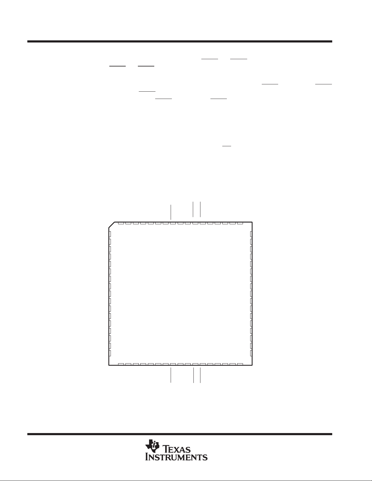
SN54GTL16622A . . . HV PACKAGE
CC
1A4
GND
1A3
V
9876543216867666564636261
10
11
12
13
14
15
16
17
18
19
20
21
22
23
24
25
26
27 28 29 30 31 32 33 34 35 36 37 38 39 40 41 42 43
1A2
GND
(TOP VIEW)
NC
OEAB
1A1
CLKAB
1CEAB
1CEBA
1B1
GND
1B2
1B3
CC
V
1B4
60
1B5
59
1B6
58
GND
57
1B7
56
1B8
55
GND
54
1B9
53
NC
52
2B1
51
GND
50
2B2
49
2B3
48
GND
47
2B4
46
2B5
45
2B6
44
CC
2A6
NC – No internal connection
2
2A7
GND
2A8
GND
V
POST OFFICE BOX 655303 • DALLAS, TEXAS 75265
2A9
NC
OEBA
2CEAB
CLKBA
2B9
2CEBA
GND
2B8
2B7
REF
V
MODE
Latched storage of A data
Clocked storage of A data
SN54GTL16622A, SN74GTL16622A
18-BIT LVTTL-TO-GTL/GTL+ BUS TRANSCEIVERS
SCBS673D – AUGUST 1996 – REVISED DECEMBER 1999
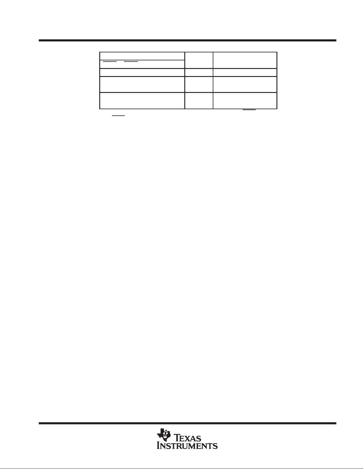
FUNCTION TABLE
INPUTS
CEAB OEAB CLKAB A
X H X X Z Isolation
H L X X B
X L H or L X B
L L ↑ L L
L L ↑ H H
†
A-to-B data flow is shown. B-to-A data flow is similar, but uses OEBA, CLKBA,
and CEBA
‡
Output level before the indicated steady-state input conditions are established
.
OUTPUT
†
B
‡
0
‡
0
POST OFFICE BOX 655303 • DALLAS, TEXAS 75265
3
 Loading...