

Datasheet SN74GTL16612ADGGR, SN74GTL16612ADL, SN74GTL16612ADLR Datasheet (Texas Instruments)
SN54GTL16612A, SN74GTL16612A
18-BIT LVTTL-TO-GTL+ UNIVERSAL BUS TRANSCEIVERS
SCES187D – JANUARY 1999 – REVISED DECEMBER 1999
D
Members of the Texas Instruments
Widebus
D
Universal Bus Transceiver (
Family
UBT
)
Combines D-Type Latches and D-Type
Flip-Flops for Operation in Transparent,
Latched, Clocked, or Clock-Enabled Mode
D
Translate Between GTL/GTL+ Signal Levels
and LVTTL Logic Levels
D
Support Mixed-Mode (3.3-V and 5-V) Signal
Operation on A-Port and Control Inputs
D
B-Port Transition T ime Optimized for
Distributed Backplane Loads
D
I
Supports Partial-Power-Down Mode
off
Operation
description
The ’GTL16612A devices are 18-bit universal bus transceivers (UBT) that provide LVTTL-to-GTL+ and
GTL+-to-L VTTL signal-level translation. They allow for transparent, latched, clocked, or clock-enabled modes
of data transfer. These devices provide a high-speed interface between cards operating at LVTTL logic levels
and backplanes operating at GTL+ signal levels. High-speed (about two times faster than standard L VTTL or
TTL) backplane operation is a direct result of the reduced output swing (<1 V), reduced input threshold levels,
and output edge control (OEC). Improved GTL+ OEC circuits minimize bus settling time and have been
designed and tested using several backplane models.
D
Bus Hold on A-Port Inputs Eliminates the
Need for External Pullup/Pulldown
Resistors
D
Distributed VCC and GND-Pin Configuration
Minimizes High-Speed Switching Noise
D
ESD Protection Exceeds JESD 22
– 2000-V Human-Body Model (A114-A)
– 200-V Machine Model (A115-A)
– 1000-V Charged-Device Model (C101)
D
Latch-Up Performance Exceeds 100 mA Per
JESD 78, Class II
D
Package Options Include Plastic Shrink
Small-Outline (DL), Thin Shrink
Small-Outline (DGG), and Ceramic Flat
(WD) Packages
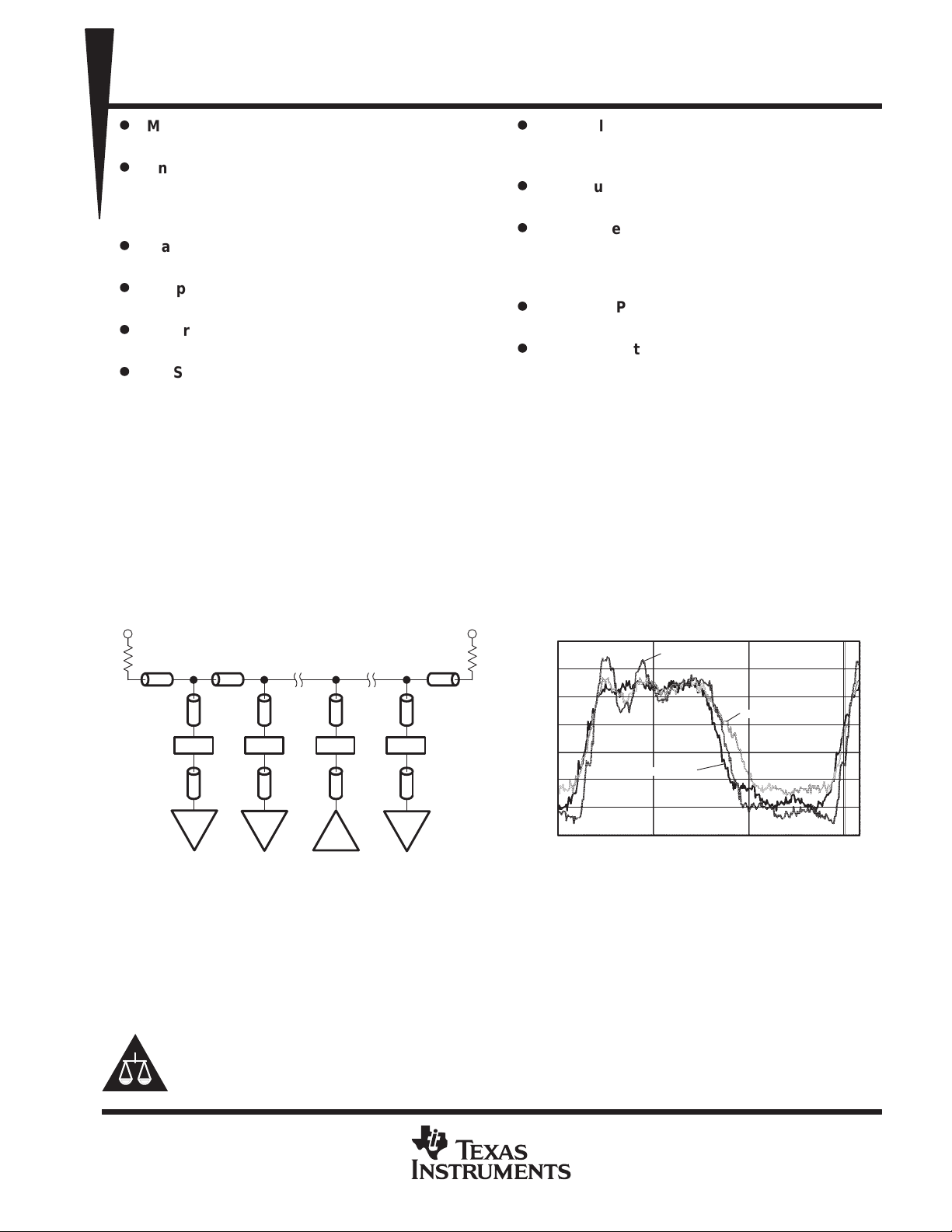
V
TT
.25”
TT
R
V
TT
.875”
.625” .625”
Conn.
1” 1”
Rcvr
Slot 1 Slot 2
.625”.625”
Conn. Conn. Conn.
1”1”
Rcvr
Drvr
Slot 8
Rcvr
Slot 16
.25”
R
TT
1.8
1.6
1.4
1.2
1.0
Volts – V
0.8
0.6
0.4
020
TI GTL16612
Fairchild GTLP16612
TI GTL16612A
10 30
t – Time – ns
Figure 1. Test Backplane Model With Output Waveform Results
Please be aware that an important notice concerning availability, standard warranty, and use in critical applications of
Texas Instruments semiconductor products and disclaimers thereto appears at the end of this data sheet.
TI, OEC, UBT, and Widebus are trademarks of Texas Instruments Incorporated.
UNLESS OTHERWISE NOTED this document contains PRODUCTION
DATA information current as of publication date. Products conform to
specifications per the terms of Texas Instruments standard warranty.
Production processing does not necessarily include testing of all
parameters.
POST OFFICE BOX 655303 • DALLAS, TEXAS 75265
Copyright 1999, Texas Instruments Incorporated
1
SN54GTL16612A, SN74GTL16612A
18-BIT LVTTL-TO-GTL+ UNIVERSAL BUS TRANSCEIVERS
SCES187D – JANUARY 1999 – REVISED DECEMBER 1999
description (continued)
Figure 1 shows actual device output waveforms using a synchronous clock at 75 MHz. The test backplane is
a 16-slot, 14-inch board with loaded impedance of 33 Ω. VTT is 1.5 V , V
The driver is in slot 8, with receivers in alternate slots 1, 3, 5, 7, 10, 12, 14, and 16. Receiver slot 1 signals are
shown. The signal becomes progressively worse as the receiver moves closer to the driver or the spacing
between receiver cards is reduced. The clock is independent of the data and the system clock frequency is
limited by the backplane flight time to about 80–90 MHz. This frequency can be increased even more (30% to
40%) if the clock is generated and transmitted together with the data off the driver card (source synchronous).
is 1 V , and RTT pullup resistor is 50 Ω.
REF
Additional design considerations can be found in
Application Information
at the end of this data sheet.
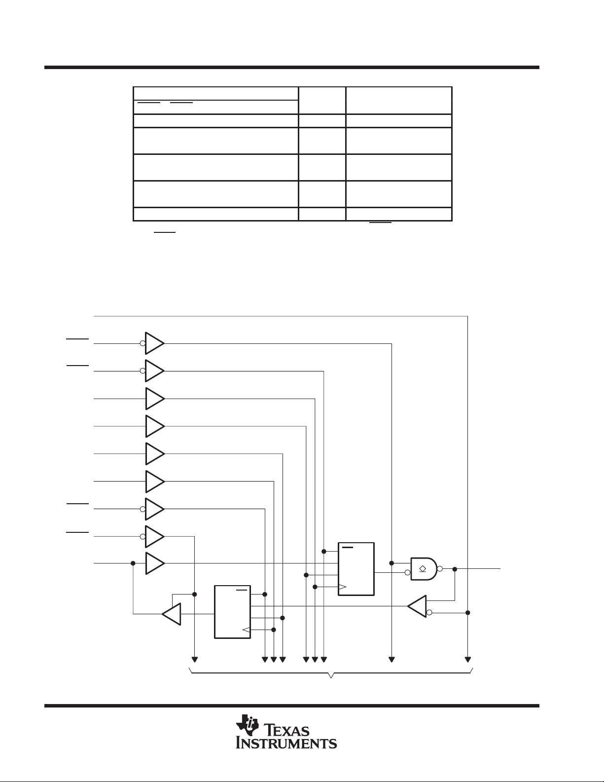
These 18-bit universal bus transceivers combine D-type latches and D-type flip-flops to allow data flow in
transparent, latched, clocked, and clock-enabled modes. These UBTs can replace any of the functions shown
in Table 1.
Table 1. ’GTL16612A UBT Replacement Functions
FUNCTION 8 BIT 9 BIT 10 BIT 16 BIT 18 BIT
Transceiver ’245, ’623, ’645 ’863 ’861 ’16245, ’16623 ’16863
Buffer/driver ’241, ’244, ’541 ’827 ’16241, ’16244, ’16541 ’16825
Latched transceiver ’543 ’16543 ’16472
Latch ’373, ’573 ’843 ’841 ’16373 ’16843
Registered transceiver ’646, ’652 ’16646, ’16652 ’16474
Flip-flop ’374, ’574 ’821 ’16374
Standard UBT ’16500, ’16501
Universal bus driver ’16835
Registered transceiver with CLK enable ’2952 ’16470, ’16952
Flip-flop with CLK enable ’377 ’823 ’16823
Standard UBT with CLK enable ’16600, ’16601
’GTL16612A UBT replaces all above functions
GTL+ is the Texas Instruments (TI) derivative of the Gunning transceiver logic (GTL) JEDEC standard
JESD 8-3. The AC specification of the ’GTL16612A is given only at the preferred higher noise margin GTL+,
but this device can be used at either GTL (V
= 1.2 V and V
TT
= 0.8 V) or GTL+ (V
REF
= 1.5 V and V
TT
REF
= 1 V)
signal levels.
The B port normally operates at GTL or GTL+ levels, while the A-port and control inputs are compatible with
LVTTL logic levels and are 5-V tolerant. V
is the reference input voltage for the B port.
REF
T o improve signal integrity , the ’GTL16612A B-port output transition time is optimized for distributed backplane
loads.
(5 V) supplies the internal and GTL circuitry, while VCC (3.3 V) supplies the LVTTL output buffers.
V
CC
Data flow in each direction is controlled by output-enable (OEAB and OEBA), latch-enable (LEAB and LEBA),
and clock (CLKAB and CLKBA) inputs. The clock or latch enable can be controlled by the clock-enable (CEAB
and CEBA) inputs. For A-to-B data flow, the devices operate in the transparent mode when LEAB is high. When
LEAB is low , the A data is latched if CEAB
is low and CLKAB is held at a high or low logic level. If LEAB is low,
the A data is stored in the latch/flip-flop on the low-to-high transition of CLKAB if CEAB also is low. When OEAB
is low, the outputs are active. When OEAB is high, the outputs are in the high-impedance state. Data flow for
B to A is similar to that for A to B, but uses OEBA, LEBA, CLKBA, and CEBA.
T o ensure the high-impedance state during power up or power down, OE should be tied to VCC through a pullup
resistor; the minimum value of the resistor is determined by the current-sinking capability of the driver.
2
POST OFFICE BOX 655303 • DALLAS, TEXAS 75265
SN54GTL16612A, SN74GTL16612A
18-BIT LVTTL-TO-GTL+ UNIVERSAL BUS TRANSCEIVERS
SCES187D – JANUARY 1999 – REVISED DECEMBER 1999
description (continued)
Active bus-hold circuitry holds unused or undriven L VTTL inputs at a valid logic state. Use of pullup or pulldown
resistors with the bus-hold circuitry is not recommended.
These devices are fully specified for partial-power-down applications using I
. The I
off
circuitry disables the
off
outputs, preventing damaging current backflow through the devices when they are powered down.
The SN54GTL16612A is characterized for operation over the full military temperature range of –55°C to 125°C.
The SN74GTL16612A is characterized for operation from –40°C to 85°C.
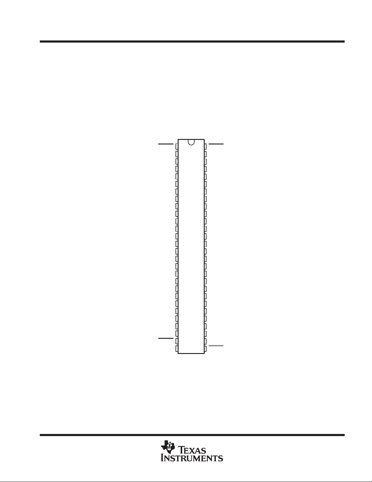
SN54GTL16612A ...WD PACKAGE
SN74GTL16612A . . . DGG OR DL PACKAGE
OEAB
LEAB
V
(3.3 V)
CC
V
(3.3 V)
CC
OEBA
LEBA
A1
GND
A2
A3
A4
A5
A6
GND
A7
A8
A9
A10
A11
A12
GND
A13
A14
A15
A16
A17
GND
A18
(TOP VIEW)
1
56
2
55
3
54
4
53
5
52
6
51
7
50
8
49
9
48
10
47
11
46
12
45
13
44
14
43
15
42
16
41
17
40
18
39
19
38
20
37
21
36
22
35
23
34
24
33
25
32
26
31
27
30
28
29
CEAB
CLKAB
B1
GND
B2
B3
V
(5 V)
CC
B4
B5
B6
GND
B7
B8
B9
B10
B11
B12
GND
B13
B14
B15
V
REF
B16
B17
GND
B18
CLKBA
CEBA
POST OFFICE BOX 655303 • DALLAS, TEXAS 75265
3
SN54GTL16612A, SN74GTL16612A
MODE
Latched storage of A data
Transparent
Clocked storage of A data
18-BIT LVTTL-TO-GTL+ UNIVERSAL BUS TRANSCEIVERS
SCES187D – JANUARY 1999 – REVISED DECEMBER 1999
CEAB OEAB LEAB CLKAB A
X H X X X Z Isolation
L L L H X B
L LL LXB
X L H X L L
X LH XH H
L L L ↑ L L
L LL ↑ HH
H L L X X B
†
A-to-B data flow is shown. B-to-A data flow is similar, but uses OEBA, LEBA, CLKBA,
and CEBA
‡
Output level before the indicated steady-state input conditions were established, provided
that CLKAB was high before LEAB went low
§
Output level before the indicated steady-state input conditions were established
.
logic diagram (positive logic)
V
OEAB
CEAB
35
REF
1
56
INPUTS
FUNCTION TABLE
OUTPUT
†
B
‡
0
§
0
p
§
0
Clock inhibit
CLKAB
LEAB
LEBA
CLKBA
CEBA
OEBA
A1
55
2
28
30
29
27
3
CLK
CE
1D
C1
CE
1D
C1
CLK
54
B1
4
To 17 Other Channels
POST OFFICE BOX 655303 • DALLAS, TEXAS 75265

UNIT
VCCSuppl
oltage
V
VTTTermination voltage
V
V
Suppl
oltage
V
VIInput voltage
V
V
g
V
V
V
I
mA
SN54GTL16612A, SN74GTL16612A
18-BIT LVTTL-TO-GTL+ UNIVERSAL BUS TRANSCEIVERS
SCES187D – JANUARY 1999 – REVISED DECEMBER 1999
absolute maximum ratings over operating free-air temperature range (unless otherwise noted)
Supply voltage range, VCC: 3.3 V –0.5 V to 4.6 V. . . . . . . . . . . . . . . . . . . . . . . . . . . . . . . . . . . . . . . . . . . . . . . . . . .
5 V –0.5 V to 7 V. . . . . . . . . . . . . . . . . . . . . . . . . . . . . . . . . . . . . . . . . . . . . . . . . . . . .
Input voltage range, V
Voltage range applied to any output in the high or power-off state, V
(see Note 1): A port –0.5 V to 7 V. . . . . . . . . . . . . . . . . . . . . . . . . . . . . . . . . . . . . . . . . . . . . . . . . . . . . . . . . . . . .
Current into any output in the low state, I
Current into any A-port output in the high state, I
Continuous current through each VCC or GND ±100 mA. . . . . . . . . . . . . . . . . . . . . . . . . . . . . . . . . . . . . . . . . . . . .
Input clamp current, I
Output clamp current, I
Package thermal impedance, θJA (see Note 3): DGG package 64°C/W. . . . . . . . . . . . . . . . . . . . . . . . . . . . . . .
Storage temperature range, T
†
Stresses beyond those listed under “absolute maximum ratings” may cause permanent damage to the device. These are stress ratings only, and
functional operation of the device at these or any other conditions beyond those indicated under “recommended operating conditions” is not
implied. Exposure to absolute-maximum-rated conditions for extended periods may affect device reliability.
NOTES: 1. The input and output negative-voltage ratings may be exceeded if the input and output clamp-current ratings are observed.
2. This current flows only when the output is in the high state and VO > VCC.
3. The package thermal impedance is calculated in accordance with JESD 51.
(see Note 1): A-port and control inputs –0.5 V to 7 V. . . . . . . . . . . . . . . . . . . . . . . . . . .
I
B port and V
–0.5 V to 4.6 V. . . . . . . . . . . . . . . . . . . . . . . . . . . . . . . . .
REF
O
B port –0.5 V to 4.6 V. . . . . . . . . . . . . . . . . . . . . . . . . . . . . . . . . . . . . . . . . . . . . . . . . . . . . . . . . . . .
: A port 128 mA. . . . . . . . . . . . . . . . . . . . . . . . . . . . . . . . . . . . . . . . . . .
O
B port 80 mA. . . . . . . . . . . . . . . . . . . . . . . . . . . . . . . . . . . . . . . . . . . .
(see Note 2) 64 mA. . . . . . . . . . . . . . . . . . . . . . . . . . . . . . . .
O
(V
< 0) –50 mA. . . . . . . . . . . . . . . . . . . . . . . . . . . . . . . . . . . . . . . . . . . . . . . . . . . . . . . . . . .
IK
I
(V
OK
< 0) –50 mA. . . . . . . . . . . . . . . . . . . . . . . . . . . . . . . . . . . . . . . . . . . . . . . . . . . . . . . .
O
DL package 56°C/W. . . . . . . . . . . . . . . . . . . . . . . . . . . . . . . . .
–65°C to 150°C. . . . . . . . . . . . . . . . . . . . . . . . . . . . . . . . . . . . . . . . . . . . . . . . . . .
stg
†
recommended operating conditions (see Notes 4 through 6)
SN54GTL16612A SN74GTL16612A
MIN NOM MAX MIN NOM MAX
pp
y v
pp
REF
IH
IL
I
IK
I
OH
OL
T
A
NOTES: 4. All unused control inputs of the device must be held at VCC or GND to ensure proper device operation. Refer to the TI application
y v
p
High-level
input voltage
Low-level
input voltage
Input clamp current –18 –18 mA
High-level
output current
Low-level
output current
Operating free-air temperature –55 125 –40 85 °C
report
5. Normal connection sequence is GND first, VCC = 5 V second, and VCC = 3.3 V , I/O, control inputs, VTT, and V
6. VTT and RTT can be adjusted to accommodate backplane impedances as long as they do not exceed the DC absolute IOL ratings.
Implications of Slow or Floating CMOS Inputs
Similarly , V
3.3 V 3.15 3.3 3.45 3.15 3.3 3.45
5 V 4.75 5 5.25 4.75 5 5.25
GTL 1.14 1.2 1.26 1.14 1.2 1.26
GTL+ 1.35 1.5 1.65 1.35 1.5 1.65
GTL 0.74 0.8 0.87 0.74 0.8 0.87
GTL+ 0.87 1 1.1 0.87 1 1.1
B port V
Except B port 5.5 5.5
B port V
Except B port
B port V
Except B port
A port –32 –32 mA
A port 64 64
B port
can be adjusted to optimize noise margins, but normally is 2/3 VTT.
REF
+50 mV V
REF
2 2
, literature number SCBA004.
TT
+50 mV
REF
–50 mV V
REF
0.8 0.8
34 34
REF
V
TT
–50 mV
(any order) last.
REF
PRODUCT PREVIEW information concerns products in the formative or
design phase of development. Characteristic data and other
specifications are design goals. Texas Instruments reserves the right to
change or discontinue these products without notice.
POST OFFICE BOX 655303 • DALLAS, TEXAS 75265
5

SN54GTL16612A, SN74GTL16612A
PARAMETER
TEST CONDITIONS
UNIT
CC
() ,
A port
CC
() ,
I
V
CC
V
µ
B port
CC
() ,
()
V
CC
V
µ
OZH
µ
I
A
§
(3.3V)
ort
V
I
V
CC
GND
§
§
(5 V)
ort
V
I
V
CC
GND
§
C
pF
18-BIT LVTTL-TO-GTL+ UNIVERSAL BUS TRANSCEIVERS
SCES187D – JANUARY 1999 – REVISED DECEMBER 1999
electrical characteristics over recommended operating free-air temperature range (unless
otherwise noted)
SN54GTL16612A SN74GTL16612A
MIN TYP†MAX MIN TYP†MAX
V
IK
V
V
I
I
off
I
I(hold)
I
OZL
I
CC
I
CC
∆ICC (3.3 V)
C
†
All typical values are at VCC (3.3 V) = 3.3 V, VCC (5 V) = 5 V, TA = 25°C.
‡
This is the bus-hold maximum dynamic current. It is the minimum overdrive current required to switch the input from one state to another.
§
This is the VI for A-port or control inputs.
¶
This is the VI for B port.
#
This is the increase in supply current for each input that is at the specified TTL voltage level rather than VCC or GND.
A port
OH
OL
B port VCC (3.3 V) = 3.15 V, VCC (5 V) = 4.75 V, IOL = 34 mA 0.65 0.65
Control
inputs
A port
A port
A port
B port VCC (3.3 V) = 3.45 V, VCC (5 V) = 5.25 V, VO = 1.5 V 10 10
A port VCC (3.3 V) = 3.45 V, VCC (5 V) = 5.25 V, VO = 0 –1 –1
B port VCC (3.3 V) = 3.45 V, VCC (5 V) = 5.25 V, VO = 0.65 V –10 –10
A or B
p
A or B
p
Control
i
inputs
A port VO = 3.15 V or 0 8.5 18 8.5
io
B port VO = 1.5 V or 0 10 8
VCC (3.3 V) = 3.15 V,
VCC (5 V) = 4.75 V
VCC (3.3 V) = 3.15 V to 3.45 V,
VCC (5 V) = 4.75 V to 5.25 V
V
(3.3 V) = 3.15 V,
VCC (5 V) = 4.75 V
V
p
p
#
(3.3 V) = 3.15 V,
VCC (5 V) = 4.75 V
VCC (3.3 V) = 0 or 3.45 V,
VCC (5 V) = 0 or 5.25 V
VCC (3.3 V) = 3.45 V,
(5 V) = 5.25
V
(3.3 V) = 3.45 V,
VCC (5 V) = 5.25 V
VCC = 0, VI or VO = 0 to 4.5 V 1000 100 µA
VCC (3.3 V) = 3.15 V,
(5 V) = 4.75
VCC (3.3 V) = 3.45 V,
VCC (5 V) = 5.25 V
VCC (3.3 V) = 3.45 V,
VCC (5 V) = 5.25 V, IO = 0,
=
=
(3.3 V) or
VI = VTT or GND
VCC (3.3 V) = 3.45 V,
VCC (5 V) = 5.25 V, IO = 0,
=
=
VI = VTT or GND
VCC (3.3 V) = 3.45 V, VCC (5 V) = 5.25 V,
One A-port or control input at 2.7 V ,
Other A-port or control inputs at VCC (3.3 V) or GND
VI = 3.15 V or 0 4 12 4 pF
¶
(3.3 V) or
¶
II = –18 mA –1.2 –1.2 V
IOH = –100 µA VCC (3.3 V)–0.2 VCC (3.3 V)–0.2
IOH = –8 mA 2.4 2.4
IOH = –32 mA 2 2
IOL = 100 µA 0.2 0.2
IOL = 16 mA 0.4 0.4
IOL = 32 mA 0.5 0.5
IOL = 64 mA 0.6 0.55
VI = 5.5 V 10 10
VI = 5.5 V 1000 20
VI = VCC (3.3 V) 1 1
VI = 0 –30 –30
VI = VCC (3.3 V) 5 5
VI = 0 –5 –5
VI = 0.8 V 75 75
VI = 2 V –75 –75
VI = 0 to VCC(3.3 V)
VO = VCC (3.3 V) 1 1
Outputs high 1 1
Outputs low 5 5
,
Outputs disabled 1 1
Outputs high 120 120
Outputs low 120 120
,
Outputs disabled 120 120
‡
±500 ±500
1 1 mA
V
V
µA
µA
A
µ
mA
mA
p
PRODUCT PREVIEW information concerns products in the formative or
design phase of development. Characteristic data and other
specifications are design goals. Texas Instruments reserves the right to
change or discontinue these products without notice.
6
POST OFFICE BOX 655303 • DALLAS, TEXAS 75265

UNIT
twPulse duration
ns
tsuSetup time
ns
thHold time
ns
PARAMETER
UNIT
A
B
ns
LEAB
B
ns
CLKAB
B
ns
OEAB
B
ns
B
A
ns
LEBA
A
ns
CLKBA
A
ns
OEBA
A
ns
SN54GTL16612A, SN74GTL16612A
18-BIT LVTTL-TO-GTL+ UNIVERSAL BUS TRANSCEIVERS
SCES187D – JANUARY 1999 – REVISED DECEMBER 1999
timing requirements over recommended ranges of supply voltage and operating free-air
temperature, V
f
clock
Clock frequency 85 85 MHz
p
= 1.5 V and V
TT
= 1 V for GTL+ (unless otherwise noted) (see Figure 2)
REF
SN54GTL16612A SN74GTL16612A
MIN MAX MIN MAX
LEAB or LEBA high 3.3 3.3
CLKAB or CLKBA high or low 5.7 5.7
A before CLKAB↑ 1 1
B before CLKBA↑ 2.7 1.8
A before LEAB↓ 1.7 0.5
B before LEBA↓ 1.2 1.2
CEAB before CLKAB↑ 1.3 1.2
CEBA before CLKBA↑ 1.8 1.4
A after CLKAB↑ 3.2 1.9
B after CLKBA↑ 4.3 0.5
A after LEAB↓ 3.2 2.7
B after LEBA↓ 4.2 3.5
CEAB after CLKAB↑ 2.4 1.2
CEBA after CLKBA↑ 1.1 1.1
switching characteristics over recommended ranges of supply voltage and operating free-air
temperature, V
f
max
t
PLH
t
PHL
t
PLH
t
PHL
t
PLH
t
PHL
t
en
t
dis
t
r
t
f
t
PLH
t
PHL
t
PLH
t
PHL
t
PLH
t
PHL
t
en
t
†
All typical values are at VCC (3.3 V) = 3.3 V, VCC (5 V) = 5 V, TA = 25°C.
dis
= 1.5 V and V
TT
Transition time, B outputs (20% to 80%) 2.6 2.6 ns
Transition time, B outputs (80% to 20%) 2.6 2.6 ns
FROM TO
(INPUT) (OUTPUT)
= 1 V for GTL+ (see Figure 2)
REF
SN54GTL16612A SN74GTL16612A
MIN TYP†MAX MIN TYP†MAX
85 85 MHz
2 7.3 2.5 6.9
2.2 7.4 2.5 6.9
2.2 7.5 3.2 7.3
2.3 7.9 3.2 7.3
2.1 8 3.4 7.8
2.5 7.9 3.4 7.8
1.8 7.4 2.8 7
1.8 7 2.8 7
1.4 6.3 1.5 5.7
1.3 6.2 1.5 5.7
1.5 6.1 1.8 5.7
1 6 1.8 5.7
1.8 5.8 2.3 5.5
2 5.9 2.3 5.5
0.5 6.2 1.8 6.1
1.3 6.6 1.8 6.1
PRODUCT PREVIEW information concerns products in the formative or
design phase of development. Characteristic data and other
specifications are design goals. Texas Instruments reserves the right to
change or discontinue these products without notice.
POST OFFICE BOX 655303 • DALLAS, TEXAS 75265
7

SN54GTL16612A, SN74GTL16612A
18-BIT LVTTL-TO-GTL+ UNIVERSAL BUS TRANSCEIVERS
SCES187D – JANUARY 1999 – REVISED DECEMBER 1999
PARAMETER MEASUREMENT INFORMATION
From Output
Under Test
CL = 50 pF
(see Note A)
LOAD CIRCUIT FOR A OUTPUTS
Input
Input
t
PLH
Output
Input
t
PLH
Output
500 Ω
500 Ω
t
w
1.5 V
VOLTAGE WAVEFORMS
PULSE DURATION
1.5 V 1.5 V
V
REF
VOLTAGE WAVEFORMS
PROPAGATION DELAY TIMES
(A port to B port)
V
REF
1.5 V 1.5 V
VOLTAGE WAVEFORMS
PROPAGATION DELAY TIMES
(B port to A port)
S1
V
1.5 V
REF
6 V
Open
GND
t
V
REF
PHL
t
PHL
3 V
0 V
3 V
0 V
V
V
V
0 V
V
V
TT
OL
TT
OH
OL
TEST
t
PLH/tPHL
t
PLZ/tPZL
t
PHZ/tPZH
Waveform 1
(see Note B)
Waveform 2
S1 at GND
(see Note B)
Timing
Input
Data Input
A Port
Data Input
B Port
Output
Control
Output
S1 at 6 V
Output
S1
Open
6 V
GND
VOLTAGE WAVEFORMS
SETUP AND HOLD TIMES
t
PZL
t
PZH
VOLTAGE WAVEFORMS
ENABLE AND DISABLE TIMES
From Output
Under Test
LOAD CIRCUIT FOR B OUTPUTS
t
su
1.5 V
V
REF
1.5 V 1.5 V
1.5 V
1.5 V
(A port)
CL = 30 pF
(see Note A)
1.5 V
t
h
VOL + 0.3 V
VOH – 0.3 V
V
1.5 V
V
REF
t
PLZ
t
PHZ
TT
25 Ω
Test
Point
3 V
0 V
3 V
0 V
V
TT
0 V
3 V
0 V
3 V
V
OL
V
OH
≈0 V
NOTES: A. CL includes probe and jig capacitance.
B. Waveform 1 is for an output with internal conditions such that the output is low except when disabled by the output control.
Waveform 2 is for an output with internal conditions such that the output is high except when disabled by the output control.
C. All input pulses are supplied by generators having the following characteristics: PRR ≤ 10 MHz, ZO = 50 Ω, tr ≤ 2.5 ns, tf≤ 2.5 ns.
D. The outputs are measured one at a time with one transition per measurement.
Figure 2. Load Circuits and Voltage Waveforms
8
POST OFFICE BOX 655303 • DALLAS, TEXAS 75265

SN54GTL16612A, SN74GTL16612A
18-BIT LVTTL-TO-GTL+ UNIVERSAL BUS TRANSCEIVERS
SCES187D – JANUARY 1999 – REVISED DECEMBER 1999
APPLICATION INFORMATION
GTL background information
GTL was approved as JEDEC standard JESD 8-3 in 1993 and originally was created as a reduced-swing I/O
driver technology to support high-speed buses and backplanes. The GTL bus is designed to work with low
voltage swings. The input buffer works like an analog comparator rather than like an inverter , which allows the
GTL inputs to switch quickly without needing to be driven rail to rail. GTL drivers were designed to pull a 1.2-V
signal down to 0.4 V when switched on. This, however, placed the reference voltage for the input comparator
at 0.8 V, which made it susceptible to ground-bounce noise. A variant of GTL, called GTL+, is being used to
address this noise-margin concern. The GTL+ termination voltage is raised to 1.5 V , with the driver pulling down
to a V
TI GTL devices operate at, and are specified for, both GTL and the improved-noise-margin GTL+ standard.
However, the ’GTL16612A devices deviate from this history. They are designed with slow rising and falling
edges, to offer significant system frequency improvement in heavily loaded backplanes. They are AC specified
only at GTL+ because most applications are moving to this improved-noise-margin standard; they operate at
either GTL or GTL+.
Devices named GTL or GTLP indicate reduced voltage-swing operation at a VTT of 1.2 V (GTL standard) or
1.5 V (improved-noise-margin GTL+ standard). Fast-edge GTL devices are best for point-to-point or
lower-frequency backplanes. Slow-edge GTL devices extend backplane operations to cover even higher
frequencies.
of 0.5 V. This moved the reference voltage to 1 V and out of the range of most ground bounces.
OL
input characteristics
The input characteristics are identical on both A and B ports. Both ports are very high impedance and have an
input diode to provide protection against high negative-voltage spikes. The input diode conducts and prevents
more sensitive components from being destroyed as the result of electrostatic discharges or line reflections.
GTL output characteristics
The principle of the GTL bus is based on open-drain drivers, as shown in Figure 3.
TT
To Other Inputs InputOutput
R
TT
GTL Bus
V
TT
R
TT
needs to be greater than 25 Ω at GTL+ signal
TT
V
Figure 3. GTL Bus: An Open-Drain Bus
The devices actively drive the bus low, whereas, the termination voltage source, VTT pulls it high. Only the pullup
resistor (RTT), which usually is of a low resistance, limits the current. The pullup resistor value should match
the fully loaded backplane impedance, not the trace impedance, to provide an optimum termination of the bus
and avoid line reflections. The resistance of the GTL output is in the range of a few ohms. However, in the high
state, the output transistor is in the high-impedance state. R
levels, not to exceed the ’GTL16612A absolute maximum output current of 80 mA, and should be greater than
50 Ω at GTL+ signal levels, not to exceed the recommended output current limit of 34 mA.
POST OFFICE BOX 655303 • DALLAS, TEXAS 75265
9

SN54GTL16612A, SN74GTL16612A
18-BIT LVTTL-TO-GTL+ UNIVERSAL BUS TRANSCEIVERS
SCES187D – JANUARY 1999 – REVISED DECEMBER 1999
APPLICATION INFORMATION
OEC
The ’GTL16612A GTL output consists of an improved edge-control circuit that provides optimized rise and fall
times, typically 2.6 ns (20% to 80%), for backplanes under various loading conditions.
Using the definition of slew rate ∆t/∆v = tr or tf/(VOH – VOL), the slew rate of the device typically is 5 ns/V . As a
comparison, these values are significantly more than those of previous GTL or standard TTL devices, which
are usually about 1 ns/V, or less.
termination voltage, V
TT
The termination voltage (VTT) should be derived from a voltage regulator that can provide up to 50-mA current
per signal line. There are various voltage regulators that meet these requirements. Depending on the
application, the regulators should be mounted either directly on the backplane or on the daughter boards. It is
highly recommended that ceramic bypass capacitors be used (due to high impedance) at the termination
resistors because several signal lines may be switching simultaneously, causing considerable current
fluctuations at the termination voltage.
reference voltage, V
The GTL reference voltage (V
an R-to-2R ratio and a bypass capacitor (0.01–0.1 µF) as close to the V
Generating V
termination voltage. It also is recommended to generate V
REF
) can be derived using a simple voltage divider between VTT and GND with
REF
from VTT ensures the maximum possible signal-to-noise ratio (SNR) even with an unstable
REF
locally on each plug-in card instead of on the
REF
terminal as possible (see Figure 4).
REF
backplane.
V
TT
R
V
REF
2R
C
Figure 4. Suggested Connection of V
REF
Terminal
partial power down
Device power can be switched off without having to remove the device from the system. This is a partial power
down. ’GTL16612A can be used in a partial-power-down application where V
outputs are at high impedance and are able to tolerate active bus signals. This is reflected in the I
= 0 because the inputs and
CC
off
which specifies the maximum input or output leakage current.
bus-hold circuit
Bus hold on A-port inputs (LVTTL side) prevents any unused or floating inputs from damaging the device. To
change the logic state stored by the bus-hold circuit, a current of about 250–300 µA must be overridden. There
is no bus hold on the B port (GTL side). A bus-hold circuit on the GTL side would defeat the purpose of the
open-drain outputs, which take on the high-impedance state to allow the bus to achieve a logic high state via
the pullup resistors.
10
POST OFFICE BOX 655303 • DALLAS, TEXAS 75265
parameter,

SN54GTL16612A, SN74GTL16612A
18-BIT LVTTL-TO-GTL+ UNIVERSAL BUS TRANSCEIVERS
SCES187D – JANUARY 1999 – REVISED DECEMBER 1999
APPLICATION INFORMATION
source-synchronous clock applications
When the clock originates at the driver card and is carried out with the data, the backplane maximum frequency
can be achieved. This is possible because the backplane flight time no longer is the limiting factor.
Figure 5 shows results of the ’GTL16612A operating at 100 MHz in a source-synchronous mode.
1.6
1.4
1.2
1.0
0.8
Volts – V
0.6
Driver
(slot 1)
CLK = 100 MHz
Receiver
(slot 12)
0.4
0.2
Receiver (slot 2)
15 20 25 30
t – Time – ns
Figure 5. Source-Synchronous Clock
summary
’GTL16612A devices provide significant benefits when designing high-speed parallel backplanes.
D
B port specifically optimized for distributed backplane levels
D
Improved B-port GTL edge-control circuitry provides better signal integrity at higher frequencies.
D
Reduced power consumption over BTL technology
D
Similar to ’LVTH16601, with the B port operating at GTL+ signal levels
D
Data throughput is 1.35 Gbit/s at 75-MHz clock speed.
D
Provide about two times the data throughput over existing TTL devices, using existing parallel backplane
designs
Additional information on GTL devices and backplane design considerations can be found at
http://www.ti.com/sc/gtl.
POST OFFICE BOX 655303 • DALLAS, TEXAS 75265
11

IMPORTANT NOTICE
T exas Instruments and its subsidiaries (TI) reserve the right to make changes to their products or to discontinue
any product or service without notice, and advise customers to obtain the latest version of relevant information
to verify, before placing orders, that information being relied on is current and complete. All products are sold
subject to the terms and conditions of sale supplied at the time of order acknowledgement, including those
pertaining to warranty, patent infringement, and limitation of liability.
TI warrants performance of its semiconductor products to the specifications applicable at the time of sale in
accordance with TI’s standard warranty. Testing and other quality control techniques are utilized to the extent
TI deems necessary to support this warranty . Specific testing of all parameters of each device is not necessarily
performed, except those mandated by government requirements.
CERTAIN APPLICA TIONS USING SEMICONDUCT OR PRODUCTS MAY INVOLVE POTENTIAL RISKS OF
DEATH, PERSONAL INJURY, OR SEVERE PROPERTY OR ENVIRONMENTAL DAMAGE (“CRITICAL
APPLICATIONS”). TI SEMICONDUCTOR PRODUCTS ARE NOT DESIGNED, AUTHORIZED, OR
WARRANTED TO BE SUITABLE FOR USE IN LIFE-SUPPORT DEVICES OR SYSTEMS OR OTHER
CRITICAL APPLICA TIONS. INCLUSION OF TI PRODUCTS IN SUCH APPLICATIONS IS UNDERST OOD TO
BE FULLY AT THE CUSTOMER’S RISK.
In order to minimize risks associated with the customer’s applications, adequate design and operating
safeguards must be provided by the customer to minimize inherent or procedural hazards.
TI assumes no liability for applications assistance or customer product design. TI does not warrant or represent
that any license, either express or implied, is granted under any patent right, copyright, mask work right, or other
intellectual property right of TI covering or relating to any combination, machine, or process in which such
semiconductor products or services might be or are used. TI’s publication of information regarding any third
party’s products or services does not constitute TI’s approval, warranty or endorsement thereof.
Copyright 1999, Texas Instruments Incorporated
 Loading...