

SN54GTL1655, SN74GTL1655
16-BIT LVTTL-TO-GTL/GTL+ UNIVERSAL BUS TRANSCEIVERS
WITH LIVE INSERTION
SCBS696E – JULY 1997 – REVISED NOVEMBER 1999
1
POST OFFICE BOX 655303 • DALLAS, TEXAS 75265
D
Members of the Texas Instruments
Widebus
Family
D
UBT
(Universal Bus Transceiver)
Combines D-Type Latches and D-Type
Flip-Flops for Operation in Transparent,
Latched, or Clocked Mode
D
Translate Between GTL/GTL+ Signal Level
and LVTTL Logic Levels
D
High-Drive (100 mA),
Low-Output-Impedance (12 Ω) Bus
Transceiver (B Port)
D
Edge-Rate-Control Input Configures the
B-Port Output Rise and Fall Times
D
I
off
, Power-Up 3-State, and BIAS V
CC
Support Live Insertion
D
Bus Hold on Data Inputs Eliminates the
Need for External Pullup/Pulldown
Resistors on A Port
D
Distributed VCC and GND-Pin Configuration
Minimizes High-Speed Switching Noise
D
Package Options Include Thin Shrink
Small-Outline (DGG) and Ceramic Quad
Flat (HV) Packages
description
The ’GTL1655 devices are high-drive (100 mA),
low-output-impedance (12 Ω) 16-bit universal bus
transceivers (UBT) that provide LVTTL-toGTL/GTL+ and GTL/GTL+-to-LVTTL signal-level
translation. They are partitioned as two 8-bit
transceivers and combine D-type flip-flops and
D-type latches to allow for transparent, latched,
and clocked modes of data transfer similar to the
’16501 function. These devices provide an
interface between cards operating at L VTTL logic
levels and a backplane operating at GTL/GTL+
signal levels. Higher-speed operation is a direct
result of the reduced output swing (<1 V), reduced
input threshold levels and output edge control
(OEC). The high drive is suitable for driving
double-terminated low-impedance backplanes
using incident-wave switching.
Copyright 1999, Texas Instruments Incorporated
UNLESS OTHERWISE NOTED this document contains PRODUCTION
DATA information current as of publication date. Products conform to
specifications per the terms of Texas Instruments standard warranty.
Production processing does not necessarily include testing of all
parameters.
Please be aware that an important notice concerning availability, standard warranty, and use in critical applications of
Texas Instruments semiconductor products and disclaimers thereto appears at the end of this data sheet.
Widebus, UBT, and OEC are trademarks of Texas Instruments Incorporated.
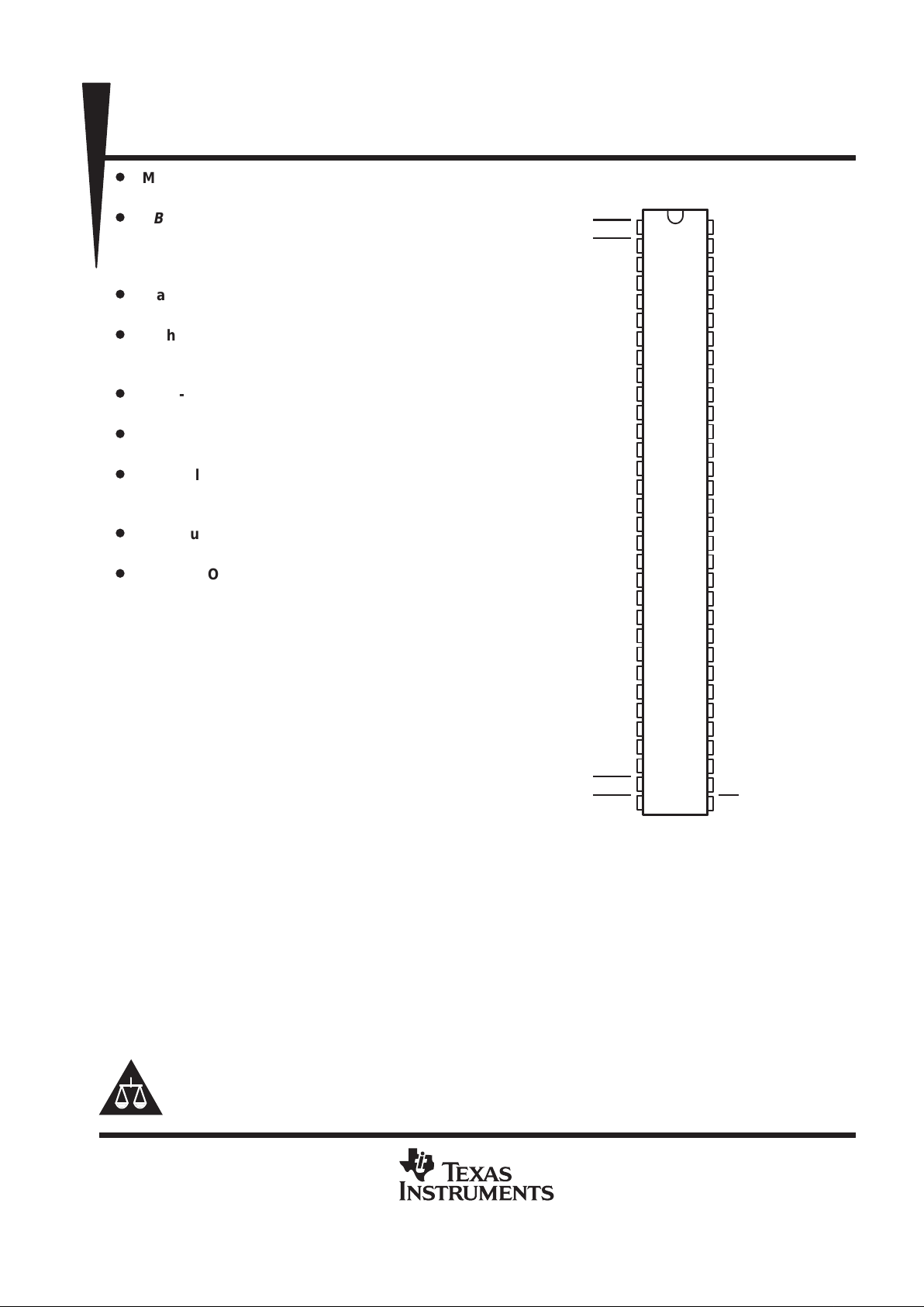
SN74GTL1655 . . . DGG PACKAGE
(TOP VIEW)
1
2
3
4
5
6
7
8
9
10
11
12
13
14
15
16
17
18
19
20
21
22
23
24
25
26
27
28
29
30
31
32
64
63
62
61
60
59
58
57
56
55
54
53
52
51
50
49
48
47
46
45
44
43
42
41
40
39
38
37
36
35
34
33
1OEAB
1OEBA
V
CC
1A1
GND
1A2
1A3
GND
1A4
GND
1A5
GND
1A6
1A7
V
CC
1A8
2A1
GND
2A2
2A3
GND
2A4
2A5
GND
2A6
GND
2A7
V
CC
2A8
GND
2OEAB
2OEBA
CLK
1LEAB
1LEBA
V
ERC
GND
1B1
1B2
GND
1B3
1B4
1B5
GND
1B6
1B7
V
CC
1B8
2B1
GND
2B2
2B3
GND
2B4
2B5
V
REF
2B6
GND
2B7
2B8
BIAS V
CC
2LEAB
2LEBA
OE

SN54GTL1655, SN74GTL1655
16-BIT LVTTL-TO-GTL/GTL+ UNIVERSAL BUS TRANSCEIVERS
WITH LIVE INSERTION
SCBS696E – JULY 1997 – REVISED NOVEMBER 1999
2
POST OFFICE BOX 655303 • DALLAS, TEXAS 75265
description (continued)
The user has the flexibility of using this device at either GTL (VTT = 1.2 V and V
REF
= 0.8 V) or the preferred
higher noise margin GTL+ (VTT = 1.5 V and V
REF
= 1 V) signal levels. GTL+ is the T exas Instruments derivative
of the Gunning transceiver logic (GTL) JEDEC standard JESD 8-3. The B port normally operates at GTL or
GTL+ signal levels, while the A-port and control inputs are compatible with L VTTL logic levels but are not 5-V
tolerant. V
REF
is the reference input voltage for the B port.
These devices are uniquely partitioned as two 8-bit transceivers with individual latch timing and output signals,
but with a common clock and output enable inputs for both transceiver words.
Data flow for each word is determined by the respective latch enables (xLEAB and xLEBA), output enables
(xOEAB and xOEBA), and clock (CLK). The output enables (1OEAB, 1OEBA, 2OEAB, and 2OEBA) control
byte 1 and byte 2 data for the A-to-B and B-to-A directions, respectively.
For A-to-B data flow, the devices operate in the transparent mode when LEAB is high. When LEAB transitions
low, the A data is latched independent of CLK high or low. If LEAB is low, the A data is registered on the CLK
low-to-high transition. When OEAB is low, the outputs are active. With OEAB high, the outputs are in the
high-impedance state.
Data flow for the B-to-A direction is identical, but uses OEBA, LEBA, and CLK. Note that CLK is common to both
directions and both 8-bit words. OE is also common and is used to disable all I/O ports simultaneously.
The ’GTL1655 is featured with adjustable edge-rate control (V
ERC
). Changing V
ERC
input voltage between GND
and VCC adjusts the B-port output rise and fall times. This allows the designer to optimize for various loading
conditions.
These devices are fully specified for live-insertion applications using I
off
, power-up 3-state, and BIAS VCC. The
I
off
circuitry disables the outputs, preventing damaging current backflow through the device when it is powered
down. The power-up 3-state circuitry places the outputs in the high-impedance state during power up and power
down, which prevents driver conflict. The BIAS V
CC
circuitry precharges and preconditions the B-port
input/output connections, preventing disturbance of active data on the backplane during card insertion or
removal, and permits true live-insertion capability.
When V
CC
is between 0 and 1.5 V , the device is in the high-impedance state during power up or power down.
However, to ensure the high-impedance state above 1.5 V, OE should be tied to VCC through a pullup resistor;
the minimum value of the resistor is determined by the current-sinking capability of the driver.
Active bus-hold circuitry holds unused or undriven L VTTL inputs at a valid logic state. Use of pullup or pulldown
resistors with the bus-hold circuitry is not recommended.
The SN54GTL1655 is characterized for operation over the full military temperature range of –55°C to 125°C.
The SN74GTL1655 is characterized for operation from –40°C to 85°C.
SN54GTL1655, SN74GTL1655
16-BIT LVTTL-TO-GTL/GTL+ UNIVERSAL BUS TRANSCEIVERS
WITH LIVE INSERTION
SCBS696E – JULY 1997 – REVISED NOVEMBER 1999
3
POST OFFICE BOX 655303 • DALLAS, TEXAS 75265
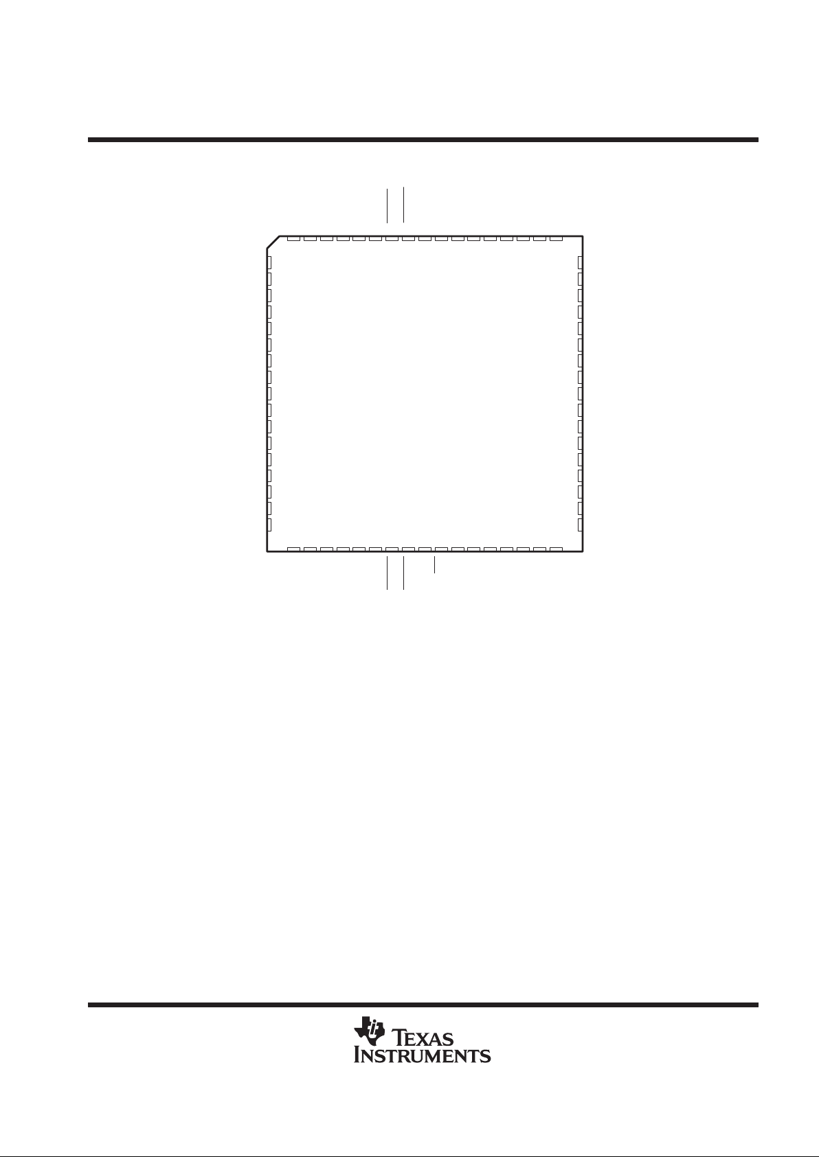
SN54GTL1655 . . . HV PACKAGE
(TOP VIEW)
GND
1A2
1A1
NC
GND
1B1
27 28 29 30 31 32 33 34 35 36 37 38 39 40 41 42 43
9876543216867666564636261
GND
2A7
2A8
GND
2OEAB
OE
2B8
2B7
GND
1OEAB
CLK
1LEAB
1LEBA
1OEBA
1B2
GND
2A6
NC
2OEBA
2LEBA
2LEAB
1A3
2B6
V
ERC
V
CC
GND
NC – No internal connection
CC
V
CC
BIAS V
10
11
12
13
14
15
16
17
18
19
20
21
22
23
24
25
26
60
59
58
57
56
55
54
53
52
51
50
49
48
47
46
45
44
1A4
GND
1A5
GND
1A6
1A7
V
CC
1A8
NC
2A1
GND
2A2
2A3
GND
2A4
2A5
GND
1B3
1B4
1B5
GND
1B6
1B7
V
CC
1B8
NC
2B1
GND
2B2
2B3
GND
2B4
2B5
V
REF
SN54GTL1655, SN74GTL1655
16-BIT LVTTL-TO-GTL/GTL+ UNIVERSAL BUS TRANSCEIVERS
WITH LIVE INSERTION
SCBS696E – JULY 1997 – REVISED NOVEMBER 1999
4
POST OFFICE BOX 655303 • DALLAS, TEXAS 75265
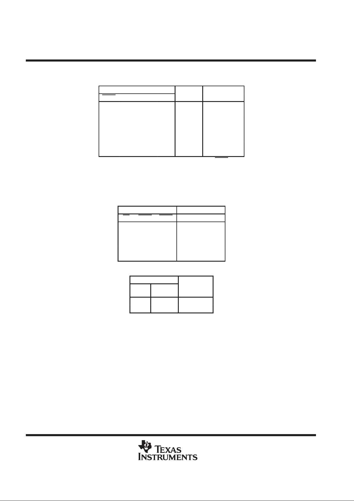
Function Tables
FUNCTION
†
INPUTS
OUTPUT
OEAB LEAB CLK A
B
MODE
H X X X Z Isolation
L HXL L Transparent
L HXH H Transparent
L L ↑ LL Registered
L L ↑ HH Registered
L LHXB
0
‡
Previous State
L L L X B
0
§
Previous State
†
A-to-B data flow is shown. B-to-A flow is similar, but uses OEBA, LEBA,
and CLK.
‡
Output level before the indicated steady-state input conditions were
established, provided that CLK was high before LEAB went low
§
Output level before the indicated steady-state input conditions were
established
OUTPUT ENABLE
INPUTS
OUTPUTS
OE OEAB OEBA A PORT B PORT
L L L Active Active
L LH ZActive
L H L Active Z
L HH Z Z
H X X Z Z
B-PORT EDGE-RATE CONTROL (V
ERC
)
INPUT V
ERC
OUTPUT
LOGIC
LEVEL
NOMINAL
VOLTAGE
B PORT
EDGE RATE
H V
CC
Slow
L GND Fast
SN54GTL1655, SN74GTL1655
16-BIT LVTTL-TO-GTL/GTL+ UNIVERSAL BUS TRANSCEIVERS
WITH LIVE INSERTION
SCBS696E – JULY 1997 – REVISED NOVEMBER 1999
5
POST OFFICE BOX 655303 • DALLAS, TEXAS 75265
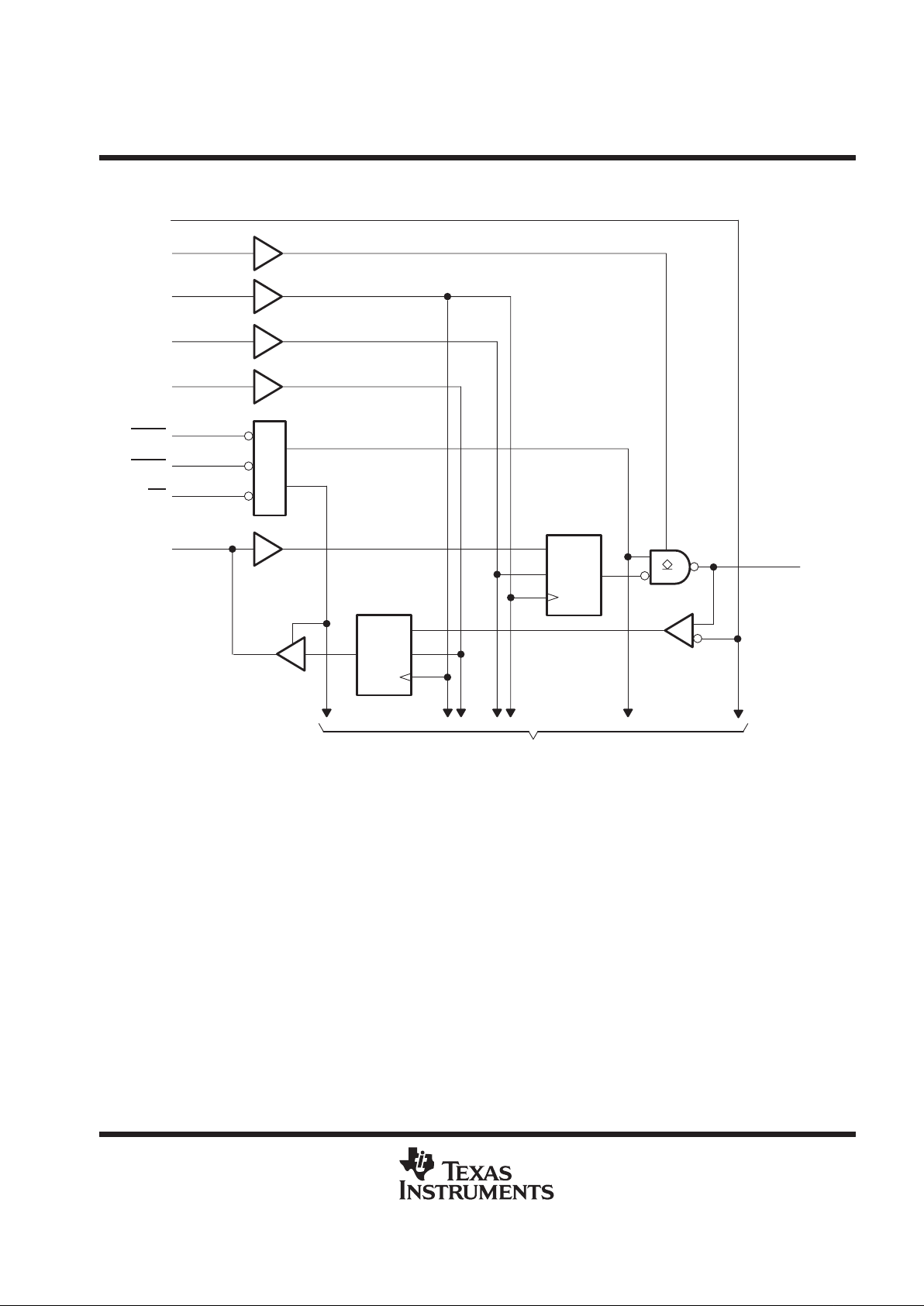
logic diagram (positive logic)
1D
C1
CLK
1D
C1
CLK
1B1
1OEAB
CLK
1LEAB
1LEBA
1OEBA
1A1
1
64
63
62
2
4
59
To Seven Other Channels
OE
33
Pin numbers shown are for the DGG package.
V
ERC
61
V
REF
41

SN54GTL1655, SN74GTL1655
16-BIT LVTTL-TO-GTL/GTL+ UNIVERSAL BUS TRANSCEIVERS
WITH LIVE INSERTION
SCBS696E – JULY 1997 – REVISED NOVEMBER 1999
6
POST OFFICE BOX 655303 • DALLAS, TEXAS 75265
logic diagram (positive logic) (continued)
1D
C1
CLK
1D
C1
CLK
2B1
2OEAB
CLK
2LEAB
2LEBA
2OEBA
2A1
31
64
35
34
32
17
48
To Seven Other Channels
OE
33
Pin numbers shown are for the DGG package.
V
ERC
61
V
REF
41

SN54GTL1655, SN74GTL1655
16-BIT LVTTL-TO-GTL/GTL+ UNIVERSAL BUS TRANSCEIVERS
WITH LIVE INSERTION
SCBS696E – JULY 1997 – REVISED NOVEMBER 1999
7
POST OFFICE BOX 655303 • DALLAS, TEXAS 75265
absolute maximum ratings over operating free-air temperature range (unless otherwise noted)
†
Supply voltage range, VCC, BIAS VCC –0.5 V to 4.6 V. . . . . . . . . . . . . . . . . . . . . . . . . . . . . . . . . . . . . . . . . . . . . . .
Input voltage range, VI (see Note 1): A-port and control pins –0.5 V to 4.6 V. . . . . . . . . . . . . . . . . . . . . . . . . . . .
B port, V
ERC
, and V
REF
–0.5 V to 4.6 V. . . . . . . . . . . . . . . . . . . . . . . . . .
Voltage range applied to any output in the high or power-off state, V
O
(see Note 1): A port –0.5 V to 4.6 V. . . . . . . . . . . . . . . . . . . . . . . . . . . . . . . . . . . . . . . . . . . . . . . . . . . . . . . . . . . .
B port –0.5 V to 4.6 V. . . . . . . . . . . . . . . . . . . . . . . . . . . . . . . . . . . . . . . . . . . . . . . . . . . . . . . . . . . .
Current into any output in the low state, IO: A port 48 mA. . . . . . . . . . . . . . . . . . . . . . . . . . . . . . . . . . . . . . . . . . .
B port 200 mA. . . . . . . . . . . . . . . . . . . . . . . . . . . . . . . . . . . . . . . . . .
Current into any A-port output in the high state, I
O
(see Note 2) 48 mA. . . . . . . . . . . . . . . . . . . . . . . . . . . . . . . .
Continuous current through each VCC or GND ±100 mA. . . . . . . . . . . . . . . . . . . . . . . . . . . . . . . . . . . . . . . . . . . . .
Input clamp current, I
IK
(V
I
< 0) –50 mA. . . . . . . . . . . . . . . . . . . . . . . . . . . . . . . . . . . . . . . . . . . . . . . . . . . . . . . . . . .
Output clamp current, I
OK
(V
O
< 0) –50 mA. . . . . . . . . . . . . . . . . . . . . . . . . . . . . . . . . . . . . . . . . . . . . . . . . . . . . . . .
Package thermal impedance, θJA (see Note 3) 55°C/W. . . . . . . . . . . . . . . . . . . . . . . . . . . . . . . . . . . . . . . . . . . . .
Storage temperature range, T
stg
–65°C to 150°C. . . . . . . . . . . . . . . . . . . . . . . . . . . . . . . . . . . . . . . . . . . . . . . . . . .
†
Stresses beyond those listed under “absolute maximum ratings” may cause permanent damage to the device. These are stress ratings only, and
functional operation of the device at these or any other conditions beyond those indicated under “recommended operating conditions” is not
implied. Exposure to absolute-maximum-rated conditions for extended periods may affect device reliability.
NOTES: 1. The input and output negative-voltage ratings may be exceeded if the input and output clamp-current ratings are observed.
2. This current flows only when the output is in the high state and VO > VCC.
3. The package thermal impedance is calculated in accordance with JESD 51.

SN54GTL1655, SN74GTL1655
16-BIT LVTTL-TO-GTL/GTL+ UNIVERSAL BUS TRANSCEIVERS
WITH LIVE INSERTION
SCBS696E – JULY 1997 – REVISED NOVEMBER 1999
8
POST OFFICE BOX 655303 • DALLAS, TEXAS 75265
recommended operating conditions (see Notes 4 through 6)
SN54GTL1655 SN74GTL1655
MIN NOM MAX MIN NOM MAX
UNIT
BIAS V
CC
Supply voltage 3 3.3 3.6 3 3.3 3.6 V
Termination
GTL 1.14 1.2 1.26 1.14 1.2 1.26
V
TT
voltage
GTL+
1.35 1.5 1.65 1.35 1.5 1.65
V
pp
GTL 0.74 0.8 0.87 0.74 0.8 0.87
V
REF
Suppl
y v
oltage
GTL+ 0.87 1 1.1 0.87 1 1.1
V
p
B port 0 V
TT
0 V
TT
VIInput voltage
Except B port 0 V
CC
0 V
CC
V
B port V
REF
+50 mV V
REF
+50 mV
High-level
V
ERC
V
CC–0.6
V
CC
V
CC–0.6
V
CC
V
IH
input voltage
Except B port
and ERC
2 2
V
B port V
REF
–50 mV V
REF
–50 mV
Low-level
V
ERC
GND 0.6 GND 0.6
V
IL
input voltage
Except B port
and ERC
0.8 0.8
V
I
IK
Input clamp current –18 –18 mA
I
OH
High-level
output current
A port –24 mA
Low-level
A port 24
I
OL
output current
B port
100
mA
∆t/∆V
CC
Power-up ramp rate 200 200 µs/V
T
A
Operating free-air temperature –55 125 –40 85 °C
NOTES: 4. All unused inputs of the device must be held at VCC or GND to ensure proper device operation. Refer to the TI application report,
Implications of Slow or Floating CMOS Inputs
, literature number SCBA004.
5. Normal connection sequence is GND first, BIAS VCC = 3.3 V second, and VCC = 3.3 V , I/O, control inputs, VTT and V
REF
(any order)
last. However, if the B-port I/O precharge is not required, the acceptable connection sequence is GND first and VCC = 3.3 V,
BIAS VCC = 3.3 V , I/O, control inputs, VTT and V
REF
(any order) last. When VCC is connected, the BIAS VCC circuitry is disabled.
6. VTT and RTT can be adjusted to accommodate backplane impedances as long as they do not exceed the DC absolute IOL ratings.
Similarly, V
REF
can be adjusted to optimize noise margins, but normally is 2/3 VTT.
PRODUCT PREVIEW information concerns products in the formative or
design phase of development. Characteristic data and other
specifications are design goals. Texas Instruments reserves the right to
change or discontinue these products without notice.

SN54GTL1655, SN74GTL1655
16-BIT LVTTL-TO-GTL/GTL+ UNIVERSAL BUS TRANSCEIVERS
WITH LIVE INSERTION
SCBS696E – JULY 1997 – REVISED NOVEMBER 1999
9
POST OFFICE BOX 655303 • DALLAS, TEXAS 75265
electrical characteristics over recommended operating free-air temperature range, V
REF
= 1 V and
V
TT
= 1.5 V (unless otherwise noted)
SN54GTL1655 SN74GTL1655
PARAMETER
TEST CONDITIONS
MIN TYP†MAX MIN TYP†MAX
UNIT
V
IK
VCC = 3 V, II = –18 mA –1.2 –1.2 V
VCC = 3 V to 3.6 V, IOH = –100 µA VCC–0.2 VCC–0.2
V
OH
A port
IOH = –12 mA 2.4 2.4
V
V
CC
= 3
V
IOH = –24 mA 2.2 2.2
VCC = 3 V to 3.6 V, IOL = 100 µA 0.2 0.2
A port
IOL = 12 mA 0.4 0.4
V
CC
=
3 V
IOL = 24 mA 0.55 0.55
V
OL
IOL = 40 mA 0.2 0.2
V
B port VCC = 3 V
IOL = 80 mA 0.4 0.4
IOL = 100 mA 0.5 0.5
Control inputs
VI = VCC or GND ±10 ±10
I
I
B port
V
CC
= 3.6
V
VI = VTT or GND ±10 ±10
µ
A
I
off
VCC = 0, VI or VO = 0 to 3.6 V ±100 µA
VI = 0.8 V 75 75
I
I(hold)
A port
V
CC
= 3
V
VI = 2 V –75 –75
µA
()
VCC = 3.6 V‡, VI = 0 to V
CC
±500 ±500
I
OZH
B port VCC = 3.6 V, VO = 1.5 V 10 10 µA
I
OZL
B port VCC = 3.6 V, VO = 0.4 V –10 –10 µA
I
OZ
§
A port VCC = 3.6 V, VO = VCC or GND ±10 ±10 µA
I
OZPU
A port
VCC = 0 to 3.6 V, VO = 0.5 V to 3 V,
OE
= low
±50* ±50 µA
I
OZPD
A port
VCC = 3.6 V to 0, VO = 0.5 V to 3 V,
OE
= low
±50* ±50 µA
=
Outputs high 80 80
I
CC
A or B port
V
CC
= 3.6 V,
IO = 0,
Outputs low 80 80
mA
VI = VCC or GND
Outputs disabled 80 80
∆I
CC
¶
Except B port
VCC = 3.6 V,
A-port or control inputs at VCC or GND,
One input at VCC – 0.6 V
1 1 mA
C
i
Control inputs VI = VCC or 0 3 5 3 5 pF
A port
5 6 5 6
p
C
io
B port
V
O
=
V
CC
or 0
6 8 6 8
pF
* On products compliant to MIL-PRF-38535, this parameter is not production tested.
†
All typical values are at VCC = 3.3 V, TA = 25°C.
‡
This is the bus-hold maximum dynamic current. It is the minimum overdrive current required to switch the input from one state to another.
§
For I/O ports, the parameter IOZ includes the input leakage current.
¶
This is the increase in supply current for each input that is at the specified TTL voltage level rather than VCC or GND.
PRODUCT PREVIEW information concerns products in the formative or
design phase of development. Characteristic data and other
specifications are design goals. Texas Instruments reserves the right to
change or discontinue these products without notice.

SN54GTL1655, SN74GTL1655
16-BIT LVTTL-TO-GTL/GTL+ UNIVERSAL BUS TRANSCEIVERS
WITH LIVE INSERTION
SCBS696E – JULY 1997 – REVISED NOVEMBER 1999
10
POST OFFICE BOX 655303 • DALLAS, TEXAS 75265
live-insertion specifications over recommended operating free-air temperature range
SN54GTL1655 SN74GTL1655
PARAMETER
TEST CONDITIONS
MIN MAX MIN MAX
UNIT
VCC = 0 to 3 V
V (B port) = 0 to 1.2 V,
5 5 mA
I
CC
(BIAS VCC)
VCC = 3 V to 3.6 V
() ,
VI (BIAS VCC) = 3 V to 3.6 V
10 10 µA
V
O
B port VCC = 0, VI (BIAS VCC) = 3.3 V 1 1.2 1 1.2 V
VCC = 0, V (B port) = 0.4 V, VI (BIAS VCC) = 3 V to 3.6 V –1 –1
I
O
B port
VCC = 0 to 3.6 V, OE = 3.3 V 100 100
µA
VCC = 0 to 1.5 V, OE = 0 to 3.3 V 100 100
timing requirements over recommended ranges of supply voltage and operating free-air
temperature, V
TT
= 1.2 V, V
REF
= 0.8 V and V
ERC
= VCC or GND for GTL (unless otherwise noted)
SN54GTL1655 SN74GTL1655
MIN MAX MIN MAX
UNIT
f
clock
Clock frequency 160 160 MHz
LE high 3 3
twPulse duration
CLK high or low 3 3
ns
Data before CLK↑ 2.7 2.7
t
su
Setup time
CLK high 2.8 2.8
ns
Data before LE↓
CLK low 2.6 2.6
Data after CLK↑ 0.4 0.4
thHold time
Data after LE↓ CLK high or low 0.9 0.9
ns
PRODUCT PREVIEW information concerns products in the formative or
design phase of development. Characteristic data and other
specifications are design goals. Texas Instruments reserves the right to
change or discontinue these products without notice.

SN54GTL1655, SN74GTL1655
16-BIT LVTTL-TO-GTL/GTL+ UNIVERSAL BUS TRANSCEIVERS
WITH LIVE INSERTION
SCBS696E – JULY 1997 – REVISED NOVEMBER 1999
11
POST OFFICE BOX 655303 • DALLAS, TEXAS 75265
A-to-B switching characteristics over recommended ranges of supply voltage and operating
free-air temperature, V
TT
= 1.2 V, V
REF
= 0.8 V and V
ERC
= VCC or GND for GTL (see Figure 1)
FROM TO
SN54GTL1655 SN74GTL1655
PARAMETER
(INPUT) (OUTPUT)
MIN MAX MIN MAX
UNIT
f
max
160 160 MHz
t
PLH
A
3.1 5.2 3.1 5.2
t
PHL
V
ERC
= V
CC
B
2.6 6.2 2.6 6.2
ns
t
PLH
CLK
3.4 5.5 3.4 5.5
t
PHL
V
ERC
= V
CC
B
2.4 5.8 2.4 5.8
ns
t
PLH
LEAB
3.5 5.8 3.5 5.8
t
PHL
V
ERC
= V
CC
B
2.6 6.4 2.6 6.4
ns
t
en
OEAB or OE
3.3 5.4 3.3 5.4
t
dis
OEAB or OE
V
ERC
= V
CC
B
2.7 5.9 2.7 5.9
ns
t
PLH
A
2.3 4.3 2.3 4.3
t
PHL
V
ERC
= GND
B
1.9 4.3 1.9 4.3
ns
t
PLH
CLK
2.7 4.8 2.7 4.8
t
PHL
V
ERC
= GND
B
1.8 4.3 1.8 4.3
ns
t
PLH
LEAB
2.8 4.9 2.8 4.9
t
PHL
V
ERC
= GND
B
2 4.8 2 4.8
ns
t
en
OEAB or OE
2.5 4.5 2.5 4.5
t
dis
OEAB or OE
V
ERC
= GND
B
2 4.2 2 4.2
ns
Slew rate (V
ERC
= VCC) Both transitions, B outputs (0.6 V to 1.3 V) 1 1 ns/V
Slew rate (V
ERC
= GND) Both transitions, B outputs (0.6 V to 1.3 V) 1 1 ns/V
t
sk(o)
†
Skew between drivers in the same package
(switching in the same direction)
1 1 ns
t
sk(o)
‡
Skew between drivers
switching in any direction in the same package
1 1 ns
†
Skew values are applicable for through mode only.
‡
Skew values are applicable for CLK mode only, with all outputs switching simultaneously.
PRODUCT PREVIEW information concerns products in the formative or
design phase of development. Characteristic data and other
specifications are design goals. Texas Instruments reserves the right to
change or discontinue these products without notice.

SN54GTL1655, SN74GTL1655
16-BIT LVTTL-TO-GTL/GTL+ UNIVERSAL BUS TRANSCEIVERS
WITH LIVE INSERTION
SCBS696E – JULY 1997 – REVISED NOVEMBER 1999
12
POST OFFICE BOX 655303 • DALLAS, TEXAS 75265
B-to-A switching characteristics over recommended ranges of supply voltage and operating
free-air temperature, V
TT
= 1.2 V and V
REF
= 0.8 V for GTL (see Figure 1)
FROM TO
SN54GTL1655 SN74GTL1655
PARAMETER
(INPUT) (OUTPUT)
MIN MAX MIN MAX
UNIT
f
max
160 160 MHz
t
PLH
1.8 4.7 1.8 4.7
t
PHL
B
A
2.3 4.6 2.3 4.6
ns
t
PLH
1.6 4 1.6 4
t
PHL
CLK
A
1.5 3.4 1.5 3.4
ns
t
PLH
1.7 4 1.7 4
t
PHL
LEBA
A
1.4 3.5 1.4 3.5
ns
t
en
1.3 4.2 1.3 4.2
t
dis
OEBA
or
OE
A
2 6.1 2 6.1
ns
t
sk(o)
†
Skew between drivers in the same package
(switching in the same direction)
1 1 ns
t
sk(o)
‡
Skew between drivers
switching in any direction in the same package
1 1 ns
†
Skew values are applicable for through mode only.
‡
Skew values are applicable for CLK mode only, with all outputs switching simultaneously.
PRODUCT PREVIEW information concerns products in the formative or
design phase of development. Characteristic data and other
specifications are design goals. Texas Instruments reserves the right to
change or discontinue these products without notice.

SN54GTL1655, SN74GTL1655
16-BIT LVTTL-TO-GTL/GTL+ UNIVERSAL BUS TRANSCEIVERS
WITH LIVE INSERTION
SCBS696E – JULY 1997 – REVISED NOVEMBER 1999
13
POST OFFICE BOX 655303 • DALLAS, TEXAS 75265
timing requirements over recommended ranges of supply voltage and operating free-air
temperature, V
TT
= 1.5 V, V
REF
= 1 V and V
ERC
= VCC or GND for GTL+ (unless otherwise noted)
SN54GTL1655 SN74GTL1655
MIN MAX MIN MAX
UNIT
f
clock
Clock frequency 160 160 MHz
LE high 3 3
twPulse duration
CLK high or low 3 3
ns
Data before CLK↑ 2.7 2.7
t
su
Setup time
CLK high 2.8 2.8
ns
Data before LE↓
CLK low 2.6 2.6
Data after CLK↑ 0.4 0.4
thHold time
Data after LE↓ CLK high or low 0.9 0.9
ns
A-to-B switching characteristics over recommended ranges of supply voltage and operating
free-air temperature, V
TT
= 1.5 V, V
REF
= 1 V and V
ERC
= VCC or GND for GTL+ (see Figure 1)
FROM TO
SN54GTL1655 SN74GTL1655
PARAMETER
(INPUT) (OUTPUT)
MIN MAX MIN MAX
UNIT
f
max
160 160 MHz
t
PLH
A
3 5.1 3 5.1
t
PHL
V
ERC
= V
CC
B
2.9 6.5 2.9 6.5
ns
t
PLH
CLK
3.4 5.4 3.4 5.4
t
PHL
V
ERC
= V
CC
B
2.7 6.2 2.7 6.2
ns
t
PLH
LEAB
3.5 5.7 3.5 5.7
t
PHL
V
ERC
= V
CC
B
2.8 6.7 2.8 6.7
ns
t
en
OEAB
3.3 5.4 3.3 5.4
t
dis
OEAB
V
ERC
= V
CC
B
3 6.3 3 6.3
ns
t
en
OE
3 5.5 3 5.5
t
dis
OE
V
ERC
= V
CC
B
3.6 5.8 3.6 5.8
ns
t
PLH
A
2.3 4.3 2.3 4.3
t
PHL
V
ERC
= GND
B
2 4.4 2 4.4
ns
t
PLH
CLK
2.7 4.8 2.7 4.8
t
PHL
V
ERC
= GND
B
1.9 4.5 1.9 4.5
ns
t
PLH
LEAB
2.8 4.9 2.8 4.9
t
PHL
V
ERC
= GND
B
2.1 4.9 2.1 4.9
ns
t
en
OEAB
2.5 4.5 2.5 4.5
t
dis
OEAB
V
ERC
= GND
B
2.1 4.4 2.1 4.4
ns
t
en
OE
2.5 4.6 2.5 4.6
t
dis
OE
V
ERC
= GND
B
2.9 4.9 2.9 4.9
ns
Slew rate (V
ERC
= VCC) Both transitions, B outputs (0.6 V to 1.3 V) 1 1 ns/V
Slew rate (V
ERC
= GND) Both transitions, B outputs (0.6 V to 1.3 V) 1 1 ns/V
t
sk(o)
†
Skew between drivers in the same package
(switching in the same direction)
1 1 ns
t
sk(o)
‡
Skew between drivers
switching in any direction in the same package
1 1 ns
†
Skew values are applicable for through mode only.
‡
Skew values are applicable for CLK mode only, with all outputs switching simultaneously.
PRODUCT PREVIEW information concerns products in the formative or
design phase of development. Characteristic data and other
specifications are design goals. Texas Instruments reserves the right to
change or discontinue these products without notice.

SN54GTL1655, SN74GTL1655
16-BIT LVTTL-TO-GTL/GTL+ UNIVERSAL BUS TRANSCEIVERS
WITH LIVE INSERTION
SCBS696E – JULY 1997 – REVISED NOVEMBER 1999
14
POST OFFICE BOX 655303 • DALLAS, TEXAS 75265
B-to-A switching characteristics over recommended ranges of supply voltage and operating
free-air temperature, V
TT
= 1.5 V and V
REF
= 1 V for GTL+ (see Figure 1)
FROM TO
SN54GTL1655 SN74GTL1655
PARAMETER
(INPUT) (OUTPUT)
MIN MAX MIN MAX
UNIT
f
max
160 160 MHz
t
PLH
2 4.8 2 4.8
t
PHL
B
A
2.4 4.7 2.4 4.7
ns
t
PLH
1.6 4.4 1.6 4.4
t
PHL
CLK
A
1.5 3.4 1.5 3.4
ns
t
PLH
1.7 4 1.7 4
t
PHL
LEBA
A
1.4 3.5 1.4 3.5
ns
t
en
1.3 4.2 1.3 4.2
t
dis
OEBA
A
2 6.1 2 6.1
ns
t
en
2.2 4.7 2.2 4.7
t
dis
OE
A
4.1 6.3 4.1 6.3
ns
t
sk(o)
†
Skew between drivers in the same package
(switching in the same direction)
1 1 ns
t
sk(o)
‡
Skew between drivers
switching in any direction in the same package
1 1 ns
†
Skew values are applicable for through mode only.
‡
Skew values are applicable for CLK mode only, with all outputs switching simultaneously.
PRODUCT PREVIEW information concerns products in the formative or
design phase of development. Characteristic data and other
specifications are design goals. Texas Instruments reserves the right to
change or discontinue these products without notice.

SN54GTL1655, SN74GTL1655
16-BIT LVTTL-TO-GTL/GTL+ UNIVERSAL BUS TRANSCEIVERS
WITH LIVE INSERTION
SCBS696E – JULY 1997 – REVISED NOVEMBER 1999
15
POST OFFICE BOX 655303 • DALLAS, TEXAS 75265
PARAMETER MEASUREMENT INFORMATION
t
h
t
su
From Output
Under Test
CL = 50 pF
(see Note A)
LOAD CIRCUIT FOR A OUTPUTS
S1
6 V
Open
GND
500 Ω
500 Ω
TEST
t
PLH/tPHL
t
PLZ/tPZL
t
PHZ/tPZH
S1
Open
6 V
GND
t
PLH
t
PHL
Output
Control
Output
Waveform 1
S1 at 6 V
(see Note B)
Output
Waveform 2
S1 at GND
(see Note B)
V
OL
V
OH
t
PZL
t
PZH
t
PLZ
t
PHZ
3 V
0 V
V
REF
V
REF
V
TT
V
OL
0 V
VOL + 0.3 V
VOH – 0.3 V
≈0 V
3 V
0 V
0 V
3 V
0 V
t
w
Input
3 V
3 V
3 V
VOLTAGE WAVEFORMS
SETUP AND HOLD TIMES
VOLTAGE WAVEFORMS
PROPAGATION DELAY TIMES
(CLK to B port)
VOLTAGE WAVEFORMS
PULSE DURATION
VOLTAGE WAVEFORMS
ENABLE AND DISABLE TIMES
(A port)
Timing
Input
Data Input
A Port
Output
Input
V
TT
Test
Point
CL = 30 pF
(see Note A)
From Output
Under Test
12.5 Ω
LOAD CIRCUIT FOR B OUTPUTS
t
PLH
t
PHL
0 V
V
OH
V
OL
Input
VOLTAGE WAVEFORMS
PROPAGATION DELAY TIMES
(CLK to A port)
Output
V
REF
V
REF
0 V
V
TT
Data Input
B Port
NOTES: A. CL includes probe and jig capacitance.
B. Waveform 1 is for an output with internal conditions such that the output is low except when disabled by the output control.
Waveform 2 is for an output with internal conditions such that the output is high except when disabled by the output control.
C. All input pulses are supplied by generators having the following characteristics: PRR ≤ 10 MHz, ZO = 50 Ω, tr ≤ 2.5 ns, tf≤ 2.5 ns.
D. The outputs are measured one at a time with one transition per measurement.
E. t
PLZ
and t
PHZ
are the same as t
dis
.
F. t
PZL
and t
PZH
are the same as ten.
1.5 V
1.5 V
1.5 V 1.5 V
1.5 V 1.5 V
1.5 V
1.5 V
1.5 V
1.5 V 1.5 V
1.5 V
1.5 V
1.5 V 1.5 V
3 V
Figure 1. Load Circuits and Voltage Waveforms

IMPORTANT NOTICE
T exas Instruments and its subsidiaries (TI) reserve the right to make changes to their products or to discontinue
any product or service without notice, and advise customers to obtain the latest version of relevant information
to verify, before placing orders, that information being relied on is current and complete. All products are sold
subject to the terms and conditions of sale supplied at the time of order acknowledgement, including those
pertaining to warranty, patent infringement, and limitation of liability.
TI warrants performance of its semiconductor products to the specifications applicable at the time of sale in
accordance with TI’s standard warranty. Testing and other quality control techniques are utilized to the extent
TI deems necessary to support this warranty. Specific testing of all parameters of each device is not necessarily
performed, except those mandated by government requirements.
CERT AIN APPLICATIONS USING SEMICONDUCTOR PRODUCTS MAY INVOLVE POTENTIAL RISKS OF
DEATH, PERSONAL INJURY, OR SEVERE PROPERTY OR ENVIRONMENTAL DAMAGE (“CRITICAL
APPLICATIONS”). TI SEMICONDUCTOR PRODUCTS ARE NOT DESIGNED, AUTHORIZED, OR
WARRANTED TO BE SUITABLE FOR USE IN LIFE-SUPPORT DEVICES OR SYSTEMS OR OTHER
CRITICAL APPLICATIONS. INCLUSION OF TI PRODUCTS IN SUCH APPLICA TIONS IS UNDERSTOOD T O
BE FULLY AT THE CUSTOMER’S RISK.
In order to minimize risks associated with the customer’s applications, adequate design and operating
safeguards must be provided by the customer to minimize inherent or procedural hazards.
TI assumes no liability for applications assistance or customer product design. TI does not warrant or represent
that any license, either express or implied, is granted under any patent right, copyright, mask work right, or other
intellectual property right of TI covering or relating to any combination, machine, or process in which such
semiconductor products or services might be or are used. TI’s publication of information regarding any third
party’s products or services does not constitute TI’s approval, warranty or endorsement thereof.
Copyright 1999, Texas Instruments Incorporated
 Loading...