

D
Compatible With IEEE Std 1 194.1-1991
(BTL)
D
TTL A Port, Backplane Transceiver Logic
(BTL) B
D
Open-Collector B-Port Outputs Sink
Port
100 mA
D
BIAS VCC Pin Minimizes Signal Distortion
During Live Insertion/Withdrawal
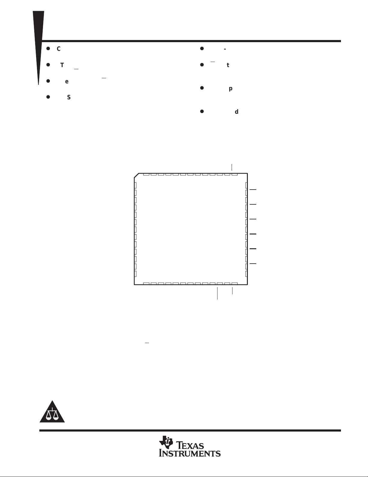
8-BIT TTL/BTL REGISTERED TRANSCEIVER
D
D
D
D
RC PACKAGE
(TOP VIEW)
SN74FB2033K
SCBS472E – MAY 1994 – REVISED JUNE 1997
High-Impedance State During Power Up
and Power Down
B-Port Biasing Network Preconditions the
Connector and PC Trace to the BTL
High-Level Voltage
TTL-Input Structures Incorporate Active
Clamping Networks to Aid in Line
Termination
Packaged in Plastic Quad Flatpack
description
GND
AO2
AI3
AO3
AI4
AO4
LOOPBACK
AI5
AO5
AI6
AO6
AI7
GND
CC
CC
AO1
AI8
AI1
AO8
GND
V
V
GND
CC
CLKAB/LEAB
IMODE1
IMODE0
BG V
CC
V
OMODE0
OMODE1
CLKBA/LEBA
OEA
OEB
AI2
52 51 50 49 48 47 46 45 44 43 42 41 40
1
2
3
4
5
6
7
8
9
10
11
12
13
14 15 16 17 18 19 20 21 22 23 24 25 26
AO7
CC
BIAS V
BG GND
B1
39
38
37
36
35
34
33
32
31
30
29
28
27
B8
OEB
GND
GND
B2
GND
B3
GND
B4
GND
B5
GND
B6
GND
B7
GND
The SN74FB2033K is an 8-bit transceiver featuring a split input (AI) and output (AO) bus on the TTL-level A port.
The common I/O, open-collector B port operates at backplane transceiver logic (BTL) signal levels. The
SN74FB2033K is specifically designed to be compatible with IEEE Std 1194.1-1991.
The logic element for data flow in each direction is configured by two mode inputs (IMODE1 and IMODE0 for
B-to-A, OMODE1 and OMODE0 for A-to-B) as a buffer , a D-type flip-flop, or a D-type latch. When configured
in the buffer mode, the inverted input data appears at the output port. In the flip-flop mode, data is stored on
the rising edge of the appropriate clock input (CLKAB/LEAB or CLKBA/LEBA). In the latch mode, the clock
inputs serve as active-high transparent latch enables.
Please be aware that an important notice concerning availability, standard warranty, and use in critical applications of
Texas Instruments semiconductor products and disclaimers thereto appears at the end of this data sheet.
PRODUCTION DATA information is current as of publication date.
Products conform to specifications per the terms of Texas Instruments
standard warranty. Production processing does not necessarily include
testing of all parameters.
POST OFFICE BOX 655303 • DALLAS, TEXAS 75265
Copyright 1997, Texas Instruments Incorporated
1
SN74FB2033K
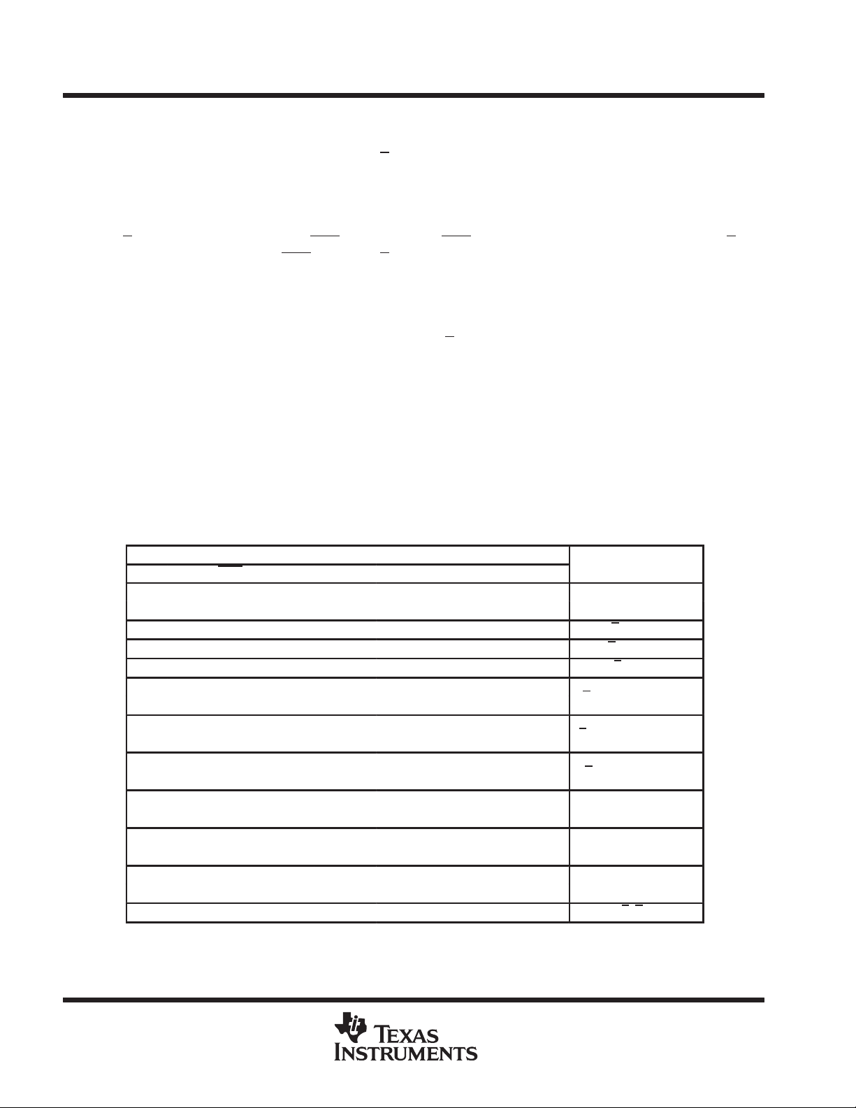
FUNCTION/MODE
Isolation
B
B
flip-fl
B
AI to AO, buffer mode
AI to AO, flip-flop mode
AI to AO, latch mode
8-BIT TTL/BTL REGISTERED TRANSCEIVER
SCBS472E – MAY 1994 – REVISED JUNE 1997
description (continued)
Data flow in the B-to-A direction, regardless of the logic element selected, is further controlled by the
LOOPBACK input. When LOOPBACK is low, B-port data is the B-to-A input. When LOOPBACK is high, the
output of the selected A-to-B logic element (before inversion) is the B-to-A input.
The AO port-enable/-disable control is provided by OEA. When OEA is low or when V
is less than 2.5 V , the
CC
AO port is in the high-impedance state. When OEA is high, the AO port is active (high or low logic levels).
port is controlled by OEB and OEB. If OEB is low, or OEB is high, or when VCC is less than 2.5 V , the B port
The B
is inactive. If OEB is high and OEB
BG V
and BG GND are the bias-generator reference inputs.
CC
is low, the B port is active.
The A-to-B and B-to-A logic elements are active, regardless of the state of their associated outputs. The logic
elements can enter new data (in flip-flop and latch modes) or retain previously stored data while the associated
outputs are in the high-impedance (AO port) or inactive (B port) states.
Output clamps are provided on the BTL outputs to reduce switching noise. One clamp reduces inductive ringing
effects on VOH during a low-to-high transition. The other clamps out ringing below the BTL VOL voltage of 0.75 V .
Both of these clamps are active only during ac switching and do not affect the BTL outputs during steady-state
conditions.
BIAS VCC establishes a voltage between 1.62 V and 2.1 V on the BTL outputs when VCC is not connected.
The SN74FB2033K is characterized for operation from 0°C to 70°C.
Function Tables
FUNCTION
INPUTS
OEA OEB OEB OMODE1 OMODE0 IMODE1 IMODE0 LOOPBACK
L L X X X X X X
L XH X X X X X
X H L L L X X X AI to B, buffer mode
X H L L H X X X AI to B, flip-flop mode
X H L H X X X X AI to B, latch mode
H L X X X L L L
H XH X X L L L
H L X X X L H L
H XH X X L H L
H L X X X H X L
H XH X X H X L
H L X X X L L H
H XH X X L L H
H L X X X L H H
H XH X X L H H
H L X X X H X H
H XH X X H X H
H H L X X X X L AI to B, B to AO
to AO, buffer mode
to AO,
to AO, latch mode
op mode
p
p
2
POST OFFICE BOX 655303 • DALLAS, TEXAS 75265
OUTPUT
OUTPUT
SN74FB2033K
8-BIT TTL/BTL REGISTERED TRANSCEIVER
SCBS472E – MAY 1994 – REVISED JUNE 1997
Function Tables (Continued)
ENABLE/DISABLE
INPUTS
OEA OEB OEB AO B
L X X Hi Z
H X X Active
X LL Inactive (H)
X LH Inactive (H)
X HL Active
X H H Inactive (H)
BUFFER
INPUT
L H
H L
LATCH
INPUTS
CLK/LE DATA
H L H
H HL
L X Q
OUTPUTS
OUTPUT
0
LOOPBACK
LOOPBACK
L B port
H Point P
†
Q is the input to the B-to-A
logic element.
‡
P is the output of the A-to-B
logic element (see functional
block diagram).
SELECT
INPUTS
MODE1 MODE0
L L Buffer
L H Flip-flop
H X Latch
INPUTS
CLK/LE DATA
L X Q
↑ LH
↑ H L
SELECTED-LOGIC
ELEMENT
FLIP-FLOP
†
Q
‡
0
POST OFFICE BOX 655303 • DALLAS, TEXAS 75265
3

SN74FB2033K
8-BIT TTL/BTL REGISTERED TRANSCEIVER
SCBS472E – MAY 1994 – REVISED JUNE 1997
functional block diagram
23
OEB
24
OEB
AI1
21
20
47
Transceiver
1D
C1
50
1D
C1
OMODE1
OMODE0
CLKAB/LEAB
40
B1
P
IMODE1
IMODE0
CLKBA/LEBA
AO1
OEA
LOOPBACK
46
45
19
51
43
7
One of Eight Channels
Transceiver
1D
C1
Q
1D
C1
One of Eight Channels
4
POST OFFICE BOX 655303 • DALLAS, TEXAS 75265
 Loading...